ISSN (Online): 2320-9364, ISSN (Print): 2320-9356
www.ijres.org Volume 4 Issue 10 ǁ October. 2016 ǁ PP. 40-48
Design and simulation of multi-sector switchable antenna array
for the frequency range of 2.4 GHz Wi-Fi networks
Yuri Nechaev
1,
Popova N.V.
2, Peshkov I.V.
2 1(Information systems Department/ Voronezh State University, Russia)
2(Radioelectronics and Computer Techniques Department / Elets State University, Russia)
ABSTRACT
:
The paper describes the calculation and simulation of microstrip antenna array. The basic formulas, graphs, directional pattern.Keywords
-
simulation, microstrip antennas, calculation of microstrip antenna array.I.
INTRODUCTION
Currently there is an intensive use of wireless telecommunications networks to transmit information, among which the Wi-Fi network is particularly popular. It is not always possible to achieve a high data transfer speed even in the city due to the low signal strength and a large number of noise sources. It is known that the attenuation of the signals is caused by a lot of obstacles (reinforced concrete structures, trees, etc.) in the path of propagation of electromagnetic radiation, as well as the significant distance between the access point and subscribers.
To overcome this problem, there is intense enhancement of microstrip antennas, featuring a large variety of designs and are suitable for applications as both independent antennas and antenna arrays elements. The working frequency range of microstrip antennas extends from 300 MHz to 20 GHz.
Stripline and microstrip antenna are able to radiate with linear, circular and elliptical polarization, allowing for suitable design solutions to provide two or multi-frequency modes, make it easy to combine many elementary emitters in a phased antenna arrays and place them on the complex shape surface. The big advantage of such antennas are low weight and size, simple structure, high fabrication precision [1].
II.
BLOCK
DIAGRAM
OF
THE
DEVICE
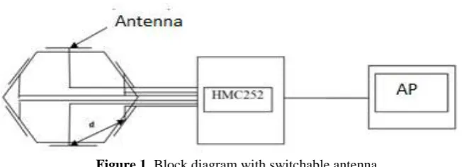
The useful information signal gain and the interference suppression are necessary to develop an antenna array with the coverage of 360°. Each sector should have a maximum gain in a given frequency band (2.4-2.5 GHz). In addition, it is necessary to suppress reception of all signals incident from other directions. Based on the above considerations the configuration of the six switchable spatial sectors is selected.
The most important parameter is the lattice spacing (the distance between the phase centers of emitters) along the respective axes. The array spacing is chosen based on the following factors:
1) Excluding the possibility of emergence of secondary principal maxima of the directional characteristic. That is d<0,9λ0;
2) Elimination of the influence of microstrip antennas at each other in the array, because this leads to changes in the parameters of the emitters, such as, input impedance, resonant frequency, and also worsens the agreement in the working frequency band and the efficiency of the antenna. To eliminate this phenomenon, the distance between the emitters should be selected based on the conditions d>0,5λ0 [2].
Based on these recommendations, the array spacing must lie within 0,5•λ0<d<0,9•λ0. Express this inequality using the unit of length:
60,25 < d < 108,45 mm.
We will take the interelement spacing: d=0,7•λ0=85 mm.
Figure 1. Block diagram with switchable antenna
The each emitter (Antenna) is connected to the RF switch (such as HMC252QS24E), which in turn is connected to an input of the access point (AP). The channel is manually selected with the highest output power.
III.
CALCULATION
OF
THE
MICROSTRIP
ANTENNA
PARAMETERS
FOR
FREQUENCY
2.4
GHZ
Calculation of parameters of microstrip antenna is as follows [3]: The optimum width of a rectangular emitter:
𝑊 = 𝑐
2𝑓0
𝜀𝛾 + 1
2
−0.5
= 3 ∗ 10
8
2 ∗ 2.4 ∗ 109
1 + 1 2
−0.5
= 0.0625 (𝑚), (1)
where f0 - the resonant frequency of the antenna; εγ - dielectric permittivity; с - speed of light.
The environment around the emitter is not homogeneous, as one side of the radiator is a dielectric, and the other is air. Therefore, the effective dielectric constant of the emitter is estimated by the formula:
𝜀𝑒 =
𝜀𝛾+ 1
2 +
𝜀𝛾− 1
2
1 + 12 𝑊
−0.5
=1 + 1
2 +
1 − 1 2
1 + 12 ∗ 0,003 0.0625
−0.5
= 1, (2)
The length of the emitter is equal to:
𝐿 = 𝑐
2𝑓0 𝜀𝑒
− 2𝛥𝑙 = 3 ∗ 10
8
2 ∗ 2,4 ∗ 109 1− 2 ∗ 0,0021 = 0.0584 (𝑚), (3)
where ∆l – changing the length of the boundary fields at the ends of the radiator, εе — effective dielectric permittivity. The value of ∆l can be estimated using the expression:
𝛥𝑙 = 0.412 𝜀𝑒+ 0.3 𝑊
+ 0.264 𝜀𝑒− 0.258 𝑊 + 0.8
= 0.412 ∗ 0,003
1 + 0.3 0.06250,003 + 0.264
1 − 0.258 0.06250,003 + 0.8
= 0.0021 (𝑚), (4)
At the resonant frequency, the input impedance of the radiating antenna screen is defined by the equations:
𝑍𝑖𝑛 =
1 2𝐺1
= 1
2 ∗ 0,002989= 167,2733 (𝑂𝑚), (5)
where
𝐺1=
1 90
𝑊 𝜆0
2
= 1 90
0,0625 0,1205
2
= 0,002989 , (6)
where 𝜆0 - wavelength, 𝜆0= 0,1205 𝑚.
At the resonance the input impedance is purely resistive. A place of power is calculated using the input resistance of the screen. The input impedance varies depending on the location of the feed point y0:
𝑅𝑖𝑛 = 𝑍𝑖𝑛∗ 𝑐𝑜𝑠2
𝜋
𝐿𝑦0 , (7)
Y0 is expressed from this formula:
𝑦0= 𝑎𝑟𝑐𝑐𝑜𝑠
𝑅𝑖𝑛
𝑍𝑖𝑛
∗𝐿
𝜋= 𝑎𝑟𝑐𝑐𝑜𝑠 50 167,2733 ∗
0.0584
𝜋 = 0,01884 (m), (8)
Table 1. Values of the size of the microstrip antenna
Name Value (m)
W 0,0625
L 0,0584
y0 0,01884
∆l 0,0021
h 0,003
εy 1
Now we know the dimensions of the radiating screen. The length and width of the grounding screen are calculated by the following formulas:
𝐿𝑔 = 6 + 𝐿 =6*0,003+0,0584= 0,077 (m) (9)
𝑊𝑔 = 6 + 𝑊=6*0,003+0,0625 = 0,0805 (m) (10)
IV.
SIMULATION
OF
MICROSTRIP
ANTENNA
The creation of a model of the analyzed object is shown in fig. 2.
Figure.2. View from above
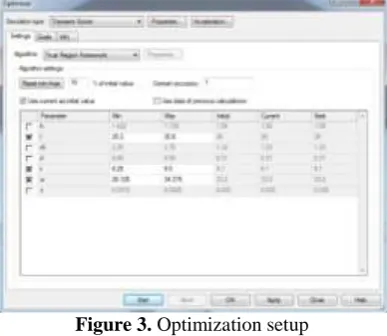
So as to improve the antenna settings in the program there is a function optimization (fig. 3). It automatically selects the size of the antenna to improve the specified characteristics [4].
Figure 3. Optimization setup
After optimization, we obtain the following characteristics shown in table 2.
Table 2. Data of calculations for the antenna after optimization
Name Value Value after optimization
W, (м) 0,0625 0,0605
L, (м) 0,058 0,055
Wg, (м) 0,0805 0,0785
Lg, (м) 0,077 0,073
y0, (м) 0,01884 0,017
∆l, (м) 0,0021 -
h, (м) 0,003 -
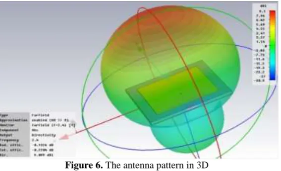
Here are the results of calculation of parameters in the frequency range previously selected (fig. 4-6).
Figure 4. Voltage standing wave ratio
Standing wave ratio (VSWR) characterizes matching of the antenna and feeder. The VSWR is numerically equal to the ratio of the maximum value of the amplitude of the electric or magnetic field of the standing wave in the transmission line to the smallest one. Ideally, the VSWR = 1 [5].
Figure 5. The radiation pattern in the polar coordinate system
Figure 6. The antenna pattern in 3D
V.
MAKING
THE
SINGLE
ANTENNA
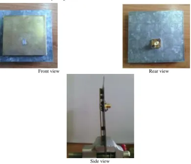
In accordance with the calculations the antenna from a sheet of brass (radiant screen) and galvanized iron (ground screen) (fig. 7) was made. The dielectric between the two screens is the air. The antenna is connected to the Wi-Fi router by using the SMA connector.
Front view Rear view
Side view
Figure 7. Microstrip antenna, made from sheet brass and galvanized iron
VI.
THE
SWITCHING
UNIT
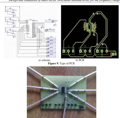
Chip HMC252QS24 is a high-frequency switch operating in the range from 0 to 3 GHz. The control switching is carried out by submitting the codeword TTL levels on the addresses inputs [6].By that way, switching between one input and all the six outputs is carried out of the chip (fig. 8).
Figure 8. Block diagram of the chip HMC252QS24 work.
a) scheme; b) PCB
Figure 9. Type of PCB
Figure 10. The appearance switch designed for microstrip antenna array
When applied to three inputs of different combinations of high and low TTL levels, the chip turns on one of the outputs and transmits the RF signal to the corresponding antennas.
Table 3. The truth table chip HMC252QS24
Control input Signal path state
А В С RFCOM to:
LOW LOW LOW RF1
HIGH LOW LOW RF2
LOW HIGH LOW RF3
HIGH HIGH LOW RF4
LOW LOW HIGH RF5
HIGH LOW HIGH RF6
LOW HIGH HIGH All off
Figure 11. External view of the developed antenna array
VII.
EXPERIMENTAL
VERIFICATION
OF
DEVICE
A Wi-Fi access point was used for testing the antenna array.
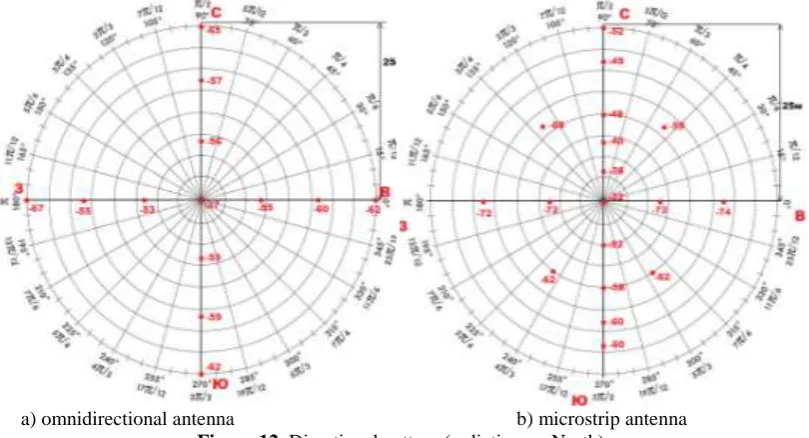
Testing of microstrip antennas was carried out by comparing it with a conventional omnidirectional antenna in conditions close to ideal (the lack of obstacles on the signal propagation). Using a special device the values of the signal strength (dBm) at various points were obtained and the measurement results are drawn in the polar coordinate system (fig. 12).
a) omnidirectional antenna b) microstrip antenna
Figure 12. Directional pattern (radiation on North)
From this radiation pattern it is seen that the whip antenna is the isotropic radiator (radiation occurs in all directions with the same signal strength).
The following measurements were performed for microstrip directional antenna, which has the best characteristics of the radiation that can be seen from fig. 12 (b).
From fig. 12 a), b) it is seen that the designed antenna in the direction of the main lobe has gain up to 15 dBm higher than the standard omnidirectional. In this case, there is a significant increase in throughput of the wireless communication channel. Since the designed microstrip antenna has a higher directivity factor, the signal strength of the received signal is reduced in directions different from the main.
a) omnidirectional antenna b) designed antenna
Figure 13. Data transfer rate
As can be seen from the measurements, the speed of acquiring data using the microstrip antenna exceeds the receive rate using the whip antenna up 13 Mbps, and the transmission speed of 22 Mbps.
To check the antenna PCB with RF-key was connected to Wi-Fi router. The signal is switched to the appropriate output when applying the various code combinations of TTL levels on the address inputs
In the first case, in accordance with the code 110 the signal switched to the output RF4.
Figure 14. Measuring signal strength on the antenna No. 4.
As can be seen from fig. 14, now the radiation is incident on the antenna No. 4. The measured signal power within its radiation pattern is -25 dBm. The signal power on the antennas, which do not correspond to the codeword 110, is substantially below of the power from the No.4 antenna.
VIII.
CONCLUSION
In this paper, we have considered the basic principles of modeling and design of antennas and antenna arrays.
change the antenna parameters and watch the changes in its characteristics (size optimization, VSWR, directivity, traveling-wave ratio, etc.).
Basic calculations were made in the software environment GNU Octave, which allows without rounding and with a small error to make all the necessary calculations.
The structural scheme was developed in the environment of Schematics of a multifunctional development environment electronic devices DipTrace, printed circuit boards – PCB Layout in the same software environment.
The data obtained were prototypes, which, subsequently, were compared to serial samples of antennas, built the radiation pattern and the reading capacity of the investigated antennas.
Based on shot parameters, it was concluded that this type of antennas in many respects superior to the standard antennas used in modern Wi-Fi routers:
signal strength of microstrip antennas is 20% more than signal strength whip antenna;
data transfer rate increased by 17%;
increased the range of radiation.
Summing up the paper we can say that this model can go into production as the standard antenna for Wi-Fi routers High-End [7].
REFERENCES
[1]. Panchenko B.A., Nefedov E.I. Mikropoloskovyye antenny [Microstrip antennas], Moscow, Radio i Svyaz’ Publ., 1986. — 144 p., Ill. — pp. 29-88.
[2]. Edited by Voskresenskiy D.I. Ustroystva SVCH i antenny. Proyektirovaniye fazirovannykh antennykh
reshetok [Microwave devices and antennas. Designing phased antennas arrays], Moscow, Radiotekhnika Publ., 2012. — 744 p.
[3]. Los’ V.F. Mikropoloskovyye i dielektricheskiye rezonatornyye antenny. SAPR-modeli: metody
matematicheskogo modelirovaniya [Microstrip and dielectric resonator antennas. CAD models: methods of mathematical modeling], edited by Bakhrakh L.D. Л.Д., Moscow, IPRZHR Publ., 2002. — 96 p.
[4]. Yurtsev O.A., Bobkov U.U., Kizimenko V.V., Yubko A.P., Gerasimovich G.V. Modelirovaniye antenn
v rezhimakh izlucheniya i rasseyaniya v paketakh CST Studio, HFSS, FEKO i
uzkospetsializirovannykh programmakh [Simulation of antennas and scattering radiation modes in CST Studio packages, HFSS, FEKO and specialized programs], Minsk, BGUIR Publ., 2012. — 62 p.: Ill.
[5]. Kocherzhevskiy G.N., Yerokhin G.A., Kozyrev N.D. Antenno-fidernyye ustroystva: Uchebnik dlya
vuzov [Antenna-feeder devices: A Textbook for high schools], Moscow, Radio i Svyaz’ Publ., 1989. — 352 p.: Ill.
[6]. HMC252QS24 Datasheet (PDF) — Hittite Microwave Corporation [Electronic resource]: Reference
resource. / Hittite Microwave Corporation. –
http://www.alldatasheet.com/datasheet-pdf/pdf/80880/HITTITE/HMC252QS24.html.
[7]. Antenny dlya Wi-Fi ustroystv [Antennas for Wi-Fi devices], [Electronic resource], —