ST
Sitronix
ST7036
Preliminary
Dot Matrix LCD Controller/Driver
Features
z 5 x 8 dot matrix possible z Low power operation support:
-- 2.7 to 5.5V
z Range of LCD driver power
-- 2.7 to 7.0V
z 4-bit, 8-bit, serial or 400kbits/s fast I2C-bus MPU interface enabled
z 80 x 8-bit display RAM (80 characters max.) z 10,240-bit character generator ROM for a
totalof 256 character fonts(max)
z 64 x 8-bit character generator RAM(max) z Support two display mode:
16-com x 100-seg and 80 ICON 24-com x 80-seg and 80 ICON
z 16 x 5 –bit ICON RAM(max)
z Wide range of instruction functions:
Display clear, cursor home, display on/off, cursor on/off, display character blink, cursor shift, display shift, double height font
z Automatic reset circuit that initializes the controller/driver after power on and external reset pin
z Internal oscillator(Frequency=540kHz) and external clock
z Built-in voltage booster and follower circuit (low power consumption )
z COM/SEG direction selectable
z Multi-selectable for CGRAM/CGROM size z Instruction compatible to ST7066U and
KS0066U and HD44780 z Available in COG type
Description
The ST7036 dot-matrix liquid crystal display controller and driver LSI displays alphanumeric, Japanese kana
characters, and symbols. It can be configured to drive a dot-matrix liquid crystal display under the control of a 4-/ 8-bit, serial or fast I2C interface microprocessor. Since all the functions such as display RAM, character generator, and liquid crystal driver, required for driving a dot-matrix liquid crystal display are internally provided on one chip, a minimal system can be interfaced with this
controller/driver.
The ST7036 character generator ROM is extended to generate 256 5x8dot character fonts for a total of 256 different character fonts. The low power supply (2.7V to
5.5V) of the ST7036 is suitable for any portable battery-driven product requiring low power dissipation. The ST7036 LCD driver consists of 17 common signal drivers and 100 segment signal drivers. And the second mode is consists of 25 common signal and 80 segment signal drivers. The maximum display RAM size can be either 80 characters in 1-line display or 40 characters in 2-line display or 16 characters in 3-line. A single ST7036 can display up to one 20-character line or two 20-character lines or three 16-character lines.
No extra drivers can be cascaded.
ST7036
6800-4bit / 8bit (without IIC interface) / 4-wire SPIST7036i
IIC interfaceproduct Name
Character generator
ROM Size
OPR1 OPR2 Support Character
ST7036-0A 256 1 1 English / Japan/Europe
- - -
Note:
I²C option not available for EA DOG series !
ST7036 Serial Specification Revision History
Version Date
Description
0.1a 2003/04/28 1st Edition
0.1b 2003/06/03 PAD Dimension: IC L mark location modified Chip Size X/Y modified 0.2a 2003/09/01 1. Include ST7036i
1.0 2003/10/24 1. Add application circuit for 3 line display. 2. 4 bit interface program example modified. 1.1 2003/12/24 1. Remove the instruction of frequency adjust. 2. Add the detail of CGRAM/CGROM arrangement.
Pad Dimensions
¾
Chip Size: 5190.0X910.0 µm
¾
Bump Pitch : 55 µm ( min )
¾
Bump Height : 17 µm ( typ. )
¾
Bump Size :
z
Pad No.1~52 : 56 x 72 µm
Pad Location Coordinates(N3=0 1 line/2 line)
Pad No. Function
X
Y
Pad No. Function
X
Y
1 XRESET 1859 393 41 CLS -1181 393 2 OSC 1783 393 42 CAP1N -1257 393 3 VDD 1707 393 43 CAP1N -1333 393 4 RS 1631 393 44 VOUT -1409 393 5 CSB 1555 393 45 VOUT -1485 393 6 RW 1479 393 46 V0 -1561 393 7 E 1403 393 47 V0 -1637 393 8 DB0 1327 393 48 V1 -1713 393 9 DB1 1251 393 49 V2 -1789 393 10 DB2 1175 393 50 V3 -1865 393 11 DB3 1099 393 51 V4 -1941 393 12 DB4 1023 393 52 NC -2017 393 13 DB5 947 393 53 COM[8] -2125 378 14 DB6 871 393 54 COM[7] -2180 378 15 DB7 795 393 55 COM[6] -2235 378 16 VSS 719 393 56 COM[5] -2290 378 17 VSS 643 393 57 COM[4] -2518 365 18 VSS 567 393 58 COM[3] -2518 310 19 OPF1 491 393 59 COM[2] -2518 255 20 OPF2 415 393 60 COM[1] -2518 200 21 OPR1 339 393 61 COMI1 -2518 145 22 OPR2 263 393 62 SEG[1] -2518 90 23 SHLC 187 393 63 SEG[2] -2518 35 24 SHLS 111 393 64 SEG[3] -2518 -20 25 N3 35 393 65 SEG[4] -2518 -75 26 TEST1 -41 393 66 SEG[5] -2518 -130 27 VDD -117 393 67 SEG[6] -2518 -185 28 VDD -193 393 68 SEG[7] -2518 -240 29 VDD -269 393 69 SEG[8] -2518 -295 30 VIN -345 393 70 SEG[9] -2518 -350 31 VIN -421 393 71 SEG[10] -2253 -378 32 VOUT -497 393 72 SEG[11] -2198 -378 33 VOUT -573 393 73 SEG[12] -2143 -378 34 PSB -649 393 74 SEG[13] -2088 -378 35 VSS -725 393 75 SEG[14] -2033 -378 36 PSI2B -801 393 76 SEG[15] -1978 -378 37 CAP1P -877 393 77 SEG[16] -1923 -378
Pad No. Function
X
Y
Pad No. Function
X
Y
81 SEG[20] -1703 -378 121 SEG[60] 497 -378 82 SEG[21] -1648 -378 122 SEG[61] 552 -378 83 SEG[22] -1593 -378 123 SEG[62] 607 -378 84 SEG[23] -1538 -378 124 SEG[63] 662 -378 85 SEG[24] -1483 -378 125 SEG[64] 717 -378 86 SEG[25] -1428 -378 126 SEG[65] 772 -378 87 SEG[26] -1373 -378 127 SEG[66] 827 -378 88 SEG[27] -1318 -378 128 SEG[67] 882 -378 89 SEG[28] -1263 -378 129 SEG[68] 937 -378 90 SEG[29] -1208 -378 130 SEG[69] 992 -378 91 SEG[30] -1153 -378 131 SEG[70] 1047 -378 92 SEG[31] -1098 -378 132 SEG[71] 1102 -378 93 SEG[32] -1043 -378 133 SEG[72] 1157 -378 94 SEG[33] -988 -378 134 SEG[73] 1212 -378 95 SEG[34] -933 -378 135 SEG[74] 1267 -378 96 SEG[35] -878 -378 136 SEG[75] 1322 -378 97 SEG[36] -823 -378 137 SEG[76] 1377 -378 98 SEG[37] -768 -378 138 SEG[77] 1432 -378 99 SEG[38] -713 -378 139 SEG[78] 1487 -378 100 SEG[39] -658 -378 140 SEG[79] 1542 -378 101 SEG[40] -603 -378 141 SEG[80] 1597 -378 102 SEG[41] -548 -378 142 SEG[81] 1652 -378 103 SEG[42] -493 -378 143 SEG[82] 1707 -378 104 SEG[43] -438 -378 144 SEG[83] 1762 -378 105 SEG[44] -383 -378 145 SEG[84] 1817 -378 106 SEG[45] -328 -378 146 SEG[85] 1872 -378 107 SEG[46] -273 -378 147 SEG[86] 1927 -378 108 SEG[47] -218 -378 148 SEG[87] 1982 -378 109 SEG[48] -163 -378 149 SEG[88] 2037 -378 110 SEG[49] -108 -378 150 SEG[89] 2092 -378 111 SEG[50] -53 -378 151 SEG[90] 2147 -378 112 SEG[51] 2 -378 152 SEG[91] 2202 -378 113 SEG[52] 57 -378 153 SEG[92] 2518 -350 114 SEG[53] 112 -378 154 SEG[93] 2518 -295 115 SEG[54] 167 -378 155 SEG[94] 2518 -240 116 SEG[55] 222 -378 156 SEG[95] 2518 -185 117 SEG[56] 277 -378 157 SEG[96] 2518 -130 118 SEG[57] 332 -378 158 SEG[97] 2518 -75 119 SEG[58] 387 -378 159 SEG[98] 2518 -20 120 SEG[59] 442 -378 160 SEG[99] 2518 35Pad No. Function
X
Y
Pad No. Function
X
Y
161 SEG[100] 2518 90 162 COM[9] 2518 145 163 COM[10] 2518 200 164 COM[11] 2518 255 165 COM[12] 2518 310 166 COM[13] 2518 365 167 COM[14] 2290 378 168 COM[15] 2235 378 169 COM[16] 2180 378 170 COMI2 2125 378
Pad Location Coordinates(N3=1 3 line)
Pad No. Function
X
Y
Pad No. Function
X
Y
1 XRESET 1859 393 41 CLS -1181 393 2 OSC 1783 393 42 CAP1N -1257 393 3 VDD 1707 393 43 CAP1N -1333 393 4 RS 1631 393 44 VOUT -1409 393 5 CSB 1555 393 45 VOUT -1485 393 6 RW 1479 393 46 V0 -1561 393 7 E 1403 393 47 V0 -1637 393 8 DB0 1327 393 48 V1 -1713 393 9 DB1 1251 393 49 V2 -1789 393 10 DB2 1175 393 50 V3 -1865 393 11 DB3 1099 393 51 V4 -1941 393 12 DB4 1023 393 52 NC -2017 393 13 DB5 947 393 53 COM[12] -2125 378 14 DB6 871 393 54 COM[11] -2180 378 15 DB7 795 393 55 COM[10] -2235 378 16 VSS 719 393 56 COM[9] -2290 378 17 VSS 643 393 57 COM[8] -2518 365 18 VSS 567 393 58 COM[7] -2518 310 19 OPF1 491 393 59 COM[6] -2518 255 20 OPF2 415 393 60 COM[5] -2518 200 21 OPR1 339 393 61 NC -2518 145 22 OPR2 263 393 62 COM[4] -2518 90 23 SHLC 187 393 63 COM[3] -2518 35 24 SHLS 111 393 64 COM[2] -2518 -20 25 N3 35 393 65 COM[1] -2518 -75 26 TEST1 -41 393 66 COMI1 -2518 -130 27 VDD -117 393 67 NC -2518 -185 28 VDD -193 393 68 NC -2518 -240 29 VDD -269 393 69 NC -2518 -295 30 VIN -345 393 70 NC -2518 -350 31 VIN -421 393 71 NC -2253 -378 32 VOUT -497 393 72 SEG[1] -2198 -378 33 VOUT -573 393 73 SEG[2] -2143 -378 34 PSB -649 393 74 SEG[3] -2088 -378 35 VSS -725 393 75 SEG[4] -2033 -378 36 PSI2B -801 393 76 SEG[5] -1978 -378 37 CAP1P -877 393 77 SEG[6] -1923 -378 38 CAP1P -953 393 78 SEG[7] -1868 -378 39 EXT -1029 393 79 SEG[8] -1813 -378 40 VSS -1105 393 80 SEG[9] -1758 -378
Pad No. Function
X
Y
Pad No. Function
X
Y
81 SEG[10] -1703 -378 121 SEG[50] 497 -378 82 SEG[11] -1648 -378 122 SEG[51] 552 -378 83 SEG[12] -1593 -378 123 SEG[52] 607 -378 84 SEG[13] -1538 -378 124 SEG[53] 662 -378 85 SEG[14] -1483 -378 125 SEG[54] 717 -378 86 SEG[15] -1428 -378 126 SEG[55] 772 -378 87 SEG[16] -1373 -378 127 SEG[56] 827 -378 88 SEG[17] -1318 -378 128 SEG[57] 882 -378 89 SEG[18] -1263 -378 129 SEG[58] 937 -378 90 SEG[19] -1208 -378 130 SEG[59] 992 -378 91 SEG[20] -1153 -378 131 SEG[60] 1047 -378 92 SEG[21] -1098 -378 132 SEG[61] 1102 -378 93 SEG[22] -1043 -378 133 SEG[62] 1157 -378 94 SEG[23] -988 -378 134 SEG[63] 1212 -378 95 SEG[24] -933 -378 135 SEG[64] 1267 -378 96 SEG[25] -878 -378 136 SEG[65] 1322 -378 97 SEG[26] -823 -378 137 SEG[66] 1377 -378 98 SEG[27] -768 -378 138 SEG[67] 1432 -378 99 SEG[28] -713 -378 139 SEG[68] 1487 -378 100 SEG[29] -658 -378 140 SEG[69] 1542 -378 101 SEG[30] -603 -378 141 SEG[70] 1597 -378 102 SEG[31] -548 -378 142 SEG[71] 1652 -378 103 SEG[32] -493 -378 143 SEG[72] 1707 -378 104 SEG[33] -438 -378 144 SEG[73] 1762 -378 105 SEG[34] -383 -378 145 SEG[74] 1817 -378 106 SEG[35] -328 -378 146 SEG[75] 1872 -378 107 SEG[36] -273 -378 147 SEG[76] 1927 -378 108 SEG[37] -218 -378 148 SEG[77] 1982 -378 109 SEG[38] -163 -378 149 SEG[78] 2037 -378 110 SEG[39] -108 -378 150 SEG[79] 2092 -378 111 SEG[40] -53 -378 151 SEG[80] 2147 -378 112 SEG[41] 2 -378 152 NC 2202 -378 113 SEG[42] 57 -378 153 NC 2518 -350 114 SEG[43] 112 -378 154 NC 2518 -295 115 SEG[44] 167 -378 155 NC 2518 -240 116 SEG[45] 222 -378 156 NC 2518 -185 117 SEG[46] 277 -378 157 NC 2518 -130 118 SEG[47] 332 -378 158 COM[13] 2518 -75Pad No. Function
X
Y
Pad No. Function
X
Y
161 COM[16] 2518 90 162 COM[17] 2518 145 163 COM[18] 2518 200 164 COM[19] 2518 255 165 COM[20] 2518 310 166 COM[21] 2518 365 167 COM[22] 2290 378 168 COM[23] 2235 378 169 COM[24] 2180 378 170 COMI2 2125 378
Block Diagram
RW
Reset
circuit CPG generatorTiming
Instruction register(IR)
Instruction
decoder Display data RAM (DDRAM) 80x8 bits 24-bit shift register Common signal driver 100-bit latch circuit 100-bit shift register Segment signal driver LCD drive voltage follower Address counter (AC) Data register (DR) Busy flag MPU interface Input/ output buffer Character generator RAM (CGRAM) 64 bytes Character generator ROM (CGROM) 10.240 bits Cursor and blink controller Parallel/serial converter and attribute circuit RS E DB4 to DB7 DB0 to DB3 VDD OSC COM1 to COM16 (OR 24) SEG1 to SEG100 XRESET VSS OPF1,2 SHLC EXT OPR1,2 Voltage booster circuit COMI CLS SHLS V0~V4 VOUT PSB CAP1P CAP1N VIN ICON RAM 80 bits CSB N3 PSI2B
Pin Function
Name
Number I/O Interfaced with
Function
XRESET 1 I MPU
External reset pin. Only if the power on reset be used, the XRESET pin could be fixed to VDD.
Low active.
RS 1 I MPU
Select registers.
0: Instruction register (for write)
Busy flag & address counter (for read) 1: Data register (for write and read)
R/W 1 I MPU
Select read or write(In parallel mode). 0: Write
1: Read
E 1 I MPU Starts data read/write. (“E” must connect to “VDD” when serial mode is selected.)
CSB 1 I MPU
Chip select in parallel mode and serial interface(Low active). When the CSB in falling edge state ( in serial interface ), the shift register and the counter are reset. DB0~DB3 are four low order bi-directional data bus pins. DB0~DB3 are used for data transfer and receive between the MPU and the ST7036.
These pins are not used during 4-bit operation and must connect to VDD.
DB4~DB7 are four high order bi-directional data bus pins. DB4~DB7 are used for data transfer and receive between the MPU and the ST7036. DB7 can be used as a busy flag. In serial interface mode DB7 is SI(input data),DB6 is SCL(serial clock).
DB0 to DB7 8 I/O MPU
In I2C interface DB7 is slave address A1, DB6 is slave address A0, DB5 DB4 DB3 are SDA –out, DB2 DB1 are SDA-in and D0 is SCL.
SDA and SCL must connect to I2C bus ( I2C bus means that connecting a resister between SDA/SCL and the power of I2C bus ).
Ext 1 I ITO option
Extension instruction select:
0:enable extension instruction(add contrast/ICON/double height font/ extension instruction)
1:disable extension instruction(compatible to ST7066U, but without 5x11dot font)
PSB 1 I MPU
Interface selection 0:serial mode
(“E” must connect to “VDD” when serial mode is selected.) 1:parallel mode(4/8 bit)
In I2C interface PSB must connect to VDD
PSI2B 1 I ITO option
PSB PSI2B Interface 0 0 No use
0 1 SI4
1 0 SI2 ( I2C ) 1 1 Parallel 68
Name
Number I/O Interfaced with
Function
OPR1,OPR2 2 I ITO option
Character generator select:
OPR1 OPR2 CGROM CGRAM 0 0 240 8 0 1 250 6 1 0 248 8 1 1 256 0
SHLC 1 I ITO option
Common signals direction select: 0:Com1~24←Row address 23~0(Invert) 1:Com1~24←Row address 0~23(Normal)
SHLS 1 I ITO option
Segment signals direction select:
0:Seg1~100←Column address 99~0(Invert) 1:Seg1~100←Column address 0~99(Normal) COM1 to
COM16 16 O LCD
Common signals that are not used are changed to non-selection waveform. COM9 to COM16 are non-selection waveforms at 1/8 or 1/9 duty factor COMI2
COMI1 1 O LCD
ICON common signals
Seg1~Seg10
Seg91~Seg100 21 O LCD
Select “N3” pin for common or segment waveform output (follow up table 2 defined)
N3 1 I ITO option
1 line/2 line or 3 line select :
0:1 line/2 line SEG0~SEG100:normal
1:3 line COMI1,SEG1~SEG5,SEG97~SEG100 re-defined SEG11 to
SEG90 80 O LCD Segment signals
The built-in voltage follower circuit selection OPF1 OPF2 Bias select
0 0 Built-in voltage follower(only use at EXT=0) 0 1 Built-in bias resistor(3.3KΩ)
1 0 Built-in bias resistor(9.6KΩ) OPF1,OPF2 2 I ITO option
1 1 External bias resistor select CAP1P 2 - Power supply
CAP1N 2 - Power supply
For voltage booster circuit(VDD-VSS) External capacitor about 0.1u~4.7uf VIN 2 - Power supply Input the voltage to booster
VOUT 4 - Power supply DC/DC voltage converter. Connect a capacitor between this terminal and VIN when the built-in booster is used.
V0 to V4 6 - Power supply
Power supply for LCD drive V0-Vss = 7V (Max)
Built-in/external Voltage follower circuit VDD,VSS 4,5 - Power supply VDD: 2.7V to 5.5V, VSS: 0V
CLS 1 I ITO option
Internal/External oscillation select 0:external clock
1:internal oscillation
EXT option pin difference table
ModeDifference
Normal mode (EXT=1)
( Instruction compatible to ST7066U )
Extension mode (EXT=0)
Booster Always OFF ON/OFF controlled by instruction
Bias (V0~V4)
Can’t use the follower circuit
Only use external resistor or internal resistor(1/5 bias)
Follower or internal/external resistor selectable
Contrast adjust Control by external VR
1. Controlled by instruction with follower 2. Controlled by external VR with
internal/external resistor
ICON RAM Can’t be use RAM size has 80 bit width(S1~S80).
Instruction Control normal instruction similar to ST7066U. Control extension instruction for low power consumption.
Function Description
z System Interface
This chip has all four kinds of interface type with MPU: 4-bit bus, 8-bit bus, serial and fast I2C interface. 4-bit bus or 8-bit bus is selected by DL bit in the instruction register.
During read or write operation, two 8-bit registers are used. One is data register (DR), the other is instruction register(IR).
The data register(DR) is used as temporary data storage place for being written into or read from DDRAM/CGRAM/ICON RAM, target RAM is selected by RAM address setting instruction. Each internal operation, reading from or writing into RAM, is done automatically. So to speak, after MPU reads DR data, the data in the next DDRAM/CGRAM/ICON RAM address is transferred into DR automatically. Also after MPU writes data to DR, the data in DR is transferred into DDRAM/CGRAM/ICON RAM automatically.
The Instruction register(IR) is used only to store instruction code transferred from MPU. MPU cannot use it to read instruction data.
To select register, use RS input pin in 4-bit/8-bit bus mode.
Table 1. Various kinds of operations according to RS and R/W bits. I2C interface
It just only could write Data or Instruction to ST7036 by the IIC Interface. It could not read Data or Instruction from ST7036 (except Acknowledge signal).
SCL: serial clock input SDA_IN: serial data input
SDA_OUT: acknowledge response output
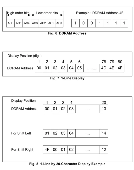
Slaver address could set from “0111100” to “0111111”.
The I2C interface send RAM data and executes the commands sent via the I2C Interface. It could send data in to the RAM. The I2C Interface is two-line communication between different ICs or modules. The two lines are a Serial Data line (SDA) and a Serial Clock line (SCL). Both lines must be connected to a positive supply via a pull-up resistor. Data transfer may be initiated only when the bus is not busy.
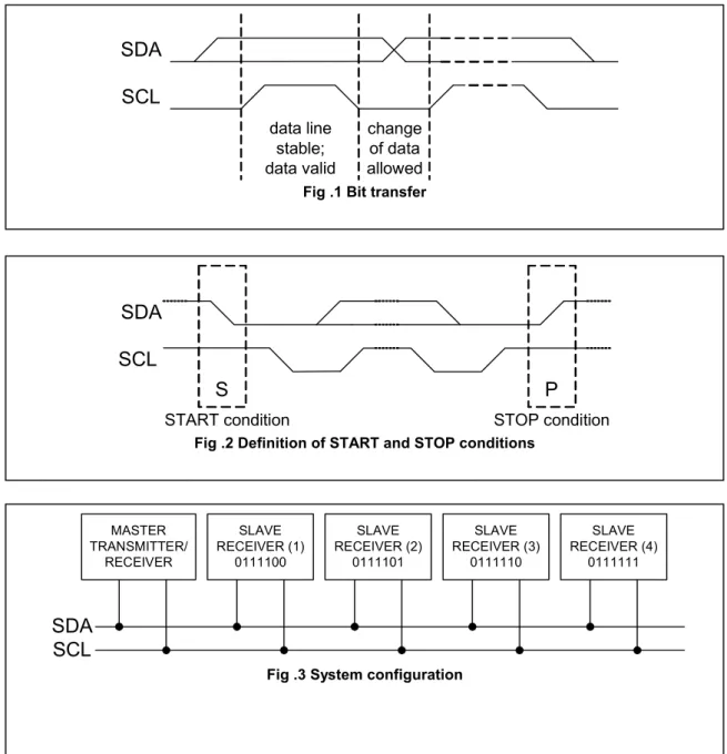
BIT TRANSFER
One data bit is transferred during each clock pulse. The data on the SDA line must remain stable during the HIGH period of the clock pulse because changes in the data line at this time will be interpreted as a control signal. Bit transfer is illustrated in Fig.1.
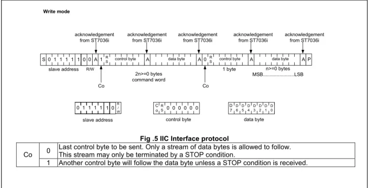
START AND STOP CONDITIONS
Both data and clock lines remain HIGH when the bus is not busy. A HIGH-to-LOW transition of the data line, while the clock is HIGH is defined as the START condition (S). A LOW-to-HIGH transition of the data line while the clock is HIGH is defined as the STOP condition (P). The START and STOP conditions are illustrated in Fig.2.
SYSTEM CONFIGURATION
RS R/W Operation
L L Instruction Write operation (MPU writes Instruction code into IR) L H Read Busy Flag(DB7) and address counter (DB0 ~ DB6) H L Data Write operation (MPU writes data into DR)
· Arbitration: procedure to ensure that, if more than one master simultaneously tries to control the bus, only one is allowed to do so and the message is not corrupted
· Synchronization: procedure to synchronize the clock signals of two or more devices.
ACKNOWLEDGE
Acknowledge signal (ACK) is not BF signal in parallel interface.
Each byte of eight bits is followed by an acknowledge bit. The acknowledge bit is a HIGH signal put on the bus by the transmitter during which time the master generates an extra acknowledge related clock pulse. A slave receiver which is addressed must generate an acknowledge after the reception of each byte. A master receiver must also generate an acknowledge after the reception of each byte that has been clocked out of the slave transmitter. The device that
acknowledges must pull-down the SDA line during the acknowledge clock pulse, so that the SDA line is stable LOW during the HIGH period of the acknowledge related clock pulse (set-up and hold times must be taken into consideration). A master receiver must signal an end-of-data to the transmitter by not generating an acknowledge on the last byte that has been clocked out of the slave. In this event the transmitter must leave the data line HIGH to enable the master to generate a STOP condition. Acknowledgement on the I2C Interface is illustrated in Fig.4.
SDA
SCL
data line stable; data valid change of data allowedFig .1 Bit transfer
SDA
SCL
S
P
START condition STOP condition
Fig .2 Definition of START and STOP conditions
MASTER TRANSMITTER/ RECEIVER SLAVE RECEIVER (1) 0111100 SLAVE RECEIVER (2) 0111101 SLAVE RECEIVER (3) 0111110 SLAVE RECEIVER (4) 0111111
SDA
SCL
I2C Interface protocol
The ST7036 supports command, data write addressed slaves on the bus.
Before any data is transmitted on the I2C Interface, the device, which should respond, is addressed first. Four 7-bit slave addresses (0111100 to 0111111) are reserved for the ST7036. The R/W is assigned to 0 for Write only.
The I2C Interface protocol is illustrated in Fig.5.
The sequence is initiated with a START condition (S) from the I2C Interface master, which is followed by the slave address. All slaves with the corresponding address acknowledge in parallel, all the others will ignore the I2C Interface transfer. After acknowledgement, one or more command words follow which define the status of the addressed slaves.
A command word consists of a control byte, which defines Co and RS, plus a data byte.
The last control byte is tagged with a cleared most significant bit (i.e. the continuation bit Co). After a control byte with a cleared Co bit, only data bytes will follow. The state of the RS bit defines whether the data byte is interpreted as a command or as RAM data. All addressed slaves on the bus also acknowledge the control and data bytes. After the last control byte, depending on the RS bit setting; either a series of display data bytes or command data bytes may follow. If the RS bit is set to logic 1, these display bytes are stored in the display RAM at the address specified by the data pointer. The data pointer is automatically updated and the data is directed to the intended ST7036i device. If the RS bit of the last control byte is set to logic 0, these command bytes will be decoded and the setting of the device will be changed according to the received commands. Only the addressed slave makes the acknowledgement after each byte. At the end of the transmission the I2C INTERFACE-bus master issues a STOP condition (P).
1 2 8 9
S
DATA OUTPUT BY TRANSMITTER DATA OUTPUT BY RECEIVER SCL FROM MASTER START condition not acknowledge acknowledgeclock pulse for acknowledgement
During write operation, two 8-bit registers are used. One is data register (DR), the other is instruction register(IR).
The data register(DR) is used as temporary data storage place for being written into DDRAM/CGRAM/ICON RAM, target RAM is selected by RAM address setting instruction. Each internal operation, writing into RAM, is done automatically. So to speak, after MPU writes data to DR, the data in DR is transferred into
DDRAM/CGRAM/ICON RAM automatically.
The Instruction register(IR) is used only to store instruction code transferred from MPU. MPU cannot use it to read instruction data.
To select register, use RS bit input in IIC interface.
Table 2. Various kinds of operations according to RS and R/W bits.
z Busy Flag (BF)
When BF = "High”, it indicates that the internal operation is being processed. So during this time the next instruction cannot be accepted. BF can be read, when RS = Low and R/W = High (Read Instruction Operation), through DB7 port. Before executing the next instruction, be sure that BF is not High.
z Address Counter (AC)
Address Counter(AC) stores DDRAM/CGRAM/ICON RAM address, transferred from IR.
After writing into (reading from) DDRAM/CGRAM/ICON RAM, AC is automatically increased (decreased) by 1. When RS = "Low" and R/W = "High", AC can be read through DB0 ~ DB6 ports.
RS R/W Operation
L L Instruction Write operation (MPU writes Instruction code into IR) H L Data Write operation (MPU writes data into DR)
S 0 1 1 1 1 1 R
S
0 A control byte A data byte
Co
0 R S
A control byte A data byte A P
Co slave address acknowledgement from ST7036i acknowledgement from ST7036i acknowledgement from ST7036i acknowledgement from ST7036i acknowledgement from ST7036i 2n>=0 bytes command word n>=0 bytes MSB...LSB 1 byte R/W Write mode C o R S 0 0 0 0 0 0 control byte D 7 D 6 D 5 D 4 D 3 D 2 D 1 D 0 data byte 1 0 0 0 1 1 1 1 R/ W 1 0 slave address
Fig .5 IIC Interface protocol
0 Last control byte to be sent. Only a stream of data bytes is allowed to follow. This stream may only be terminated by a STOP condition. Co
z Display Data RAM (DDRAM)
Display data RAM (DDRAM) stores display data represented in 8-bit character codes. Its extended capacity is 80 x 8 bits, or 80 characters. The area in display data RAM (DDRAM) that is not used for display can be used as general data RAM. See Figure 6 for the relationships between DDRAM addresses and positions on the liquid crystal display.
The DDRAM address (ADD ) is set in the address counter (AC) as hexadecimal. ¾ 1-line display (N3=0,N = 0) (Figure 7)
When there are fewer than 80 display characters, the display begins at the head position. For example, if using only the ST7036, 20 characters are displayed. See Figure 7.
When the display shift operation is performed, the DDRAM address shifts. See Figure 8.
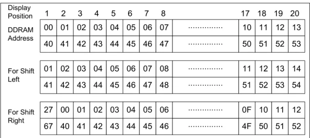
High order bits Low order bits
AC6 AC5 AC4 AC3 AC2 AC1 AC0 1 0 0 1 1 1 1
Example : DDRAM Address 4F
Display Position (digit)
Fig. 6 DDRAM Address
Fig. 7 1-Line Display
00 01 02 03 04 05 ... 4D 4E 4F
DDRAM Address
Display Position
Fig. 8 1-Line by 20-Character Display Example
DDRAM Address 00 01 02 03 .... 13 1 2 3 4 5 6 78 79 80 1 2 3 4 20 14 01 02 03 04 .... 00 01 02 .... 12 4F
For Shift Left
¾ 2-line display (N3=0,N = 1) (Figure 9)
Case 1: When the number of display characters is less than 40 x 2 lines, the two lines are displayed from the head. Note that the first line end address and the second line start address are not consecutive. For example, when just the ST7036 is used, 20 characters x 2 lines are displayed. See Figure 9.
When display shift operation is performed, the DDRAM address shifts. See Figure 10.
Fig. 9 2-Line Display
00 01 02 03 04 05 ... 25 26 27 DDRAM Address (hexadecimal) 1 2 3 4 5 6 38 39 40 Display Position 40 41 42 43 44 45 ... 65 66 67 Display Position
Fig. 10 2-Line by 20-Character Display Example
DDRAM Address For Shift Left For Shift Right 1 2 3 4 5 6 7 8 17 18 19 20 00 01 02 03 04 05 06 27 40 41 42 43 44 45 46 67 0F 10 11 12 4F 50 51 52 00 01 02 03 04 05 06 07 08 01 02 03 04 05 06 07 40 41 42 43 44 45 46 47 48 41 42 43 44 45 46 47 10 11 12 13 50 51 52 53 11 12 13 14 54 51 52 53 ……… ……… ……… ……… ……… ………
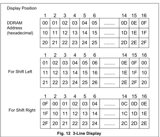
¾ 3-line display (N3=1,N =1) (Figure 11)
Case 1: When the number of display characters is less than 16 x 3 lines, the tree lines are displayed from the head. For example, when just the ST7036 is used, 16 characters x 3 lines are displayed. See Figure 11. When display shift operation is performed, the DDRAM address shifts. See Figure 12.
Fig. 12 3-Line Display
00 01 02 03 04 05 ... 0D 0E 0F DDRAM Address (hexadecimal) 1 2 3 4 5 6 14 15 16 Display Position 10 11 12 13 14 15 ... 1D 1E 1F 20 21 22 23 24 25 ... 2D 2E 2F 1 2 3 4 5 6 14 15 16
For Shift Left
For Shift Right
01 02 03 04 05 06 ... 0E 0F 00 11 12 13 14 15 16 ... 1E 1F 10 21 22 23 24 25 26 ... 2E 2F 20 0F 00 01 02 03 04 ... 0C 0D 0E 1 2 3 4 5 6 14 15 16 1F 10 11 12 13 14 ... 1C 1D 1E 2F 20 21 22 23 24 ... 2C 2D 2E
Fig. 11 3-Line Display
00 01 02 03 04 05 ... 0D 0E 0F DDRAM Address (hexadecimal) 1 2 3 4 5 6 14 15 16 Display Position 10 11 12 13 14 15 ... 1D 1E 1F 20 21 22 23 24 25 ... 2D 2E 2F
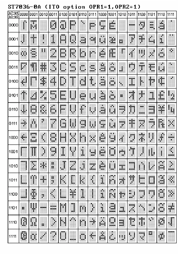
z Character Generator ROM (CGROM)
The character generator ROM generates 5 x 8 dot character patterns from 8-bit character codes. It can generate 240/250/248/256 5 x 8 dot character patterns(select by OPR1/2 ITO pin). User-defined character patterns are also available by mask-programmed ROM.
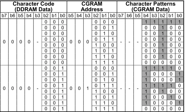
z Character Generator RAM (CGRAM)
In the character generator RAM, the user can rewrite character patterns by program. For 5 x 8 dots, eight character patterns can be written.
Write into DDRAM the character codes at the addresses shown as the left column of Table 5 to show the character patterns stored in CGRAM.
See Table 5 for the relationship between CGRAM addresses and data and display patterns. Areas that are not used for display can be used as general data RAM.
z ICON RAM
In the ICON RAM, the user can rewrite icon pattern by program. There are totally 80 dots for icon can be written.
See Table 6 for the relationship between ICON RAM address and data and the display patterns. z Timing Generation Circuit
The timing generation circuit generates timing signals for the operation of internal circuits such as DDRAM, CGROM and CGRAM. RAM read timing for display and internal operation timing by MPU access are generated separately to avoid interfering with each other. Therefore, when writing data to DDRAM, for example, there will be no undesirable interference, such as flickering, in areas other than the display area.
z LCD Driver Circuit(N3=0)
LCD Driver circuit has 17 common and 100 segment signals for LCD driving. Data from CGRAM/CGROM/ICON is transferred to 100 bit segment latch serially, and then it is stored to 100 bit shift latch. When each common is selected by 17 bit common register, segment data also output through segment driver from 100 bit segment latch. In case of 1-line display mode, COM1 ~ COM8(with COMI) have 1/9 duty, and in 2-line mode, COM1 ~ COM16(with COMI) have 1/17 duty ratio.
z LCD Driver Circuit(N3=1)
LCD Driver circuit has 25 common and 80 segment signals for LCD driving. Data from CGRAM/CGROM/ICON is transferred to 80 bit segment latch serially, and then it is stored to 80 bit shift latch. When each common is selected by 25 bit common register, segment data also output through segment driver from 80 bit segment latch. In case of 3-line display mode, COM1 ~ COM24(with COMI) have 1/25 duty.
COM/SEG Output pins
N3 COMI1 COM [1:8] SEG [1:5] [6:10]SEG [11:90] SEG [91:96] SEG [97:100] SEG [9:16] COM COMI2 VSS COMI1 COM [1:8] SEG [1:5] [6:10]SEG [11:90] SEG [91:96] SEG [97:100] SEG [9:16] COM COMI2 VDD NC [5:12] COM COM[4:1] + COMI1 NC [1:80] SEG NC [13:16] COM [17:24] COM COMI2
Table 3. COM/SEG output define z Cursor/Blink Control Circuit
It can generate the cursor or blink in the cursor/blink control circuit. The cursor or the blink appears in the digit at the display data RAM address set in the address counter.
Character Code
(DDRAM Data)
Address
CGRAM
Character Patterns
(CGRAM Data)
b7 b6 b5 b4 b3 b2 b1 b0 b5 b4 b3 b2 b1 b0 b7 b6 b5 b4 b3 b2 b1 b0 0 0 0 0 0 0 1 1 1 1 1 0 0 0 0 0 1 0 0 1 0 0 0 0 0 0 1 0 0 0 1 0 0 0 0 0 0 1 1 0 0 1 0 0 0 0 0 1 0 0 0 0 1 0 0 0 0 0 1 0 1 0 0 1 0 0 0 0 0 1 1 0 0 0 1 0 0 0 0 0 0 -0 -0 -0 0 0 0 1 1 1 - - -0 0 0 0 0 0 0 1 0 0 0 1 1 1 1 0 0 0 1 0 0 1 1 0 0 0 1 0 0 1 0 1 0 1 0 0 0 1 0 0 1 0 1 1 1 1 1 1 0 0 0 1 1 0 0 1 0 1 0 0 0 0 1 1 0 1 1 0 0 1 0 0 0 1 1 1 0 1 0 0 0 1 0 0 0 0 -0 -0 1 0 0 1 1 1 1 - - -0 0 0 0 0
Table 5 Relationship between CGRAM Addresses, Character Codes (DDRAM) and Character patterns (CGRAM Data)
Notes:
1. Character code bits 0 to 2 correspond to CGRAM address bits 3 to 5 (3 bits: 8 types).
2. CGRAM address bits 0 to 2 designate the character pattern line position. The 8th line is the cursor position and its display is formed by a logical OR with the cursor. Maintain the 8th line data, corresponding to the cursor display position, at 0 as the cursor display. If the 8th line data is 1, 1 bits will light up the 8th line regardless of the cursor presence.
3. Character pattern row positions correspond to CGRAM data bits 0 to 4 (bit 4 being at the left). 4. As shown Table 5, CGRAM character patterns are selected when character code bits 4 to 7 are all 0.
However, since character code bit 3 has no effect, the R display example above can be selected by either character code 00H or 08H.
5. “1” for CGRAM data corresponds to display selection and “0” to non-selection,“-“ Indicates no effect. 6. Different OPR1/2 ITO option can select different CGRAM size.
When SHLS=1, ICON RAM map refer below table
ICON RAM bits ICON address D7 D6 D5 D4 D3 D2 D1 D0 00H - - - S1 S2 S3 S4 S5 01H - - - S6 S7 S8 S9 S10 02H - - - S11 S12 S13 S14 S15 03H - - - S16 S17 S18 S19 S20 04H - - - S21 S22 S23 S24 S25 05H - - - S26 S27 S28 S29 S30 06H - - - S31 S32 S33 S34 S35 07H - - - S36 S37 S38 S39 S40 08H - - - S41 S42 S43 S44 S45 09H - - - S46 S47 S48 S49 S50 0AH - - - S51 S52 S53 S54 S55 0BH - - - S56 S57 S58 S59 S60 0CH - - - S61 S62 S63 S64 S65 0DH - - - S66 S67 S68 S69 S70 0EH - - - S71 S72 S73 S74 S75 0FH - - - S76 S77 S78 S79 S80
When SHLS=0, ICON RAM map refer below table
ICON RAM bits ICON address D7 D6 D5 D4 D3 D2 D1 D0 00H - - - S80 S79 S78 S77 S76 01H - - - S75 S74 S73 S72 S71 02H - - - S70 S69 S68 S67 S66 03H - - - S65 S64 S63 S62 S61 04H - - - S60 S59 S58 S57 S56 05H - - - S55 S54 S53 S52 S51 06H - - - S50 S49 S48 S47 S46 07H - - - S45 S44 S43 S42 S41 08H - - - S40 S39 S38 S37 S36 09H - - - S35 S34 S33 S32 S31 0AH - - - S30 S29 S28 S27 S26 0BH - - - S25 S24 S23 S22 S21 0CH - - - S20 S19 S18 S17 S16 0DH - - - S15 S14 S13 S12 S11 0EH - - - S10 S9 S8 S7 S6 0FH - - - S5 S4 S3 S2 S1
Table 6 ICON RAM map
Instructions
There are four categories of instructions that:
z Designate ST7036 functions, such as display format, data length, etc. z Set internal RAM addresses
z Perform data transfer with internal RAM
z Others
¾
instruction table at “Normal mode”
(when “EXT” option pin connect to VDD, the instruction set follow below table)
Instruction Code
Execution Time InstructionInstruction
RS R/W DB7 DB6 DB5 DB4 DB3 DB2 DB1 DB0Description
OSC= 380kHz OSC= 540kHz OSC= 700kHzClear
Display
0 0 0 0 0 0 0 0 0 1 Write "20H" to DDRAM. and set DDRAM address to "00H" from AC1.08 ms 0.76 ms 0.59 ms
Return
Home
0 0 0 0 0 0 0 0 1 XSet DDRAM address to "00H" from AC and return cursor to its original position if shifted. The contents of DDRAM are not changed.
1.08 ms 0.76 ms 0.59 ms
Entry Mode
Set
0 0 0 0 0 0 0 1 I/D SSets cursor move direction and specifies display shift. These operations are performed during data write and read.
26.3 µs 18.5 µs 14.3 µs
Display
ON/OFF
0 0 0 0 0 0 1 D C B D=1:entire display on C=1:cursor on B=1:cursor position on 26.3 µs 18.5 µs 14.3 µsCursor or
Display Shift
0 0 0 0 0 1 S/C R/L X X S/C and R/L:Set cursor moving and display shift control bit, and the direction, without changing DDRAM data.
26.3 µs 18.5 µs 14.3 µs
Function Set
0 0 0 0 1 DL N X X X DL: interface data is 8/4 bitsN: number of line is 2/1 26.3 µs 18.5 µs 14.3 µs
Set CGRAM
0 0 0 1 AC5 AC4 AC3 AC2 AC1 AC0Set CGRAM address in addresscounter 26.3 µs 18.5 µs 14.3 µs
Set DDRAM
Address
0 0 1 AC6 AC5 AC4 AC3 AC2 AC1 AC0 Set DDRAM address in address counter 26.3 µs 18.5 µs 14.3 µsRead Busy
Flag and
Address
0 1 BF AC6 AC5 AC4 AC3 AC2 AC1 AC0Whether during internal operation or not can be known by reading BF. The contents of address counter can also be read.
0 0 0
Write Data
to RAM
1 0 D7 D6 D5 D4 D3 D2 D1 D0 Write data into internal RAM (DDRAM/CGRAM) 26.3 µs 18.5 µs 14.3 µsRead Data
from RAM
1 1 D7 D6 D5 D4 D3 D2 D1 D0 Read data from internal RAM (DDRAM/CGRAM) 26.3 µs 18.5 µs 14.3 µsNote:
Be sure the ST7036 is not in the busy state (BF = 0) before sending an instruction from the MPU to the ST7036. If an instruction is sent without checking the busy flag, the time between the first instruction and next instruction will take much longer than the instruction time itself. Refer to Instruction Table for the list of each instruction execution time.
¾
instruction table at “Extension mode”
(when “EXT” option pin connect to VSS, the instruction set follow below table)
Instruction Code
Execution Time InstructionInstruction
RS R/W DB7 DB6 DB5 DB4 DB3 DB2 DB1 DB0Description
OSC= 380kHz OSC= 540kHz OSC= 700kHzClear
Display
0 0 0 0 0 0 0 0 0 1 Write "20H" to DDRAM. and set DDRAM address to "00H" from AC1.08 ms 0.76 ms 0.59 ms
Return
Home
0 0 0 0 0 0 0 0 1 xSet DDRAM address to "00H" from AC and return cursor to its original position if shifted. The contents of DDRAM are not changed.
1.08 ms 0.76 ms 0.59 ms
Entry Mode
Set
0 0 0 0 0 0 0 1 I/D SSets cursor move direction and specifies display shift. These operations are performed during data write and read.
26.3 µs 18.5 µs 14.3 µs
Display
ON/OFF
0 0 0 0 0 0 1 D C B D=1:entire display on C=1:cursor on B=1:cursor position on 26.3 µs 18.5 µs 14.3 µsFunction Set
0 0 0 0 1 DL N DH IS2 IS1DL: interface data is 8/4 bits N: number of line is 2/1 DH: double height font IS[2:1]: instruction table select
26.3 µs 18.5 µs 14.3 µs
Set DDRAM
Address
0 0 1 AC6 AC5 AC4 AC3 AC2 AC1 AC0 Set DDRAM address in address counter 26.3 µs 18.5 µs 14.3 µsRead Busy
Flag and
Address
0 1 BF AC6 AC5 AC4 AC3 AC2 AC1 AC0Whether during internal operation or not can be known by reading BF. The contents of address counter can also be read.
0 0 0
Write Data
to RAM
1 0 D7 D6 D5 D4 D3 D2 D1 D0 Write data into internal RAM (DDRAM/CGRAM/ICONRAM) 26.3 µs 18.5 µs 14.3 µsRead Data
Instruction table 0(IS[2:1]=[0,0])
Cursor or
Display Shift
0 0 0 0 0 1 S/C R/L X XS/C and R/L:
Set cursor moving and display shift control bit, and the direction, without changing DDRAM data.
26.3 µs 18.5 µs 14.3 µs
Set CGRAM
0 0 0 1 AC5 AC4 AC3 AC2 AC1 AC0Set CGRAM address in addresscounter 26.3 µs 18.5 µs 14.3 µs
Instruction table 1(IS[2:1]=[0,1])
Bias Set
0 0 0 0 0 1 BS 1 0 FXBS=1:1/4 bias BS=0:1/5 bias
FX: fixed on high in 3-line
application and fixed on low in other applications.
26.3 µs 18.5 µs 14.3 µs
Set ICON
Address
0 0 0 1 0 0 AC3 AC2 AC1 AC0Set ICON address in address counter. 26.3 µs 18.5 µs 14.3 µsPower/ICON
Control/
Contrast Set
0 0 0 1 0 1 Ion Bon C5 C4Ion: ICON display on/off Bon: set booster circuit on/off C5,C4: Contrast set for internal follower mode.
26.3 µs 18.5 µs 14.3 µs
Follower
Control
0 0 0 1 1 0 Fon Rab2 Rab1 Rab
0
Fon: set follower circuit on/off Rab2~0:
select follower amplified ratio.
26.3 µs 18.5 µs 14.3 µs
Contrast Set
0 0 0 1 1 1 C3 C2 C1 C0 Contrast set for internal followermode. 26.3 µs 18.5 µs 14.3 µs
Instruction table 2(IS[2:1]=[1,0])
Double
Height
Position
Select
0 0 0 0 0 1 UD X x x UD: Double height position select 26.3 µs 18.5 µs 14.3 µs
Reserved
0 0 0 1 X X X X X X Do not use (reserved for test) 26.3 µs 18.5 µs 14.3 µs
Instruction Description
z Clear Display
Clear all the display data by writing "20H" (space code) to all DDRAM address, and set DDRAM address to "00H" into AC (address counter). Return cursor to the original status, namely, bring the cursor to the left edge on first line of the display. Make entry mode increment (I/D = "1").
z Return Home
Return Home is cursor return home instruction. Set DDRAM address to "00H" into the address counter. Return cursor to its original site and return display to its original status, if shifted. Contents of DDRAM does not change.
z Entry Mode Set
Set the moving direction of cursor and display.
¾ I/D : Increment / decrement of DDRAM address (cursor or blink)
When I/D = "High", cursor/blink moves to right and DDRAM address is increased by 1. When I/D = "Low", cursor/blink moves to left and DDRAM address is decreased by 1. * CGRAM operates the same as DDRAM, when read from or write to CGRAM.
¾ S: Shift of entire display
When DDRAM read (CGRAM read/write) operation or S = "Low", shift of entire display is not performed. If S = "High" and DDRAM write operation, shift of entire display is performed according to I/D value (I/D = "1" : shift left, I/D = "0" : shift right).
S
I/D Description
H H Shift the display to the left H L Shift the display to the right
0
0
0
0
0
0
0
0
0
1
R/W
RS
DB7
DB6
DB5
DB4
DB3
DB2
DB1
DB0
0
0
0
0
0
0
0
0
1
X
R/W
RS
DB7
DB6
DB5
DB4
DB3
DB2
DB1
DB0
0
0
0
0
0
0
0
1
I/D
S
R/W
RS
DB7
DB6
DB5
DB4
DB3
DB2
DB1
DB0
z Display ON/OFF
Control display/cursor/blink ON/OFF 1 bit register.
¾ D : Display ON/OFF control bit
When D = "High", entire display is turned on.
When D = "Low", display is turned off, but display data is remained in DDRAM.
¾ C : Cursor ON/OFF control bit
When C = "High", cursor is turned on.
When C = "Low", cursor is disappeared in current display, but I/D register remains its data.
¾ B : Cursor Blink ON/OFF control bit
When B = "High", cursor blink is on, that performs alternate between all the high data and display character at the cursor position.
When B = "Low", blink is off.
z Cursor or Display Shift
¾ S/C: Screen/Cursor select bit
When S/C=”High”, Screen is controlled by R/L bit. When S/C=”Low”, Cursor is controlled by R/L bit.
¾ R/L: Right/Left
When R/L=”High”, set direction to right. When R/L=”Low”, set direction to left.
Without writing or reading of display data, shift right/left cursor position or display. This instruction is used to correct or search display data. During 2-line mode display, cursor moves to the 2nd line after 40th digit of 1st line. Note that display shift is performed simultaneously in all the line. When displayed data is shifted repeatedly, each line shifted individually. When display shift is performed, the contents of address counter are not changed.
S/C
R/L Description
AC
Value
L L Shift cursor to the left AC=AC-1 L H Shift cursor to the right AC=AC+1
Every 64 frames Alternating display Cursor
0
0
0
0
0
0
1
D
C
B
R/W
RS
DB7
DB6
DB5
DB4
DB3
DB2
DB1
DB0
0
0
0
0
0
1
S/C
R/L
X
X
R/W
RS
DB7
DB6
DB5
DB4
DB3
DB2
DB1
DB0
z Function Set
0
0 0 0 1 DL N DH IS2 IS1
R/W
RS DB7 DB6 DB5 DB4 DB3 DB2 DB1 DB0
¾ DL : Interface data length control bit
When DL = "High", it means 8-bit bus mode with MPU.
When DL = "Low", it means 4-bit bus mode with MPU. So to speak, DL is a signal to select 8-bit or 4-bit bus mode.
When 4-bit bus mode, it needs to transfer 4-bit data by two times.
¾ N : Display line number control bit
When N = "High", 2-line display mode is set. When N = "Low", it means 1-line display mode.
When “N3” option pin connect to VDD, N must set “N=1”.
¾ DH : Double height font type control bit
When DH = " High " and N= “Low”, display font is selected to double height mode(5x16 dot),RAM address can only use 00H~27H.
When DH= “High” and N= “High”, it is forbidden. When DH = " Low ", display font is normal (5x8 dot).
EXT option pin connect to
high
EXT option pin connect to
low
N DH
Display Lines
Character
Font
Display Lines
Character
Font
L L 1 5x8 1 5x8
L H 1 5x8 1 5x16
H L 2 5x8 2 5x8
H H 2 5x8 Forbidden
2 line mode normal display (DH=0/N=1)
¾ IS[2:1]: instruction table select
When IS[2:1]=(0,0): normal instruction be selected(refer instruction table 0) When IS[2:1]=(0,1):extension instruction be selected(refer instruction table 1 ) When IS[2:1]=(1,0):extension instruction be selected(refer instruction table 2 ) When IS[2:1]=(1,1):Do not use (reserved for test)
z Double height position set:IS[2:1]=(1,0)
0
0
0
0
0
1
UD
X
X
X
R/W
RS
DB7
DB6
DB5
DB4
DB3
DB2
DB1
DB0
¾ UD:Select double height font display position of screen.(N3=VDD)
When UD = "High", double height font is show on Com1~Com16.
When UD = "Low", double height font is show on Com9~Com24.
DH
UD
2 LINES(N3=VSS)
3 LINES(N3=VDD)
H H Com1~Com16 Double Height Com1~Com16 Double Height Com17~Com24 Normal Display H L Com1~Com16 Double Height Com1~Com8 Normal Display Com9~Com24 Double Height
L X Normal Display Normal Display
0
0
0
1
0
0
AC3
AC2
AC1
AC0
R/W
3 Line mode normal display (DH = 0 / N = 1 / UD = don`t care )
COM1 ..8 is normal , COM9 .. 24 is a double height font (DH = 1 / N = 1 / UD = 0 )
z Set CGRAM Address
Set CGRAM address to AC.
This instruction makes CGRAM data available from MPU.
z Set DDRAM Address
Set DDRAM address to AC.
This instruction makes DDRAM data available from MPU.
When 1-line display mode (N = 0), DDRAM address is from "00H" to "4FH".
In 2-line display mode (N = 1), DDRAM address in the 1st line is from "00H" to "27H", and DDRAM address in the 2nd line is from "40H" to "67H".
In 3-line display mode (N3=1, N=1), DDRAM address in the 1st line is from “00H” to “OFH”, DDRAM in the 2nd line is from “10H” to “1FH”, and DDRAM in the 3rd line is from “20H” to “2FH”.
z Read Busy Flag and Address
When BF = “High”, indicates that the internal operation is being processed. So during this time the next instruction cannot be accepted.
The address Counter (AC) stores DDRAM/CGRAM addresses, transferred from IR.
After writing into (reading from) DDRAM/CGRAM, AC is automatically increased (decreased) by 1.
0
0
0
1
AC5
AC4
AC3
AC2
AC1
AC0
R/W
RS
DB7
DB6
DB5
DB4
DB3
DB2
DB1
DB0
0
0
1
AC6
AC5
AC4
AC3
AC2
AC1
AC0
R/W
RS
DB7
DB6
DB5
DB4
DB3
DB2
DB1
DB0
1
0
BF
AC6
AC5
AC4
AC3
AC2
AC1
AC0
R/W
z Write Data to CGRAM,DDRAM or ICON RAM
Write binary 8-bit data to CGRAM,DDRAM or ICON RAM
The selection of RAM from DDRAM, CGRAM or ICON RAM, is set by the previous address set instruction : DDRAM address set, CGRAM address set, ICON RAM address set. RAM set instruction can also determine the AC
direction to RAM.
After write operation, the address is automatically increased/decreased by 1, according to the entry mode.
z Read Data from CGRAM,DDRAM or ICON RAM
Read binary 8-bit data from DDRAM/CGRAM./ICON RAM
The selection of RAM is set by the previous address set instruction. If address set instruction of RAM is not performed before this instruction, the data that read first is invalid, because the direction of AC is not determined. If you read RAM data several times without RAM address set instruction before read operation, you can get correct RAM data from the second, but the first data would be incorrect, because there is no time margin to transfer RAM data.
0
1
D7
D6
D5
D4
D3
D2
D1
D0
R/W
RS
DB7
DB6
DB5
DB4
DB3
DB2
DB1
DB0
1
1
D7
D6
D5
D4
D3
D2
D1
D0
R/W
RS
DB7
DB6
DB5
DB4
DB3
DB2
DB1
DB0
z Bias Set
¾ BS: bias selection
When BS=”High”, the bias will be 1/4 When BS=”Low”, the bias will be 1/5
BS will be invalid when external bias resistors are used(OPF1=1,OPF2=1)
¾ FX: must be fixed on high in 3-line application and fixed on low in other applications.
z Set ICON RAM address
Set ICON RAM address to AC.
This instruction makes ICON data available from MPU. When IS=1 at Extension mode,
The ICON RAM address is from "00H" to "0FH".
z Power/ICON control/Contrast set(high byte)
¾ Ion: set ICON display on/off
When Ion = "High", ICON display on. When Ion = "Low", ICON display off.
¾ Bon: switch booster circuit
Bon can only be set when internal follower is used (OPF1=0,OPF2=0). When Bon = "High", booster circuit is turn on.
When Bon = "Low", booster circuit is turn off.
¾ C5,C4 : Contrast set(high byte)
C5,C4,C3,C2,C1,C0 can only be set when internal follower is used (OPF1=0,OPF2=0).They can more precisely adjust the input reference voltage of V0 generator. The details please refer to the supply voltage for LCD driver.
0
0
0
1
0
1
I
ONB
ONC5
C4
R/W
z Follower control
¾ Fon: switch follower circuit
Fon can only be set when internal follower is used (OPF1=0,OPF2=0). When Fon = "High", internal follower circuit is turn on.
When Fon = "Low", internal follower circuit is turn off.
Note that Fon must be set to “Low” if (OPF1, OPF2) is not (0,0).
¾ Rab2,Rab1,Rab0 : V0 generator amplified ratio
Rab2,Rab1,Rab0 can only be set when internal follower is used (OPF1=0,OPF2=0).They can adjust the amplified ratio of V0 generator. The details please refer to the supply voltage for LCD driver.
z Contrast set(low byte)
¾ C3,C2,C1,C0:Contrast set(low byte)
C5,C4,C3,C2,C1,C0 can only be set when internal follower is used (OPF1=0,OPF2=0).They can more precisely adjust the input reference voltage of V0 generator. The details please refer to the supply voltage for LCD driver.
0
0
0
1
1
0
Rab
2
F
ONRab
0
Rab
1
R/W
RS
DB7
DB6
DB5
DB4
DB3
DB2
DB1
DB0
0
0
0
1
1
1
C3
C2
C1
C0
R/W
RS
DB7
DB6
DB5
DB4
DB3
DB2
DB1
DB0
Reset Function
Initializing by Internal Reset Circuit
An internal reset circuit automatically initializes the ST7036 when the power is turned on. The
following instructions are executed during the initialization. The busy flag (BF) is kept in the busy state (BF = 1) until the initialization ends. The busy state lasts for 40 ms after VDD rises to stable.
1. Display clear 2. Function set:
DL = 1; 8-bit interface data N = 0; 1-line display DH=0; normal 5x8 font
IS[2:1]=(0,0); use instruction table 0 3. Display on/off control:
D = 0; Display off C = 0; Cursor off B = 0; Blinking off 4. Entry mode set:
I/D = 1; Increment by 1 S = 0; No shift
5. 3 line: FX=1 1/2 line: FX=0 6. ICON control
Ion=0; ICON off 7. Power control
BS=0; 1/5bias Bon=0; booster off Fon=0; follower off
(C5,C4,C3,C2,C1,C0)=(1,0,0,0,0,0) (Rab2,Rab1,Rab0)=(0,1,0)
8. Double Height Position Select
UD=0, double height font is show on Com9~Com24.
Note:
If the electrical characteristics conditions listed under the table Power Supply Conditions Using Internal Reset Circuit are not met, the internal reset circuit will not operate normally and will fail to initialize the ST7036.
Initializing by Instruction
z 8-bit Interface (fosc=380kHz) z P O W E R O N o r e x te r n a l r e s e t W a it tim e > 4 0 m S A fte r V D D s ta b le W a it tim e > 2 6 .3μS F u n c tio n s e t R S R /W D B 7 D B 6 D B 5 D B 4 D B 3 D B 2 D B 1 D B 0 0 0 0 0 1 1 N D H IS 2 IS 1 F u n c tio n s e t R S R /W D B 7 D B 6 D B 5 D B 4 D B 3 D B 2 D B 1 D B 0 0 0 0 0 1 1 N D H IS 2 IS 1 W a it tim e > 2 6 .3μS W a it tim e > 2 6 .3μS
In itia liz a tio n e n d
B F c a n n o t b e c h e c k e d b e fo re th is in s tru c tio n . B F c a n n o t b e c h e c k e d b e fo re th is in s tru c tio n . W a it tim e > 2 6 .3μS W a it tim e > 2 6 .3μS W a it tim e > 2 6 .3μS P o w e r /IC O N /C o n tr a s t c o n tro l R S R /W D B 7 D B 6 D B 5 D B 4 D B 3 D B 2 D B 1 D B 0 0 0 0 1 0 1 Io n B o n C 5 C 4 F o llo w e r c o n tr o l R S R /W D B 7 D B 6 D B 5 D B 4 D B 3 D B 2 D B 1 D B 0 0 0 0 1 1 0 F o n R a b 2 R a b 1 R a b 0 D is p la y O N /O F F c o n tr o l R S R /W D B 7 D B 6 D B 5 D B 4 D B 3 D B 2 D B 1 D B 0 0 0 0 0 0 0 1 D C B In te r n a l O S C fr e q u e n c y R S R /W D B 7 D B 6 D B 5 D B 4 D B 3 D B 2 D B 1 D B 0 0 0 0 0 0 1 B S F 2 F 1 F 0 W a it tim e > 2 6 .3μS C o n tr a s t s e t R S R /W D B 7 D B 6 D B 5 D B 4 D B 3 D B 2 D B 1 D B 0 0 0 0 1 1 1 C 3 C 2 C 1 C 0
¾ Initial Program Code Example For 8051 MPU(8 Bit Interface):
;--- INITIAL_START:
CALL DELAY40mS
MOV A,#38H ;FUNCTION SET CALL WRINS_NOCHK ;8 bit, N=1,5*7dot CALL DELAY30uS
MOV A,#38H ;FUNCTION SET CALL WRINS_NOCHK ;8 bit, N=1,5*7dot CALL DELAY30uS
MOV A,#14H ;set bias CALL WRINS_CHK
CALL DELAY30uS
MOV A,#78H ;Contrast set adjustment CALL WRINS_CHK
CALL DELAY30uS
MOV A,#5EH ;Power/ICON/Contrast control CALL WRINS_CHK
CALL DELAY30uS
MOV A,#6AH ;Follower control CALL WRINS_CHK
CALL DELAY30uS
MOV A,#0CH ;DISPLAY ON CALL WRINS_CHK
CALL DELAY30uS
MOV A,#01H ;CLEAR DISPLAY CALL WRINS_CHK
CALL DELAY2mS
MOV A,#06H ;ENTRY MODE SET
CALL WRINS_CHK ;CURSOR MOVES TO RIGHT CALL DELAY30uS ;--- MAIN_START: XXXX XXXX XXXX XXXX ;--- WRINS_CHK: CALL CHK_BUSY WRINS_NOCHK: CLR RS ;EX: Port 3.0 CLR RW ;EX: Port 3.1 SETB E ;EX:Port 3.2
MOV P1,A ;EX:Port 1=Data Bus CLR E
MOV P1,#FFH ;For Check Busy Flag RET
;--- CHK_BUSY: ;Check Busy Flag
CLR RS SETB RW SETB E JB P1.7,$
¾ Initial Program Code Example For 8051 MPU(4 Bit Interface):
;--- INITIAL_START:
CALL DELAY40mS
MOV A,#30H ; FUNCTION SET CALL WRINS_ONCE ; 8 bit, DL = 1 CALL DELAY2mS
MOV A,#30H ; FUNCTION SET CALL WRINS_ONCE ; 8 bit, DL = 1 CALL DELAY30uS
MOV A,#30H ; FUNCTION SET CALL WRINS_ONCE ; 8 bit, DL = 1 CALL DELAY30uS
CALL CHK_BUSY
MOV A,#20H ; FUNCTION SET CALL WRINS_ONCE ; 4 bit, DL = 0 CALL DELAY30uS
MOV A,#29H ; FUNCTION SET CALL WRINS_CHK ; 4 bit, DL = 0, N = 1,
CALL DELAY30uS ; IS2 = 0, IS1 = 1
MOV A,#14H ;bias CALL WRINS_CHK
CALL DELAY30uS
MOV A,#78H ;Contrast set CALL WRINS_CHK
CALL DELAY30uS
MOV A,#5EH ;Power/ICON/Contrast
CALL WRINS_CHK CALL DELAY30uS
MOV A,#6AH ;Follower control CALL WRINS_CHK
CALL DELAY30uS
MOV A,#0CH ;DISPLAY ON CALL WRINS_CHK
CALL DELAY30uS
MOV A,#01H ;CLEAR DISPLAY CALL WRINS_CHK
CALL DELAY2mS
MOV A,#06H ;ENTRY MODE SET CALL WRINS_CHK CALL DELAY30uS XXXX ;--- WRINS_CHK: CALL CHK_BUSY WRINS_NOCHK: PUSH A ANL A,#F0H CLR RS ;EX: Port 3.0 CLR RW ;EX: Port 3.1 SETB E ;EX: Port 3.2 MOV P1,A ;EX:Port1=Data Bus CLR E POP A SWAP A WRINS_ONCE: ANL A,#F0H CLR RS CLR RW SETB E MOV P1,A CLR E
MOV P1,#FFH ;For Check Bus Flag RET
;--- CHK_BUSY: ;Check Busy Flag
PUSH A MOV P1,#FFH $1 CLR RS SETB RW SETB E MOV A,P1 CLR E MOV P1,#FFH CLR RS SETB RW SETB E NOP CLR E JB A.7,$1 POP A RET
z Serial interface & IIC interface ( fosc = 380kHz )
POWER ON and external reset
Wait time >40mS After VDD stable Wait time >26.3μS Function set RS R/W DB7 DB6 DB5 DB4 DB3 DB2 DB1 DB0 0 0 0 0 1 1 N DH IS2 IS1 Function set RS R/W DB7 DB6 DB5 DB4 DB3 DB2 DB1 DB0 0 0 0 0 1 1 N DH IS2 IS1 Wait time >26.3μS
Internal OSC frequency
RS R/W DB7 DB6 DB5 DB4 DB3 DB2 DB1 DB0
0 0 0 0 0 1 BS F2 F1 F0
Wait time >26.3μS
Display ON/OFF control
RS R/W DB7 DB6 DB5 DB4 DB3 DB2 DB1 DB0 0 0 0 0 0 0 1 D C B Initialization end Wait time >26.3μS Wait time >26.3μS Wait time >200mS (for power stable)
Power/ICON/Contrast control RS R/W DB7 DB6 DB5 DB4 DB3 DB2 DB1 DB0
0 0 0 1 0 1 Ion Bon C5 C4
Follower control
RS R/W DB7 DB6 DB5 DB4 DB3 DB2 DB1 DB0 0 0 0 1 1 0 Fon Rab2 Rab1 Rab0
Wait time >26.3μS
Contrast set
RS R/W DB7 DB6 DB5 DB4 DB3 DB2 DB1 DB0
¾ Initial Program Code Example For 8051 MPU ( Serial Interface ) :
;--- INITIAL_START:
CALL HARDWARE_RESET CALL DELAY40mS
MOV A,#38H ;FUNCTION SET CALL WRINS_NOCHK ;8 bit, N=1,5*7dot CALL DELAY30uS
MOV A,#39H ;FUNCTION SET CALL WRINS_NOCHK ;8 bit, N=1,5*7dot,IS=1 CALL DELAY30uS
MOV A,#14H ;bias CALL WRINS_NOCHK CALL DELAY30uS
MOV A,#78H ;Contrast set CALL WRINS_NOCHK
CALL DELAY30uS
MOV A,#5EH ;Power/ICON/Contrast control CALL WRINS_NOCHK
CALL DELAY30uS
MOV A,#6AH ;Follower control CALL WRINS_NOCHK
CALL DELAY200mS ;for power stable MOV A,#0CH ;DISPLAY ON CALL WRINS_NOCHK
CALL DELAY30uS
MOV A,#01H ;CLEAR DISPLAY CALL WRINS_NOCHK
CALL DELAY2mS
MOV A,#06H ;ENTRY MODE SET
CALL WRINS_NOCHK ;CURSOR MOVES TO RIGHT CALL DELAY30uS ;--- MAIN_START: XXXX XXXX XXXX XXXX . . . ;--- WRINS_NOCHK: PUSH 1 MOV R1,#8 CLR RS $1 RLC A MOV SI,C SETB SCL NOP CLR SCL
Interfacing to the MPU
The ST7036 can send data in two 4-bit operations/one 8-bit operation, serial 1 bit operation or fast I2C operation, thus allowing interfacing with 4-bit, 8-bit or I2C MPU.
z For 4-bit interface data, only four bus lines (DB4 to DB7) are used for transfer. Bus lines DB0 to DB3 are disabled. The data transfer between the ST7036 and the MPU is completed after the 4-bit data has been transferred twice. As for the order of data transfer, the four high order bits (for 8-bit operation, DB4 to DB7) are transferred before the four low order bits (for 8-bit operation, DB0 to DB3). The busy flag must be checked (one instruction) after the 4-bit data has been transferred twice. Two more 4-bit operations then transfer the busy flag and address counter data.
¾ Example of busy flag check timing sequence
¾ Intel 8051 interface(4 Bit)
Functioning DB7 Internal operation E R/W RS
Busy flag check Busy flag check Instruction write Instruction write
IR7 IR3 AC3 BusyNot AC3 IR7 IR3
CSB P1.0 to P1.3 P3.0 P3.1 P3.2 RS R/W E DB4 to DB7 COM1 to COM16/24 SEG1 to SEG100/80 100/80 16/24 Intel 8051 Serial ST7036 4 P3.3 CSB
z For 8-bit interface data, all eight bus lines (DB0 to DB7) are used.
¾ Example of busy flag check timing sequence
¾ Intel 8051 interface(8 Bit)
Data Busy Busy BusyNot Data
Functioning DB7 Internal operation E R/W RS Busy flag check Busy flag check Busy flag check Instruction write Instruction write CSB P1.0 to P1.7 P3.0 P3.1 P3.2 RS R/W E DB0 to DB7 COM1 to COM16/24 SEG1 to SEG100/80 100/80 16/24 Intel 8051 Serial ST7036 8 CSB P3.3
z4-wire SPI serial interface
¾ Example of timing sequence
¾ Intel 8051 interface ( Serial 4-line )
1 2 3 4 5 6 7 8 9 10 11 12 13 14 D7 D6 D5 D4 D3 D2 D1 D0 D7 D6 D5 D4 D3 D2
CSB
SI
SCL
RS
P1.6 to P1.7 P3.0 P3.3 RS CSB SI , SCL COM1 to COM16/24 SEG1 to SEG100/80 100/80 16/24 Intel 8051 Serial ST7036 2zI 2C interface data (ST7063i only).
¾ Example of timing sequence
¾ Intel 8051 interface ( I2C interface )
SCL
1 2 3 4 5 6 7 8 9
SDA
D7 D6 D5 D4 D3 D2 D1 D0 ACK D0 ACK. . . . . . .
Supply Voltage for LCD Drive
z When external bias resistors are used (OPF1=1,OPF2=1)
z When built-in bias resistors(9.6KΩ) are used (OPF1=1,OPF2=0) R R R GND Vext 1/5 bias VR R VDD V0 V1 V2 V3 V4 OPF1 OPF2 CAP1P CAP1N VSS VLCD VCC (2.7~ 5.5V) R R R Vext 1/4 bias R VR VDD V0 V1 V2 V3 V4 OPF1 OPF2 CAP1P CAP1N VSS VLCD GND VCC (2.7~ 5.5V) VOUT VIN VOUT VIN GND Vext VR VDD V0 V1 V2 V3 V4 OPF1 OPF2 CAP1P CAP1N VSS VLCD VCC(2.7~5.5V) VOUT VIN
z When built-in bias resistors(3.3KΩ) are used (OPF1=0,OPF2=1)
z When built-in voltage followers with external Vout are used (OPF1=0,OPF2=0 and instruction setting Bon=0,Fon=1)
GND Vext VR VDD V0 V1 V2 V3 V4 OPF2 OPF1 CAP1P CAP1N VSS VLCD VCC (2.7~ 5.5V) VOUT VIN GND VLCD VCC (2.7~ 5.5V) OPF1 OPF2 Vext ≧ V0 VDD V0 V1 V2 V3 V4 CAP1P CAP1N VSS VIN VOUT
Don't need to connect stable capacitor when use internal follower circuit
GND VDD V0 V1 V2 V3 V4 VOUT CAP1P CAP1N VSS VLCD VCC (2.7~ 3.5V) OPF1 OPF2 VOUT≦2xVDD VSS=0V VDD=2.7~3.5V
2 x step-up voltage relationships
VIN
Don't need to connect stable capacitor when use internal follower circuit
z When built-in booster and voltage followers are used(OPF1=0,OPF2=0)
Note:
Ensure V0 level stable, that must let |Vout-V0| over 0.5V(if panel size over 4.5”,the |Vout-V0| propose over 0.8V).
(System side) (ST7036Side)
Vout VDD VSS VCC GND V0 |Vout-V0|>0.5V(minimum)
¾ V0 voltage follower value calculation
C5 C4 C3 C2 C1 C0 α Rab2 Rab1 Rab0 1+Rb/Ra
0 0 0 0 0 0 0 0 0 0 1 0 0 0 0 0 1 1 0 0 1 1.25 0 0 0 0 1 0 2 0 1 0 1.5 0 1 1 1.8 : : : : 1 0 0 2 1 1 1 1 0 1 61 1 0 1 2.5 1 1 1 1 1 0 62 1 1 0 3 1 1 1 1 1 1 63 1 1 1 3.75
V0 level (Condition:Booster on, Follower on, VIN=3.5V, VDD=3.0V,Display off)
The recommended curve: follower = 04H
Notes:
1. Vout ≧V0 ≧V1 ≧V2 ≧V3 ≧V4 ≧Vss must be maintained.
Vref V0 Vout(≧VDD) VDD Ra Rb VSS ) Vref Rb Ra V0=(1+ x While Vref=VDD ( α+36 100 ) x 0 1 2 3 4 5 6 7 8 1 3 5 7 9 11 13 15 17 19 21 23 25 27 29 31 33 35 37 39 41 43 45 47 49 51 53 55 57 59 61 63
0 1 2 3 4 5 6 7 8 0 2 4 6 8 10 12 14 16 18 20 22 24 26 28 30 32 34 36 38 40 42 44 46 48 50 52 54 56 58 60 62
V0 level (Condition: VDD=5.0V, external Vout=7.0V)
The recommended curve: followe=01H
Notes:
1. Vout ≧V0 ≧V1 ≧V2 ≧V3 ≧V4 ≧Vss must be maintained.
2. If the calculation value of V0 is higher than Vout, the real V0 value will saturate to Vout. 3. internal built-in booster can only be used when OPF1=0,OPF2=0.
AC Characteristics
z
68 Interface (Ta =25°C ) VDD=2.7 to 4.5V Rating VDD=4.5 to 5.5V RatingItem Signal Symbol Condition
Min. Max. Min. Max.
Units
Address hold time RS tAH6 20 - 20 - Address setup time RS tAW6
—
20 - 20 - ns
System cycle time RS tCYC6 — 400 - 280 - ns
Data setup time D0 to D7 tDS6 100 - 80 - Data hold time D0 to D7 tDH6
—
40 - 20 - ns
Access time D0 to D7 tACC6 - 500 - 400
Output disable time D0 to D7 tOH6
CL = 100 pF
300 - 150 - ns
Enable H pulse time E tEWH — 200 - 120 - ns
tAW6 tAH6 tDS6 tDH6 tACC6 tOH6 tEWH tCYC6 tEWL RS R/W E D0 to D7 (Write) D0 to D7 (Read) CSB
z
4-wire SPI interface
(Ta = 25°C ) VDD=2.7 to 4.5V Rating VDD=4.5 to 5.5V Rating Item Signal Symbol ConditionMin. Max. Min. Max.
Units
Serial Clock Period tSCYC 200 - 100 -
SCL “H” pulse width tSHW 20 - 20 - SCL “L” pulse width SCL tSLW — 160 - 120 - ns
Address setup time tSAS 10 - 10 -
Address hold time RS tSAH — 250 - 150 - ns
Data setup time tSDS 10 - 10 -
Data hold time SI tSDH — 10 - 20 - ns
tCSS 20 - 20 -
CS-SCL time CS
tCSH — 350 - 200 - ns
*1 All timing is specified using 20% and 80% of VDD as the standard.
tCSS tCSH tSDS tSDH tSLW tSCYC tSHW RS SCL SI tSAS tSAH CSB
z I2C interface (ST7036i only) ( Ta = 25°C ) VDD=2.7 to 4.5V Rating VDD=4.5 to 5.5V Rating
Item Signal Symbol Condition
Min. Max. Min. Max.
Uni