APPLICATION
NOTE
RL78/G12
Serial Array Unit (CSI Master Communication)
Introduction
This application note describes how the serial array unit (SAU) performs communication tasks using the CSI master
communication feature. As CSI applications, the SAU selects one of two slaves with the CS signal which is issued
through a port and performs single transmission/reception, continuous transmission, continuous reception, and
continuous transmission/reception operations. To ensure reliable communication, it adopts a simple protocol and a
command set plus its compatible format. Since RL78/G12 units running in CSI slave mode are used as slave devices, it
performs handshake processing using the BUSY signal.
Target Device
RL78/G12
When applying the sample program covered in this application note to another microcomputer, modify the program
according to the specifications for the target microcomputer and conduct an extensive evaluation of the modified
program.
R01AN1369EJ0100
Rev. 1.00
Mar.01, 2013
Contents
1.
Specifications
... 3
1.1
Outline of CSI Communication
... 3
1.2
Outline of Communication
... 4
1.3
Communication Format
... 7
1.4
Communication Protocol (Hardware Handshake)
... 7
2.
Operation Check Conditions
... 8
3.
Related Application Notes
... 8
4.
Description of the Hardware
... 9
4.1
Hardware Configuration Example
... 9
4.2
List of Pins to be Used
... 10
5.
Description of the Software
... 11
5.1
Operation Outline
... 11
5.2
List of Option Byte Settings
... 13
5.3
List of Constants
... 13
5.4
List of Variables
... 15
5.5
List of Functions (Subroutines)
... 16
5.6
Function (Subroutine) Specifications
... 17
5.7
Flowcharts
... 25
6.
Changing the Channel to be Used
... 81
6.1
Definition File
... 81
6.2
Major Items of the Definition File
... 81
6.3
Changing the Transfer Rate
... 81
6.4
Changing the Microcontroller to be Used
... 81
6.5
Changing the Channel to be Used
... 82
6.6
Reference
... 83
7.
Sample Code
... 84
8.
Documents for Reference
... 84
Revision Record
... 85
1. Specifications
The serial array unit (SAU) described in this application note performs CSI master communication using the serial
array unit (SAU). The SAU outputs SPI CS signals through ports to a maximum of 2 slaves that are attached to select
the target of communication and performs single transmission/reception, continuous transmission, continuous reception,
or continuous transmission/reception while performing handshaking using the BUSY signal. (Although CS is a
negative logic signal, the bar that should normally appear over the signal name is omitted in this document.)
1.1
Outline of CSI Communication
CSI is a protocol for clock synchronous serial communication using three signal lines, namely, serial clock (SCK),
serial input data (SI), and serial output data (SO). SPI (Serial Peripheral Interface) uses an additional signal,
CS
(Chip
Select), which is used to select the slave device. The relationship among these signals is shown in figure 1.1.
SCK signal:
Clock signal for indicating the communication timing, output by the master and input to the
slaves.
SO signal:
Serial output data signal. Connected to the SI signal pin of the target device.
SI signal:
Serial input data signal. Connected to the SO signal pin of the target device.
CS signal:
Used by the master to select the target slave device.
BUSY signal: Handshake signal that is introduced by this application note.
Figure 1.1 Outline of CSI Communication
The CSI communication master first selects the slave with which it wants to communicate with the CS signal (this is an
SPI operation). The master outputs the SCK signals and place data on the SO signal line and inputs data from the SI
signal line in synchronization with the SCK signals. In CSI communication, the slave needs to become ready for
communication by the time the master starts communication (sending the SCK signals). In this application note, the
BUSY signal is introduced as the signal for indicating the slave (RL78/G12 in the example in this application note) is
ready for communication. The master verifies this BUSY signal before initiating a communication session.
Serial clock (Output)
CSI signals
RL78/G12
(Slave 1)
RL78/G12
(Master)
RL78/G12
(Slave 2)
Serial data (Output)
Serial data (Input)
Additional signal for SPI
Handshake signal
Slave select signal (Output))
SCK
SO
SI
CS
BUSY
SCK
SI
SO
CS
BUSY
SCK
SI
SO
CS
BUSY
1.2 Outline
of
Communication
Communication is performed in 1-ms slot units. In each slot, command transmission from the master and
communication processing according to the command are processed. Figure 1.2 shows the outline of slot processing
and table 1.1 lists the commands to be used.
Figure 1.2 Outline of Slots
Table 1.1 Commands to be Used
Command Outline of OperationStatus check Checks the number of data characters that the slave can transmit or receive. Receive Receives data from the slave in continuous mode.
Transmit Transmits data to the slave in continuous mode.
Transmit/receive Transmits and receives data to and from the slave in continuous mode.
The slave is designed to transmit the complement of the data it received in the next communication operation, so that
the master can determine whether the data received by the slave is correct. The master prepares increment pattern data,
e.g., 00, 01, 02, ..., as transmit data and updates the transmit data on each transmission operation.
The basic communication processing consists of subroutines that run based on interrupts. The CSI channel to be used
can be changed easily by editing a header file.
Table 1.2 lists the peripheral functions that are used and their uses. Figures 1.3 to 1.6 show the CSI communication
operations. Unless specifically noted, CSIp is represented by CSI00.
Table 1.2 Peripheral Functions to Be Used and Their Uses
Peripheral Function Use
Serial array unit m Performs CSI master communication using the SCKp signal (clock output), SIp signal (receive data), and SOp signal (transmit data).
p: 00/01/11/20
Port P23 (CS1 signal output), P22 (CS2 signal output), P21 (BUSY signal input)
20/24-pin products: m = 0, 30-pin products: m = 0/1
Slot #1
Slot #2
Slot #3
1 ms
1 ms
1 ms
Slot
Command
Communication corresponding
to the command
Space
Slot
Figure 1.3 Timing Chart of Status Check Command
Figure 1.4 Timing Chart of Receive Command
Selection of slave (start of slot)End of reception BUSY signal SCKp signal SIp signal SOp signal TSFmn INTCSIp Command transmission Data reception End of transmission
Receive command First receive data Last receive data
SIOp write Buffer empty Buffer empty SIOp read CS1/2 signal Data reception Selection of slave (start of slot)
End of reception BUSY signal SCKp signal SIp signal SOp signal TSFmn INTCSIp Command
transmission Status reception Status reception End of reception
End of transmission 00H: Status check
48H 08H
Figure 1.5 Timing Chart of Transmit Command
Figure 1.6 Timing Chart of Transmit/Receive Command
Selection of slave (start of slot)End of transfer BUSY signal SCKp signal SIp signal SOp signal TSFmn INTCSIp Command transmission Data transmission /reception Data transmission/reception End of transmission Transmit/receive command Last data First data SIOp write Buffer empty Buffer empty
Selection of slave (start of slot)
BUSY signal SCKp signal SIp signal SOp signal TSFmn INTCSIp Command transmission Data transmission Data transmission End of transmission
Transmit command First transmit data Last transmit data
SIOp write Buffer empty Buffer empty CS1/2 signal CS1/2 signal End of transmission
1.3 Communication
Format
The characteristics of the CSI communication format that is used by the sample code are listed in table 1.3.
Table 1.3 Communication Format
Item Specification Remarks Communication speed 1 Mbps About 200 kbps at minimum
Data bit length 8 bits/character Transfer order MSB first Communication type Type 1
Communication mode Single transfer/continuous transfer Continuous mode is used for data transfer.
Communication direction Receive/transmit/transmit and receive Maximum number of
characters transferred 63 characters/slot 8 characters by default
1.4 Communication
Protocol (Hardware Handshake)
The communication target is set to the RL78/G12 running in CSI slave mode and handshaking using the BUSY signal
is adopted to have the setup time that is required for the communication operation on the slave side.
The BUSY signal is used to verify that the slave becomes ready for communication when selecting it with the CS signal
or when sending a command. A timeout time of 10
s is set up so that the master does not enter an unnecessary
deadlock state when no slave is connected. If no response is returned from the slave within this period, the master
terminates processing immediately, considering that the slave is in the busy state in which it is taking some action or
that there is no slave available.
Figure 1.7 shows an example of handshaking processing for the status check command. To select the slave, the master
waits until the BUSY signal goes low while measuring the time so as to detect a timeout condition after the falling edge
of the CS signal. When the BUSY signal goes low before a timeout, the master sends the command. Upon completion
of the command transmission, the master waits until the BUSY signal goes low again to start status receive processing.
In this way, the master performs handshaking to get synchronized with the slave by checking the BUSY signal before
initiating a new communication operation.
Figure 1.7 Handshaking Example
The BUSY signal is not available for dedicated SPI slave devices such as EEPROM, A/D, and D/A. This is because
these devices are always ready for communication. A hardware measure to be taken when connecting these dedicated
slave devices is to connect the BUSY signal input to V
SS. Timeout checking is accomplished by a dedicated subroutine
(SWAITRDY). As software countermeasures, it is possible to dispense with the checking for the BUSY signal by
modifying the subroutine so that it simply returns after clearing the CY flag. Subsequently, perform communication
Selection of slave (start of slot)
End of reception BUSY signal SCKp signal TSFmn INTCSIp Command transmission
Status reception Status reception
End of reception End of transmission
Time measurement to detect timeout CS1/2 signal
2. Operation Check Conditions
The sample code contained in this application note has been checked under the conditions listed in the table below.
Table 2.1 Operation Check Conditions
Item Description Microcontroller used RL78/G12 (R5F1026A)
Operating frequency High-speed on-chip oscillator (HOCO) clock: 24 MHz CPU/peripheral hardware clock: 24 MHz
Operating voltage 5.0 V (Operation is possible over a voltage range of 2.9 V to 5.5 V.) LVD operation (VLVI): Reset mode which uses 2.81 V (2.76 V to 2.87 V) Integrated development environment CubeSuite+ V1.02.00 from Renesas Electronics Corp.
Assembler RA78K0R V1.60 from Renesas Electronics Corp. Board to be used RL78/G12 target board (QB-R5F1026A-TB)
3. Related Application Notes
The application notes that are related to this application note are listed below for reference.
RL78/G12 Initialization (R01AN1030E) Application Note
RL78/G12 Serial Array Unit (CSI Slave Communication) (R01AN1370E) Application Note
RL78 Family CubeSuite+ Startup Guide (R01AN1232E) Application Note
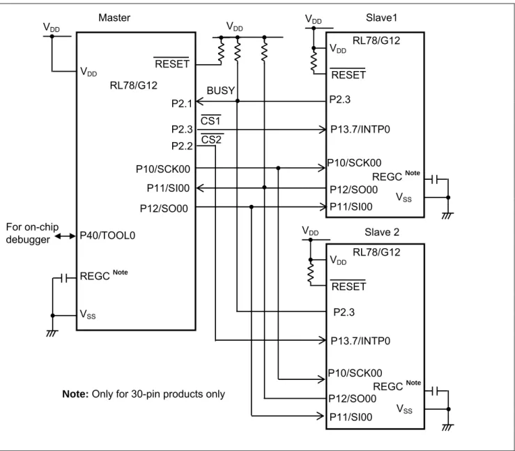
4. Description of the Hardware
4.1 Hardware
Configuration
Example
Figure 4.1 shows an example of hardware configuration that is used for this application note.
Figure 4.1 Hardware Configuration
Note: Only for 30-pin products.
Cautions: 1. The purpose of this circuit is only to provide the connection outline and the circuit is simplified
accordingly. When designing and implementing an actual circuit, provide proper pin treatment and make
sure that the hardware's electrical specifications are met (connect the input-only ports separately to V
DDor V
SSvia a resistor).
2.
V
DDmust be held at not lower than the reset release voltage (V
LVI) that is specified as LVD.
V
DDBUSY
P40/TOOL0
For on-chip
debugger
Note:
Only for 30-pin products only
Slave1
RL78/G12
V
DDV
DDP2.3
RESET
P10/SCK00
P11/SI00
P12/SO00
V
SSREGC
NoteP13.7/INTP0
Master
RL78/G12
V
DDV
DDV
SSREGC
NoteP10/SCK00
P2.1
RESET
P2.3
P2.2
P11/SI00
P12/SO00
Slave 2
RL78/G12
V
DDV
DDP2.3
RESET
P10/SCK00
P11/SI00
P12/SO00
V
SSREGC
NoteP13.7/INTP0
CS2
CS1
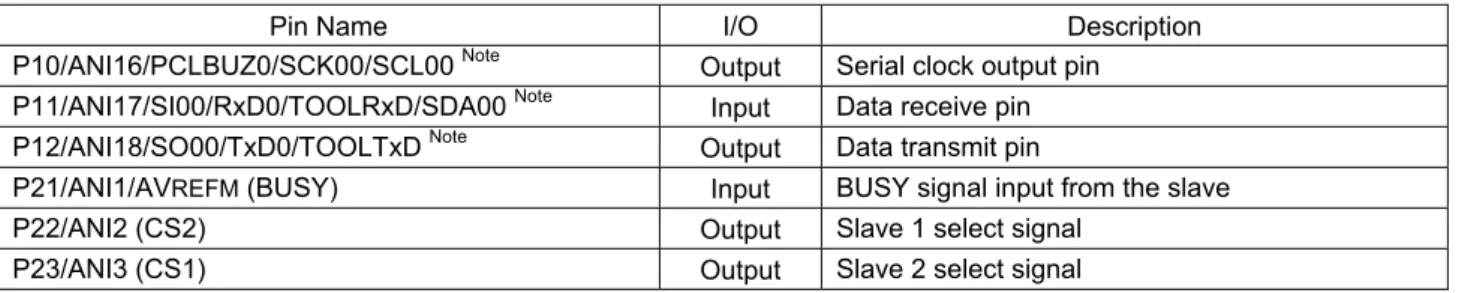
4.2
List of Pins to be Used
Table 4.1 lists the pins to be used and their function.
Table 4.1 Pins to be Used and their Functions
Pin Name I/O Description
P10/ANI16/PCLBUZ0/SCK00/SCL00 Note Output Serial clock output pin P11/ANI17/SI00/RxD0/TOOLRxD/SDA00 Note Input Data receive pin P12/ANI18/SO00/TxD0/TOOLTxD Note Output Data transmit pin
P21/ANI1/AVREFM (BUSY) Input BUSY signal input from the slave P22/ANI2 (CS2) Output Slave 1 select signal
P23/ANI3 (CS1) Output Slave 2 select signal
Note: The channel to be used must be specified in an include file (DEV&CSI_CH.inc). The default value is CSI00. The pins and interrupt to be used are automatically set according to the channel to be used.
5. Description of the Software
5.1 Operation
Outline
This sample code, after completion of initialization, selects a slave and performs communication operations such as
status check, data transmission, data transmission/reception, and data reception in that order on the selected slave.
(1) Initialize the CSI.
<Conditions for setting the CSI>
Use SAU0 channel 0 as CSI00
Note.
Use CK00 as the transfer clock.
Assign the clock output to the P10/SCK00 pin
Note, the data input to the P11/SI00 pin
Note, and the data output to
the P12/TxD0 pin
Note.
Set the data length to 8 bits.
Set the phase between the data and clock to type 1.
Set the order of data transfer mode to MSB first.
Set the transfer rate to 1M bps.
Use transmission end interrupt (INTCSI00)
Note.
Set the priority of the interrupt (INTCSI00)
Noteto the lowest (level 3 (default)).
Note: The channel to be used must be specified in an include file (DEV&CSI_CH.inc). The default value is CSI00.
The pins and interrupt to be used are automatically set according to the channel to be used.
(2) Initialize the timer.
<Conditions for setting the timer>
Run channels 3 and 2 as 8-bit interval timers.
Set the operating clock frequency to 187.5 kHz which is derived by dividing f
CLKby 128.
Use the upper TM03H as a 1-ms interval timer.
Use the lower TM03 as a 10-
s interval timer.
(3) After initialization is completed, the master initializes memory and performs communication with the slave
according to the steps given below.
1) Waits in the HALT state for 1ms interval interrupts (INTTM03H).
2) When the master is released from the HALT state on an INTTM03H interrupt, it selects (by issuing the CS
signal) the slave that is selected in the flag (RCSFLAG) and waits for a response from the slave.
3) Proceeds to step 4) when the BUSY signal from the slave goes low. When a timeout is detected, the master
deselects the slave and proceed with step 10).
4) Transmits a status check command and receives the status from the slave. When a timeout is detected, the
master deselects the slave and proceed with step 10).
5) When an INTTM03H occurs, the master transmits the number of data characters specified in step 4) and
generates the next transmit data and the expected value of the receive data. When a timeout is detected, the
master deselects the slave and proceed with step 10).
6) When an INTTM03H occurs, the master transmits and receives the number of characters specified in step 4). It
also checks whether the received data matches the complement of the data that is transmitted in step 5). When a
timeout is detected, the master deselects the slave and proceed with step 10).
7) The master generates the next transmit data and the expected value of the receive data, then waits for an
INTTM03H.
8) When an INTTM03H occurs, the master receives the number of data characters specified in step 4). When a
timeout is detected, the master deselects the slave and proceed with step 10).
9) The master checks whether the received data matches the expected value.
10) The master changes the state of the flag (RCSFLAG) to switch the target slave. Subsequently, the master repeats
the steps starting at 1).
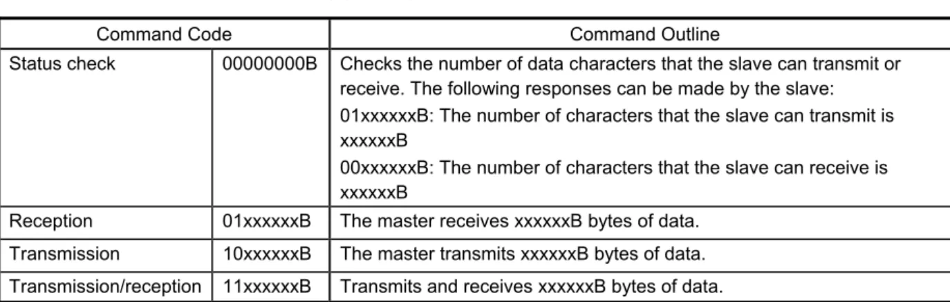
(4) Commands
Each communication operation begins with the transmission of a 1-byte command. The command formats are listed in
table 5.1. The master transmits a status check command and receives the response from the slave in the first slot of a
communication sequence. The number of received data characters or the size of buffer, whichever is smaller, is used as
the data count for the next communication processing. The master then performs the next communication using this
data count.
Table 5.1 Command Formats
Command Code Command Outline
Status check 00000000B Checks the number of data characters that the slave can transmit or receive. The following responses can be made by the slave: 01xxxxxxB: The number of characters that the slave can transmit is xxxxxxB
00xxxxxxB: The number of characters that the slave can receive is xxxxxxB
Reception 01xxxxxxB The master receives xxxxxxB bytes of data. Transmission 10xxxxxxB The master transmits xxxxxxB bytes of data. Transmission/reception 11xxxxxxB Transmits and receives xxxxxxB bytes of data.
5.2
List of Option Byte Settings
Table 5.2 summarizes the settings of the option bytes.
Table 5.2 Option Byte Settings
5.3
List of Constants
Tables 5.3 and 5.4 list the constants that are used in this sample program.
Table 5.3 Constants for the Sample Program (1/2)
Constant Defined in Setting Description CLKFREQ DEV&CSI_C
H.inc
24000 RL78/G12 operating clock frequency in kHz (24 MHz)
BAUDRATE 1000 Communication speed in kbps (1 Mbps) DIVIDE CLKFREQ / BAUDRATE Frequency division ratio necessary for attain the
specified communication speed SDRDATA (DIVIDE -1) * 200H Value to be set in SDR to specify the
communication speed INTERVAL 1 Slot interval in ms units (1 ms) TDRDATA (CLKFREQ/128) * INTERVAL - 1 Value to be set in TDR03H
SAUmEN SAU0ENSAU0EN Note SAU clock supply enable bit SPSmL SPS0LNote SAU prescaler setting register SMRmn SMR00 Note Channel mode setting register
SCRmn SCR00 Note Channel communication operation setting register SDRmn SDR00 Note Channel serial data register
SIOp SIO00 Note Lower 8 bits of channel serial data SSRmnL SSR00L Note Channel status register
SIRmnL SIR00L Note Channel flag clear trigger register SSmL SS0L Note Channel start register
STmL ST0L Note Channel stop register TRGONn 00000001B Note Value for SSmL and STmL SOEmL SOE0L Note Channel output enable register
SOEON TRGONn For setting in channel output enable register (enable)
SOEOFF 11111110B Note For setting in channel output enable register (disable)
SOm SO0 Note Channel output register
SOHIGH TRGONn For setting value in channel output register PM_CSIp PM1 Note Port mode register
PM_SCKp PM1.0 Note SCK signal port mode register PM_SIp PM1.1 Note SI signal port mode register PM_SOp PM1.2 Note SO signal port mode register
Address Value Description
000C0H 01101110B Disables the watchdog timer.
(Stops counting after the release from the reset state.) 000C1H 01111111B LVD reset mode, 2.81 V (2.76 to 2.87 V)
000C2H 11100000B HS mode, HOCO: 24 MHz 000C3H 10000101B Enables the on-chip debugger.
Table 5.4 Constants for the Sample Program (2/2)
Constant Defined In Setting Description P_CSIp DEV&CSI_CH
.inc P1 Output latch for the port to be used
P_SCKp P1.0 SCK signal port
P_SIp P1.1 SI signal port
P_SOp P1.2 SO signal port
CSIIFp CSIIF00 Channel interrupt request flag CSIMKp CSIMK00 Channel interrupt master register
CRXMODE 0100000000000111B Value to be loaded in SCR register in receive mode
CTXMODE 1000000000000111B Value to be loaded in SCR register in transmit mode
CTRXMODE 1100000000000111B Value to be loaded in SCR register in transmit/ receive mode
CSMRDATA 0000000000100000B Initial value for SMR register BUSYSIG r_main.asm P2.1 Port for checking the BUSY signal CS1SIG P2.3 CS1 output port
CS2SIG P2.2 CS2 output port
CRXDTNO 8 Size of receive data buffer (in bytes) CTXDTNO 8 Size of transmit data buffer (in bytes) STSCHKCMD 00000000B Status check command
MSTRDCMD 01000000B Master receive command MSTWTCMD 10000000B Master transmit command MSTRWOMD 11000000B Transmit/receive command SELCS1SIG 00000100B Data for selecting slave 1 SELCS2SIG 00001000B Data for selecting slave 2
5.4
List of Variables
Table 5
.
5 lists the global variables that are used in this sample program.
Table 5.5 Global Variables for the Sample Program
Type Variable Name Contents Function Used 16 bits RCSISUBADDR Address of the program that performs
actual processing when an INTCSIp interrupt occurs. main, STXDATAST, SRXDATAST, SSEQRXSUB, SSEQTXSUB, SSEQTRXSUB, IINTCSIp, STXNEXT, STRXLAST
8-bit array RSNDBUF1 Buffer for transmit data to slave 1 main, (SETTRXPNTR),
SCHANGEDATA, SSEQTXSUB, SSEQTRXSUB, STXNEXT, STRXNEXT
8-bit array RRCVBUF1 Buffer for receive data from slave 1 main, SRXNEXT, STRXNEXT, STRXEND
16 bits RSTTS1 Number of characters that can be sent to or
received from slave 1 main, SSTSCHK, STXCMD, SRXCMD, STRXCMD 8-bit array RSNDBUF2 Buffer for transmit data to slave 2 main, (SETTRXPNTR),
SCHANGEDATA, SSEQTXSUB, SSEQTRXSUB, STXNEXT, STRXNEXT
8-bit array RRCVBUF 2 Buffer for receive data from slave 2 main, SRXNEXT, STRXNEXT, STRXEND
16 bits RSTTS2 Number of characters that can be sent to or
received from slave 2 main, SSTSCHK, STXCMD, SRXCMD, STRXCMD 8 bits RCSFLAG Slave to which LSB is to access main, SETTRXPNTR,
SSLAVSEL, SSTSCHK
8 bits RRCVBUF Used to store receive data transmitted in single transfer mode.
SWAITRXEND, CSITXEND
8 bits CSISTS Number of remaining characters to be transferred STXDATAST, SWAITTXEND, SRXDATAST, SWAITRXEND, SSEQRXSUB, SWAITSTREND, SSEQTXSUB, SSEQTRXSUB, CSITXEND, SRXNEXT, STXNEXT, STXEND, STRXNEXT, STRXEND
8-bit array RCMPDATA Area for storing the expected value of the receive data
5.5
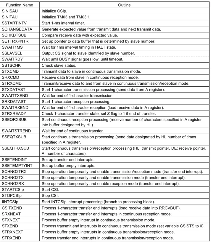
List of Functions (Subroutines)
Table 5.6 summarizes the functions (subroutines) that are used in this sample program.
Table 5.6 List of Functions (Subroutines)
Function Name Outline
SINISAU Initialize CSIp. SINITAU Initialize TM03 and TM03H. SSTARTINTV Start 1-ms interval timer.
SCHANGEDATA Generate expected value from transmit data and next transmit data. SCHKDTSUB Compare receive data with expected value.
SETTRXPNTR Set up pointer to data buffer that is determined by slave number. SWAIT1MS Wait for 1ms interval timing in HALT state.
SSLAVSEL Output CS signal to slave identified by slave number. SWAITRDY Wait until BUSY signal goes low, until timeout. SSTSCHK Check slave status.
STXCMD Transmit data to slave in continuous transmission mode. SRXCMD Receive data from slave in continuous reception mode.
STRXCMD Transmit/receive data to and from slave in continuous transmission/reception mode. STXDATAST Start 1-character transmission processing (send data from A register).
SWAITTXEND Wait for end of 1-character transmission. SRXDATAST Start 1-character reception processing.
SWAITRXEND Wait for end of 1-character reception (load receive data in A register). STRXREADY Check 1-character transfer state, set Z flag to 1 if end of transfer.
SSEQRXSUB Start continuous reception processing (receive number of characters specified in A register into buffer designated by HL).
SWAITSTREND Wait for end of continuous transfer.
SSEQTXSUB Start continuous transmission processing (send data designated by HL number of times specified in A register.
SSEQTRXSUB Start continuous transmission/reception processing (HL: transmit pointer, DE: receive pointer, A: number of characters).
SSETENDINT Set up transfer end interrupts. SSETEMPTYINT Set up buffer empty interrupts.
SCHNG2TRX Stop operation temporarily and enable transmission/reception mode (transfer end interrupt). SCHNG2TX Stop operation temporarily and enable transmission mode (transfer end interrupt).
SCHNG2RX Stop operation temporarily and enable reception mode (transfer end interrupt). STARTCSIp Start CSI.
STOPCSIp Stop CSI.
IINTCSIp Start INTCSIp interrupt processing (branch to processing block).
CSITXEND Process 1-character transfer end interrupts (load receive data into RRCVBUF). SRXNEXT Process 1-character transfer end interrupts in continuous reception mode. STXNEXT Process buffer empty interrupt in continuous transmission mode.
STXEND Process transmit end interrupts in continuous transmission mode (set variable CSISTS to 0). STRXNEXT Process buffer empty interrupts in continuous transmission/reception mode.
5.6
Function (Subroutine) Specifications
This section describes the specifications for the functions that are used in the sample program.
[Function Name] SINISAU
Synopsis Initialize CSIp.
Explanation This function sets up the CSIp for type 1, 8 bits, MSB first, and transmission/reception on transfer end interrupts.
Arguments None
Return value None Remarks None
[Function Name] SINITAU
Synopsis Initialize TM03.
Explanation This functions sets up the TM03 as two 8-bit interval timers.
Arguments None
Return value None Remarks None
[Function Name] SSTARTINTV Synopsis Start TM03H.
Explanation This functions starts the TM03H (1-ms interval timer).
Arguments None
Return value None Remarks None
[Function Name] SCHANGEDATA
Synopsis Generate expected value from transmit data and next transmit data.
Explanation This functions generates the expected value of the data to be received next from the slave from the data that has been transmitted and places the value in a variable area (RCMPDATA), then update the contents of the transmit buffer.
Arguments None
Return value None Remarks None
[Function Name] SCHKDTSUB
Synopsis Compare receive data with expected value.
Explanation This functions compares the data that is received with the expected value. The result is returned with the CY flag.
Arguments None
Return value CY flag : [1: Error detected in comparison result, 0: Comparison result is normal.] Remarks None
[Function Name] SETTRXPNTR
Synopsis Set up buffer pointer associated with selected slave.
Explanation This functions loads the address of the area containing the transmit data associated with the slave designated by RCSFLAG.0 into the HL register and the address of the buffer for storing the receive data into the DE register.
Arguments None
Return value HL register DE register
: Address for storing transmit data : Address for storing receive data Remarks None
[Function Name] SWAIT1MS
Synopsis Wait for 1-ms interval timing.
Explanation This functions disables vector interrupts and waits for the occurrence of a TM03H interrupt in HALT mode.
Arguments None
Return value None Remarks None
[Function Name] SSLAVSEL
Synopsis Perform slave selection processing.
Explanation This functions generates the CS signal to the slave designated by RCSFLAG.0 and waits for a response from the slave. When a timeout is detected, the function turns off the CS signal.
Arguments None
Return value CY flag : [1: No slave response, 0: Slave response present] Remarks None
[Function Name] SWAITRDY
Synopsis Wait response from slave.
Explanation This function starts the TM03 (for timeout measurement) and waits for a response from the slave (BUSY signal going low). When a timeout is detected before the timer startup, the function turns off the CS signal and terminates processing.
Arguments None
Return value CY flag : [1: No slave response, 0: Slave response present] Remarks None
[Function Name] IINTCSIp
Synopsis Start INTCSIp interrupt processing.
Explanation This function is activated on an INTCSIp, switches the register bank to 1, and causes a branch to the address that is stored in the variable RCSISUBADDR.
Arguments None
Return value None Remarks None
[Function Name] SSTSCHK
Synopsis Check slave status.
Explanation This function sends the Check Status command to the selected slave and stores the number of transmittable or receivable characters, which is received from the selected slave, in a work area. The function signals an error if a timeout is detected or the status (data count) that is received proves invalid.
Arguments None
Return value CY flag : [1: Invalid slave response, 0: Normal slave response] Remarks On normal execution, the function loads RSTTS1 or RSTTS2 with the numbers of
transmittable and receivable characters to and from the slave.
[Function Name] STXCMD
Synopsis Transmit data to slave.
Explanation This function sends a master transmit command to the slave, places the CSIp in transmission mode, and transmits the number of characters that the slave can receive, which is stored in RSTTS1 or RSTTS2, from the transmit data buffer.
Arguments None
Return value CY flag : [1: Invalid slave response, 0: Normal slave response] Remarks None
[Function Name] SRXCMD
Synopsis Receive data from slave.
Explanation This function sends a master receive command to the slave, places the CSIp in reception mode, and receives and stores the number of characters that the slave can transmit, which is stored in RSTTS1 or RSTTS2, into the receive data buffer.
Arguments None
Return value CY flag : [1: Invalid slave response, 0: Normal slave response] Remarks None
[Function Name] STRXCMD
Synopsis Transmit/receive data to and from slave.
Explanation This function sends a master transmit/receive command to the slave, places the CSIp in transmission/reception mode, and transmits the number of characters that the slave can transmit and receive, which is stored in RSTTS1 or RSTTS2, from the transmit data buffer and receives and stores received data in the receive data buffer.
Arguments None
Return value CY flag : [1: Invalid slave response, 0: Normal slave response]
Remarks This function is called only when the numbers of the characters that the slave can transmit and receive are the same.
The functions (subroutines) given below are available as general-purpose functions.
[Function Name] STXDATASTSynopsis Start 1-character transmission processing.
Explanation This function writes data from the A register into the SIOp and starts communication
processing. The function loads the address of CSITXEND into RCSISUBADDR as an INTCSIp processing routine and sets the number of work-in-progress characters to 1 before returning. Arguments A register Transmit data
Return value None (However, CSISTS is set to 1)
Remarks The CSIp need be configured for transmission or transmission/reception.
[Function Name] SWAITTXEND
Synopsis Wait for end of 1-character transmission.
Explanation This function waits for the end of transmission processing (CSISTS = 0) that is started by the STXDATAST function.
Arguments None
Return value None
Remarks The transmission end interrupts are processed by CSITXEND (CSISTS is set to 0).
[Function Name] SRXDATAST
Synopsis Start 1-character reception processing.
Explanation This function writes dummy data (0FFH) into the SIOp and starts receive processing. The function loads the address of CSITXEND into RCSISUBADDR as an INTCSIp processing routine and sets the number of work-in-progress characters to 1 before returning.
Arguments None
Return value None
Remarks The CSIp needs to be configured for reception or transmission/reception.
[Function Name] SWAITRXEND
Synopsis Wait for end of 1-character reception.
Explanation This function waits for the end of reception processing (CSISTS = 0) that is started by the SRXDATAST function. Upon end of reception processing, the function reads the received characters from RRCVBUF.
Arguments None
Return value A register Receive data
Remarks The receive data is stored in RRCVBUF by CSITXEND.
[Function Name] STRXREADY
Synopsis Check 1-character transfer state.
Explanation This function checks CSISTS to examine the transmission or reception state. The function returns with the Z flag set to 0 if the communication is not yet completed and with the Z flag set to 1 if the communication is completed.
Arguments None
Return value Z flag A register
: [1: Communication complete, 0: Communication in progress] : Receive data (contents of RRCVBUF) if communication is completed Remarks None
[Function Name] SSEQRXSUB
Synopsis Start continuous reception processing.
Explanation This function places the CSIp in receive mode, loads the buffer designated by the HL register with the number of characters designated by the A register, and starts reception processing. The function loads the address of SRXNEXT into RCSISUBADDR as an INTCSIp processing routine and sets the A register to the number of work-in-progress characters (CSISTS) before returning. The function returns with the Z flag set to 1 if the number of received characters in the A register is 0.
Arguments HL register A register
: Address of area for storing receive data : No of receive characters
Return value Z flag : [ 0: Normal startup, 1: Number of characters is 0.]
(CSISTS is set to the number of characters at normal startup time.) Remarks None
[Function Name] SWAITSTREND
Synopsis Wait for end of continuous transfer.
Explanation This function waits until the number of work-in-progress characters (CSISTS) reaches 0 during end of wait processing that is common to continuous reception, transmission, and
transmission/reception processing.
Arguments None
Return value None
Remarks None
[Function Name] SSEQTXSUB
Synopsis Start continuous transmission processing.
Explanation This function places the CSIp in transmission mode and starts transmission processing to send the number of characters specified in the A register from the buffer designated by the HL register. The function verifies the initiation of data transmission by testing the TSF bit. If the number of characters to be transmitted is 2 characters or more, the function changes the interrupt timing to that for buffer empty interrupts and loads RCSISUBADDR with the address of STXNEXT as an INTCSIp processing routine.
If the number of characters to be transmitted is 1 character, the function loads RCSISUBADDR with the address of STXEND.
The function returns after setting the value of the A register to the in-communication data count (CSISTS). It returns with a Z flag value of 1 if the number of receive characters in the A register is 0.
Arguments HL register A register
: Address of area for storing the transmit data : Number of characters to be transmitted Return value Z flag : [ 0: Normal startup, 1: Data count is 0.]
(CSISTS is set to the number of characters at normal startup time.) Remarks None
[Function Name] SSEQTRXSUB
Synopsis Start continuous transmission/reception processing.
Explanation This function places the CSIp in transmission/reception mode and starts the function to transmit and receive the number of data designated by the A register from the buffer
designated by the HL register. The function verifies the initiation of data transmission/reception processing by testing the TSF bit.
If the number of characters to be transmitted is 2 characters or more, the function changes the interrupt timing to that for buffer empty interrupts and loads RCSISUBADDR with the address of STRXNEXT as an INTCSIp processing routine. If the number of characters to be
transmitted is 1 character, the function loads RCSISUBADDR with the address of STRXEND. The function returns after setting the value of the A register to the in-communication data count (CSISTS). It returns with a Z flag value of 1 if the number of receive characters in the A register is 0.
Arguments HL register DE register A register
: Address of area storing the transmit data : Address of area for storing receive data : Number of transfer characters
Return value Z flag : [ 0: Normal startup, 1: Data count is 0.]
(CSISTS is set to the number of characters at normal startup time.) Remarks None
[Function Name] SSETENDINT
Synopsis Set up transfer end interrupts.
Explanation Sets the CSIp interrupt timing to end of transfer.
Arguments None
Return value None
Remarks None
[Function Name] SSETEMPTYINT
Synopsis Set up buffer empty interrupts.
Explanation Sets the CSIp interrupt timing to buffer empty interrupts.
Arguments None
Return value None
Remarks None
[Function Name] SCHNG2TRX
Synopsis Set CSIp in transmission/reception mode
Explanation This function stops the CSIp temporarily and enables the transmission/reception mode. The interrupt timing is set to end of transfer.
Arguments None
Return value None
[Function Name] SCHNG2TX
Synopsis Set CSIp in transmission mode.
Explanation This function stops the CSI temporarily and enables the transmission mode. The interrupt timing is set to end of transfer.
Arguments None
Return value None
Remarks None
[Function Name] SCHNG2RX
Synopsis Set CSIp in reception mode.
Explanation This function stops the CSI temporarily and enables the reception mode. The interrupt timing is set to end of transfer.
Arguments None
Return value None
Remarks None
[Function Name] STARTCSIp
Synopsis Enable CSIp.
Explanation This function enables the CSIp for operation.
Arguments None
Return value None
Remarks None
[Function Name] STOPCSIp
Synopsis Disable CSIp.
Explanation This function disables the CSIp.
Arguments None
Return value None
Remarks None
[Function Name] CSITXEND
Synopsis Perform 1-character transfer end interrupt processing.
Explanation This function reads receive data from the CSIp into RRCVBUF and sets the number of work-in-progress characters (CSISTS) to 0.
Arguments None
Return value None
[Function Name] SRXNEXT
Synopsis Perform 1-character transfer end interrupt processing in continuous reception mode. Explanation This function reads receive data from the CSIp into the buffer area and decrements the
number of characters (CSISTS) by 1. If the number of remaining characters is 2 or more, the function writes dummy data into the SIOp to start the receive function. If the number of remaining characters is 1, the function switches the interrupt timing to transfer end interrupt. The function terminates processing when the number of reaming characters is 0.
Arguments None
Return value None
Remarks None [Function Name] STXNEXT
Synopsis Perform buffer empty interrupt processing in continuous transmission mode.
Explanation If the number of remaining characters is 1, this function switches the interrupt timing to transfer end interrupt and changes the value of RCSISUBADDR to the address of STXEND as an INTCSIp processing routine.
If the number of remaining characters is 2 or more, the function decrements the number of work-in-progress characters (CSISTS) by 1 and writes the data from the transmit data buffer into the SIOp.
Arguments None
Return value None
Remarks None [Function Name] STXEND
Synopsis Perform transmit end interrupt processing in continuous transmission mode.
Explanation This function performs transmit end interrupt processing in continuous transmission mode. The function sets the number of work-in-progress characters (CSISTS) to 0 to signals the end of communication.
Arguments None
Return value None
Remarks None [Function Name] STRXNEXT
Synopsis Perform buffer empty interrupt processing in continuous transmission/reception mode. Explanation This function stores the receive data in the receive data buffer. If the number of remaining
characters is 2 or more, this function decrements the number of work-in-progress characters (CSISTS) by 1 and writes the data from the transmit data buffer into the SIOp.
If the number of remaining characters is 1, the function switches the interrupt timing to transfer end interrupt and changes the value of RCSISUBADDR to the address of STRXEND as an INTCSIp processing routine.
Arguments None
Return value None
Remarks None [Function Name] STRXEND
Synopsis Perform transfer end interrupt processing in continuous transmission/reception mode. Explanation This function performs transfer end interrupt processing in continuous transmission/reception
mode. The function stores the receive data in the receive data buffer and sets the number of work-in-progress characters (CSISTS) to 0 to signal the end of communication.
Arguments None
Return value None
5.7 Flowcharts
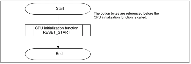
Figure 5.1 shows the overall flow of the sample program described in this application note.
Figure 5.1 Overall Flow
Start
End
The option bytes are referenced before the CPU initialization function is called.
CPU initialization function
RESET_START
5.7.1
CPU Initialization Function
Figure 5.2 shows the flowchart for the CPU initialization function.
Figure 5.2 CPU Initialization Function
RESET_START
Set up ES register
Set up stack pointer
Set up redirection
Set up I/O ports
SINIPORT
Set up clock generation
circuit SINICLK
Set up TAU
SINITAU
Set up SAU
SINISAU
Call main routine
routine
HALT
Select HOCO (24 MHz) as an operation clock.
PIOR 00H
ES 00H (for table reference)
Set CSI mode to type 1, 1 Mbps, transmission/reception, 8 bits and MSB first.
Set TM03 to 8-bit interval timer. P1 (CSI00 pin) 00000111B Leave P10 to P12 as input.
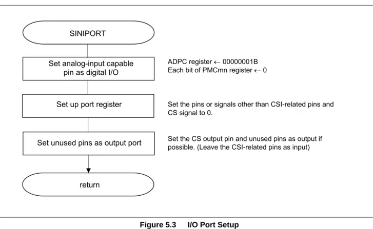
5.7.2
I/O Port Setup
Figure 5.3 shows the flowchart for I/O port setup.
Figure 5.3 I/O Port Setup
Note: Refer to the section entitled "Flowcharts" in RL78/G12 Initialization Application Note (R01AN1030E) for the
configuration of the unused ports.
Caution: Provide proper treatment for unused pins so that their electrical specifications are observed. Connect each of
any unused input-only ports to V
DDor V
SSvia separate resistors.
SINIPORT
return
Set analog-input capable
pin as digital I/O
ADPC register 00000001B Each bit of PMCmn register 0
Set up port register
Set the pins or signals other than CSI-related pins and CS signal to 0.Set the CS output pin and unused pins as output if possible. (Leave the CSI-related pins as input)
5.7.3
Clock Generation Circuit Setup
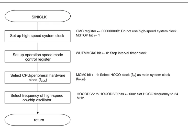
Figure 5.4 shows the flowchart for clock generation circuit setup.
Figure 5.4 Clock Generator Circuit Setup
Caution: For details on the procedure for setting up the clock generation circuit (SINICLK), refer to the section
entitled "Flowcharts" in RL78/G12 Initialization Application Note (R01AN1030E).
SINICLK
return
Set up high-speed system clock
CMC register 00000000B: Do not use high-speed system clock. MSTOP bit 1
Select CPU/peripheral hardware
clock (f
CLK)
MCM0 bit 1: Select HOCO clock (fIH) as main system clock (fMAIN).
WUTMMCK0 bit 0: Stop interval timer clock.
Select frequency of high-speed
on-chip oscillator
HOCODIV2 to HOCODIV0 bits 000: Set HOCO frequency to 24 MHz.
Set up operation speed mode
control register
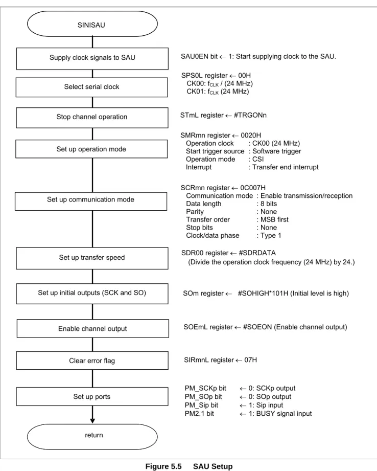
5.7.4 SAU
Setup
Figure 5.5 shows the flowchart for SAU setup.
Figure 5.5 SAU Setup
SINISAUSupply clock signals to SAU
Select serial clock
Stop channel operation
Set up communication mode
SAU0EN bit 1: Start supplying clock to the SAU. SPS0L register 00H
CK00: fCLK / (24 MHz) CK01: fCLK (24 MHz)
SMRmn register 0020H
Operation clock : CK00 (24 MHz) Start trigger source : Software trigger Operation mode : CSI
Interrupt : Transfer end interrupt STmL register #TRGONn
Set up operation mode
SCRmn register 0C007H
Communication mode : Enable transmission/reception Data length : 8 bits
Parity : None Transfer order : MSB first Stop bits : None Clock/data phase : Type 1 Set up transfer speed SDR00 register #SDRDATA
(Divide the operation clock frequency (24 MHz) by 24.)
Set up initial outputs (SCK and SO) SOm register #SOHIGH*101H (Initial level is high)
SOEmL register #SOEON (Enable channel output) Enable channel output
SIRmnL register 07H Clear error flag
return
PM_SCKp bit 0: SCKp output PM_SOp bit 0: SOp output PM_Sip bit 1: Sip input
PM2.1 bit 1: BUSY signal input Set up ports
Caution: For details on the register setup procedures, refer to RL78/G12 User's Manual: Hardware.
Symbol: SPSm
15 14 13 12 11 10 9 8 7 6 5 4 3 2 1 0 0 0 0 0 0 0 0 0 PRS m13 PRS m12 PRS m11 PRS m10 PRS m03 PRS m02 PRS m01 PRS m00 0 0 0 0 0 0 0 0 0 0 0 0 0 1 0 0Bits 7 to 0
PRS mn3 PRS mn2 PRS mn1 PRS mn0Selection of operation clock (CK0n) (n = 0 to 1)
fCLK = 2 MHz fCLK = 5 MHz fCLK = 10 MHz fCLK = 20 MHz fCLK = 24 MHz 0 0 0 0 fCLK 2 MHz 5 MHz 10 MHz 20 MHz 24 MHz 0 0 0 1 fCLK/2 1 MHz 2.5 MHz 5 MHz 10 MHz 12 MHz 0 0 1 0 fCLK/22 500 kHz 1.25 MHz 2.5 MHz 5 MHz 6 MHz 0 0 1 1 fCLK/23 250 kHz 625 kHz 1.25 MHz 2.5 MHz 3 MHz 0 1 0 0 fCLK/24 125 kHz 313 kHz 625 kHz 1.25 MHz 1.5 MHz 0 1 0 1 fCLK/25 62.5 kHz 156 kHz 313 KHz 625 KHz 750 kHz 0 1 1 0 fCLK/26 31.3 kHz 78.1 kHz 156 kHz 313 kHz 375 kHz 0 1 1 1 fCLK/27 15.6 kHz 39.1 kHz 78.1 kHz 156 kHz 188 kHz 1 0 0 0 fCLK/28 7.81 kHz 19.5 kHz 39.1 kHz 78.1 kHz 93.8 kHz 1 0 0 1 fCLK/29 3.91 kHz 9.77 kHz 19.5 kHz 39.1 kHz 46.9 kHz 1 0 1 0 fCLK/210 1.95 kHz 4.88 kHz 9.77 kHz 19.5 kHz 23.4 kHz 1 0 1 1 fCLK/211 977 Hz 2.44 kHz 4.88 kHz 9.77 kHz 11.7 kHz 1 1 0 0 fCLK/212 488 Hz 1.22 kHz 2.44 kHz 4.88 kHz 5.86 kHz 1 1 0 1 fCLK/213 244 Hz 610 Hz 1.22 kHz 2.44 kHz 2.93 kHz 1 1 1 0 fCLK/214 122 Hz 305 Hz 610 Hz 1.22 kHz 1.46 kHz 1 1 1 1 fCLK/215 61 Hz 153 Hz 305 Hz 610 Hz 732 Hz
Peripheral enable register 0 (PER0)
Start supplying clock signals.
Starting clock signal supply to SAU
Serial clock select register m (SPSm)
Select an operation clock for SAU.
Selecting a serial clock
Symbol: PER0
7 6 5 4 3 2 1 0
TMKAE 0 ADCEN IICA0EN SAU1EN SAU0EN 0 TAU0EN
x 0 x x 0/1 0/1 0 x
Bits 3 and 2
SAUmEN Control of serial array unit n input clock supply
0 Stops supply of input clock. 1 Enables supply of input clock.
Symbol: SMRmn
15 14 13 12 11 10 9 8 7 6 5 4 3 2 1 0 CKS mn CCS mn 0 0 0 0 0 STS mn 0 0 1 0 0 MD mn2 MD mn1 MD mn0 0 0 0 0 0 0 0 0 0 0 1 0 0 0 0 0Bit 15
CKSmn Selection of operation clock (fMCK) of channel n
0 Prescaler output clock CK00 set by the SPSm register
1 Prescaler output clock CK01 set by the SPSm register
Bit 14
CCSmn Selection of transfer clock (TCLK) of channel n
0 Divided operation clock fMCK set by the CKSmn bit 1 Clock input from the SCK pin.
Bit 8
STSmn Selection of start trigger source
0 Only software trigger is valid
1 Valid edge of the RxD pin (selected for UART reception)
Bits 2 and 1
MDmn2 MDmn1 Setting of operation mode of channel n
0 0 CSI mode
0 1 UART mode
1 0 Simplified I2C mode 1 1 Setting prohibited
Bit 0
MDmn0 Selection of interrupt source of channel n
0 Transfer end interrupt
1 Buffer empty interrupt
Caution: For details on the register setup procedures, refer to RL78/G12 User's Manual: Hardware.
Serial mode register mn (SMRmn)
Interrupt source
Operation mode
Select transfer clock.
Select f
MCK.Symbol: SCRmn
15 14 13 12 11 10 9 8 7 6 5 4 3 2 1 0 TXE mn RXE mn DAP mn CKP mn 0 EOC mn PTC mn1 PTC mn0 DIR mn 0 SLC mn1 SLC mn0 0 1 DLS mn1 DLS mn0 1 1 0 0 0 0 0 0 0 0 0 0 0 1 1 1Bits 15 and 14
TXEmn RXEmn Setting of operation mode of channel n 0 0 Disable communication.
0 1 Reception only
1 0 Transmission only
1 1 Transmission/reception
Bit 10
EOCmn Selection of masking of error interrupt signal (INTSREn)
0 Masks error interrupt INTSRE0.
1 Enables generation of error interrupt INTSREx.
Bits 9 and 8
PTCmn 1
PTCmn 0
Setting of parity bit in UART mode
Transmission Reception
0 0 Does not output the parity bit. Receives without parity.
0 1 Outputs 0 parity. No parity judgment 1 0 Outputs even parity. Judged as even parity 1 1 Outputs odd parity. Judged as odd parity
Bit 7
DIRmn Selection of data transfer sequence in CSI and UART modes
0 Inputs/outputs data with MSB first.
1 Inputs/outputs data with LSB first.
Bits 5 and 4
SLCmn 1
SLCmn
0 Setting of stop bit in UART mode
0 0 No stop bit
0 1 Stop bit length = 1 bit 1 0 Stop bit length = 2 bits 1 1 Setting prohibited
Caution: For details on the register setup procedures, refer to RL78/G12 User's Manual: Hardware.
Serial communication operation register mn (SCRmn)
Setup data length, data transfer order, and operation mode.
Setting up channel communication mode
Caution: For details on the register setup procedures, refer to RL78/G12 User's Manual: Hardware.
Symbol: SCRmn
15 14 13 12 11 10 9 8 7 6 5 4 3 2 1 0 TXE mn RXE mn DAP mn CKP mn 0 EOC mn PTC mn1 PTC mn0 DIR mn 0 SLC mn1 SLC mn0 0 1 DLS mn1 DLS mn0 1 1 0 0 0 0 0 0 0 0 0 0 0 1 1 1Bits 1 and 0
DLSmn 1 DLSmn0 Setting of data length in CSI mode 0 1 9-bit data length
1 0 7-bit data length
1 1 8-bit data length
Other than
above Setting prohibited
Symbol: SDRmn
15 14 13 12 11 10 9 8 7 6 5 4 3 2 1 0
0 0 1 0 1 1 1 0 x x x x x x x x
Bits 15 to 9
SDRmn[15:9] Transfer clock setting by dividing operation clock (fMCK)
0 0 0 0 0 0 0 fMCK /2 0 0 0 0 0 0 1 fMCK /4 0 0 0 0 0 1 0 fMCK /6 0 0 0 0 0 1 1 fMCK /8 0 0 1 0 1 1 1 fMCK /24 1 1 1 1 1 1 0 fMCK /254 1 1 1 1 1 1 1 fMCK /256
Serial data register mn (SDRmn)
Transfer clock frequency: f
MCK/24 (= 1 MHz)
Caution: For details on the register setup procedures, refer to RL78/G12 User's Manual: Hardware.
Symbol: SOm
15 14 13 12 11 10 9 8 7 6 5 4 3 2 1 0 0 0 0 0 CKO m3 CKO m2 CKO m1 CKO m0 0 0 0 0 SO m3 SO m2 SO m1 SO m0 0 0 0 0 0/1 0/1 0/1 0/1 0 0 0 0 0/1 0/1 0/1 0/1Bit n
SOmn Serial clock output of channel n 0 Serial data output value is “0”.
1 Serial data output value is “1”.
Serial output register m (SOm)
Initial output: 1
Setting initial output level
Symbol: SOEm
15 14 13 12 11 10 9 8 7 6 5 4 3 2 1 0 0 0 0 0 0 0 0 0 0 0 0 0 SOE m3 SOE m2 SOE m1 SOE m0 0 0 0 0 0 0 0 0 0 0 0 0 0/1 0/1 0/1 0/1Bit n
SOEmn Serial output enable/disable of channel n 0 Disables output by serial communication operation.
1 Enables output by serial communication operation.
Serial output enable register m (SOEm/SOEmL)
Enable output
Enabling target channel data output
Caution: For details on the register setup procedures, refer to RL78/G12 User's Manual: Hardware.
Symbol: SIRmn
15 14 13 12 11 10 9 8 7 6 5 4 3 2 1 0 0 0 0 0 0 0 0 0 0 0 0 0 0 FECT mn PECT mn OVCT mn 0 0 0 0 0 0 0 0 0 0 0 0 0 1 1 1Bit 2
FECTmn Clear trigger of framing error of channel n 0 Not cleared
1 Clears the FEFmn bit of the SSRmn registers to 0.
Bit 1
PECTmn Clear trigger of parity error of channel n 0 Not cleared
1 Clears the PEFmn bit of the SSRmn registers to 0.
Bit 0
OVCTmn Clear trigger of overrun error of channel n 0 Not cleared
1 Clears the OVFmn bit of the SSRmn registers to 0.
Serial flag clear trigger register mn (SIRmn)
Clear the error flags
Clearing the error flags
Symbol: MK0H (20-/24- pin products)
7 6 5 4 3 2 1 0 TMMK01 TMMK00 IICAMK0 TMMK 03H TMMK 01H SREMK0 SRMK0 CSIMK01 IICMK01 STMK0 CSIMK00 IICMK00 x x x x x x 0/1 0/1
CSIMK01 CSIMK00 Interrupt processing control
0 0 Enables interrupt processing.
1 1 Disables interrupt processing.
Interrupt mask flag register 0H (MK0H)
Disable interrupt processing.
Caution: For details on the register setup procedures, refer to RL78/G12 User's Manual: Hardware.
Port register 1 (P1)
Port mode register 1 (PM1)
Port setting for each of serial clock, transmit data and receive data.
Symbol: P1
7 6 5 4 3 2 1 0 P17 P16 P15 P14 P13 P12 P11 P10 x x x x x 1 1 1Bit 2
P12 toP10 Output data control (in output mode) 0 0 is output
1 1 is output
Port setting (For CSI00)
Symbol: PM1
7 6 5 4 3 2 1 0 PM17 PM16 PM15 PM14 PM13 PM12 PM11 PM10
x x x x x 0 1 0
Bit 2
PM12 P12 pin I/O mode selection
0 Output mode (output buffer on)
1 Input mode (output buffer off)
Bit 1
PM11 P11 pin I/O mode selection 0 Output mode (output buffer on)
1 Input mode (output buffer off)
Bit 0
PM10 P10 pin I/O mode selection
0 Output mode (output buffer on)
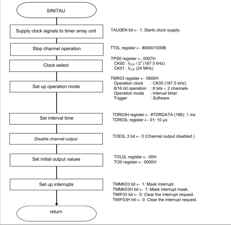
5.7.5
Timer Array Unit Setup
Figure 5.6 shows the flowchart for setting up the timer array unit.
Figure 5.6 Timer Array Unit Setup
SINITAU
Supply clock signals to timer array unit
Clock select
Stop channel operation
Set interval time
TAU0EN bit 1: Starts clock supply.
TPS0 register 0007H CK00 : fCLK / 27 (187.5 kHz) CK01 : fCLK (24 MHz) TMR03 register 0800H
Operation clock : CK00 (187.5 kHz) 8/16 bit operation : 8 bits 2 channels Operation mode : Interval timer Trigger : Software TT0L register #00001000B
Set up operation mode
TDR03H register #TDRDATA (186): 1 ms TDR03L register 01: 10 μs
Set initial output values
TOL0L register TO0 register 0000H 00HTOE0L.3 bit 0 (Channel output disabled.) Disable channel output
TMMK03 bit 1: Mask interrupt. TMMK03H bit 1: Mask interrupt mask. TMIF03 bit 0: Clear the interrupt request. TMIF03H bit 0: Clear the interrupt request.
Set up interrupts
5.7.6 Main
Processing
Figures 5.7 to 5.9 show the flowcharts for the main processing.
Figure 5.7 Main Processing (1/3)
main
Enable vector interrupts
Start 1-ms interval timer.
IE 1: Enable vector interrupts
Start 1-ms timer
SSTARTINTV
Initialize data buffers
Initialize data buffers.
RRCVBUF1/2 00: Clear receive buffer with 00H. RSNDBUF1/2 00: Initialize transmit buffer with incrementing data.
RSTTS1/2 0000H: Clear slave status .
Disable the TM03H for 1-ms interval vector interrupts and wait in the HALT state.
Wait for 1 ms
SWAIT1MS
READY response?
Yes No
Send a status check command to the selected slave and receive the number of transmittable/receivable characters.
Status check command
SSTSCHK
Terminate processing and cause a branch if a timeout occurs.
Transmit command
STXCMD
Perform transmit command processing. Enable CSIp and unmask interrupts.
Enable CSIp
STARTCSIp
A
Output the CS signal designated by the RCSFLAG.0 bit to the slave and wait until the BUSY signal goes low.
Select slave
!SSLAVSEL
D Yes NoNormal response?
Yes NoNormal end?
BTerminate processing and cause a branch if an abnormal response is received from the slave.
Terminate processing and cause a branch if an abnormal response is received from the slave.
Check transmit/receive data count
Get the pointer to the target slave.
Check if the slave's transmittable data count and receivable data count match.
Get pointer
SETTRXPNTR
RCMPDATA Expected value of response for previously transmitted data
RSNDBUF1/2 Next transmit data (continued from preceding data)
Data count match?
Yes
No Cause a branch to receive command if the data counts disagree.
Perform transmit/receive command processing.
Data transmit/receive
command
STRXCMD
Normal end? Yes NoEnter the HALT mode if the value of the received data does not match the expected value.
Check if the value of received data matches the expected value.
B
Update data
SCHANGEDATA
D
Check receive data
SCHKDTSUB
HALT
Data mismatch?
Yes No
RCMPDATA Expected value of response for the previously transmitted data
RSNDBUF1/2 Next transmit data (continued from preceding data)
Update data
SCHANGEDATA
Perform receive command processing.
Data receive command
SRXCMD
Figure 5.9 Main Processing (3/3)
Check if the value of received data matches the expected value.
Normal end?
Yes No
Invert the RCSFLAG.0 bit identifying the slave and continue processing starting at the status check step.
Data mismatch?
Yes No
Change slave
C
Check receive data
SCHKDTSUB
D
Enter the HALT mode if the value of the received data does not match the expected value.
HALT
5.7.7
1-ms Interval Timer Startup Processing
Figure 5.10 shows the flowchart for the 1-ms interval timer startup function.
Figure 5.10 1-ms Interval Timer Startup Processing
Caution: For details on the register setup procedures, refer to RL78/G12 User's Manual: Hardware.
SSTARTINTV
Enable TM03H
Set up the TS0 register to place the TM03H in operating state.
TSH03 bit 1: Put TM03H in operating state. Clear the interrupt request flag register for the TM03H. TMIF03H bit 0: Clear interrupt request.
Enable TM03H interrupts
Clear interrupt request flag
Enable interrupts to check 1ms intervals. TMMK03H bit 0: Enable TM03H interrupts.
return
Timer channel startup register 0 (TS0)
Start counting.
Transiting to timer operating state (20-/24-pin products)
Symbol: TS0 (20-/24-pin products)
15 14 13 12 11 10 9 8 7 6 5 4 3 2 1 0
0 0 0 0 TSH03 0 TSH01 0 0 0 0 0 TS03 TS02 TS01 TS00
0 0 0 0 1 0 x 0 0 0 0 0 0 x x x
Bit 11
TSH03 Operation start trigger of channel 03H 0 No trigger operation
Caution: For details on the register setup procedures, refer to RL78/G12 User's Manual: Hardware.
Symbol: IF0H (20-/24- pin products)
7 6 5 4 3 2 1 0 TMIF01 TMIF00 IICAIF0 TMIF03H TMIF01H SREIF0
SRIF0 CSIIF01 IICIF01 STIF0 CSIIF00 IICIF00 x x x 0 x x x x
TMIF03H Interrupt request flag
0 No interrupt request signal is generated
1 Interrupt request is generated, interrupt request status
Interrupt request flag register (IF0H)
Clear the interrupt request flag
Interrupt mask flag register (MK0H)
Cancel interrupt mask
Interrupt setting
Symbol: MK0H (20-/24- pin products)
7 6 5 4 3 2 1 0 TMMK01 TMMK00 IICAMK0 TMMK03H TMMK01H SREMK0 SRMK0 CSIMK01 IICMK01 STMK0 CSIMK00 IICMK00 x x x 0 x x x x
TMMK03H Interrupt processing control
0 Enables interrupt processing.
5.7.8
1-ms Interval Wait Function
Figure 5.11 shows the flowchart for the 1ms interval wait function.
Figure 5.11 1-ms Interval Wait Function
SWAIT1MS
Save PSW in stack
Save the contents of the PSW register in the stack to manipulate the IE bit. Disable vector interrupts to use the INTTM03H only to cancel the HALT mode.Clear the INTTM03H interrupt request that cancelled the HALT mode.
TMIF03H bit 0
Unmask the interrupt mask to cancel the HALT mode. TMMK03H bit 0
Clear TM03H interrupt request
Mask on TM03H interrupt
Disable (mask) INTTM03H interrupts. TMMK03H bit 1: Disable INTTM03H.Restore the data of the PSW from the stack. (This resets the IE bit value.)
Restore PSW
Disable vector interrupts
Unmask TM03H interrupt
Transition to HALT mode
Wait for an INTM03H in HALT mode.Clear TM03H interrupt request
Clear the TMIF03H bit for timing measurement.TMIF03H bit 0
return
Cancel the HALT mode on an 1ms interval INTTM03H interrupt.
Caution: For details on the register setup procedures, refer to RL78/G12 User's Manual: Hardware.
Symbol: IF0H (20-/24- pin products)
7 6 5 4 3 2 1 0 TMIF01 TMIF00 IICAIF00 TMIF03H TMIF01H SREIF0
SRIF0 CSIIF01 IICIF01 STIF0 CSIIF00 IICIF00 x x x 0 x x x x
Bit 4
TMIF03H Interrupt request flag
0 No interrupt request signal is generated
1 Interrupt request is generated, interrupt request status
Symbol:: MK0H (20-/24- pin products)
7 6 5 4 3 2 1 0 TMMK01 TMMK00 IICAMK00 TMMK03H TMMK01H SREMK0 SRMK0 CSIMK01 IICMK01 STMK0 CSIMK00 IICMK00 x x x 0/1 x x x x
Bit 4
TMMK03H Interrupt processing control
0 Enables interrupt processing.
1 Disables interrupt processing.
Interrupt request flag register (IF0H)
Clear the interrupt request flag
Interrupt mask flag register (MK0H)
Cancel interrupt mask
5.7.9
Slave Selection Processing
Figure 5.12 shows the flowchart for the slave selection processing.
Figure 5.12 Slave Selection Processing
SSLAVSEL
Read slave number
Count up the data count (RDATACNT) (+1).
SWAITRDY
Drive the CS2 signal to the low level. P2 register #SELCS2SIG (00001000B)
Output CS2 signal
Output CS1 signal
Slave number to select is 2?
Yes No
Read the number of the slave to select from the variable RCSFLAG.
CY bit RCSFLAG.0 bit
Drive the CS1 signal to the low level. P2 register #SELCS1SIG (00000100B)