Figure 1. THAT1570 Block Diagram
FEATURES
y
Low Noise:
1 nV/
√
Hz input noise (60 dB gain)
y
Low THD+N:
0.0003%
≤
30 dB gain
0.0008% @ 40 dB gain
y
Low Current: 7.5 mA typ
y
Wide Bandwidth: 4.2MHz @40dB gain
y
High Slew Rate: 53 V/
μ
s
y
Wide Signal Swing: >28.7dBu
(±18V supplies)
y
Gain adjustable from 0 to >60 dB
y
Differential output
y
Small 4 x 4mm QFN16 package
y
Mates with THAT5171
Digital Preamplifier Controller IC
APPLICATIONS
y
Microphone Preamplifiers
y
Digitally-Controlled Microphone
Preamplifiers
y
Differential Low-Noise Preamplifiers
y
Differential Summing Amplifiers
y
Differential Variable-Gain Amplifiers
y
Moving-Coil Transducer Amplifiers
y
Line Input Stages
y
Audio
y
Sonar
y
Instrumentation
THAT
1570
The THAT1570 is a versatile, high performance current-feedback amplifier suitable for differential microphone preamp and bus summing applications. The IC comes in a small QFN package, which saves PCB space over discrete and other integrated solutions.
Gain is adjusted via three external resistors (RA,
RB, and RG), making it possible to optimize noise over
a wide range of gains. The 1570 supports the tradi-tional approach to gain control (viz., THAT's 1510 or 1512) by fixing RA and RB, and varying RG to control
gain. However, the 1570 also supports varying all three resistors simultaneously with a dual-gang poten-tiometer or a switched resistor network. This flexible approach enables the designer to optimize noise over a wider range of gains than is possible with fixed RA and
RB.
The 1570's differential output simplifies connec-tion to differential input devices such as A/D convert-ers. The part operates from as little as ±5V up through ±18V supplies. Running on ±18V supplies, at unity gain, the part accepts >+28dBu input signals.
The 1570 is designed to mate perfectly with THAT’s 5171 Digital Preamplifier Controller IC. The part-pair comprises an optimized, digitally controlled audio preamplifier.
Designed from the ground up in THAT's comple-mentary bipolar dielectric-isolation process and including laser-trimmed Si-Chrome thin-film resistors, the 1570 improves on existing integrated microphone preamps by offering more versatile gain configuration, lower noise at low gains, higher slew rate, and lower distortion.
Description
Table 1. Pin Assignments Thermal Pad V-16 N/C* 15 Rg2 14 N/C* 13 V+ 12 V-11 N/C* 10 IN2 9 N/C* 8 N/C* 7 IN1 6 Rg1 5 N/C* 4 N/C* 3 OUT1 2 OUT2 1 N/C* QFN Pin Pin Name
* N/C pins should be left open and not connect to other traces on the PCB.
Supply Voltage (V+) - (V-) 40 V Maximum Input Voltage (VIMax) V+ to V-Storage Temperature Range (TSTG) -40 to +125 ºC
Operating Temperature Range (TOP) -40 to +85 ºC Output Short-Circuit Duration (tSH) Continuous Junction Temperature (TJMAX) +125 ºC
Absolute Maximum Ratings
2,3SPECIFICATIONS
1Parameter Symbol Conditions Min Typ Max Units
Power Supply
Supply Voltage V+; -(V-) Referenced to GND 5 — 18 V
Supply Current I+; -(I-) No Signal — 7.5 10 mA
Input Characteristics
Input Bias Current IB No signal; either input connected to GND — 6.4 22 μA
Input Offset Current IB-OFF No signal; -2.2 — +2.2 μA
Differential Input Offset Voltage VOS No signal, Inputs connected to GND
0 dB gain -5.25 — +5.25 mV
+60 dB gain -255 — +255 μV
Input Common Mode Voltage Range VIN_CM Common Mode (V-) + 4 — (V+) - 4 V Input Impedance ZIN_DIFF Differential
≥ 20 dB gain — 58||1 — MΩ||pF
40 dB gain — 58||3.5 — MΩ||pF
60 dB gain — 57||28.7 — MΩ||pF
ZIN_CM Common Mode
All gains — 29.4||1.4 — MΩ||pF
Maximum Differential Input Level VIN-BAL RG = ∞ — 26.8 — dBu
Output Characteristics
Total Differential Output Offset G = gain -(5+0.25*G) — (5+0.25*G) mV Common Mode Output Voltage VOSCM No signal; IN1, IN2 connected to GND — -610 — mV Maximum Single Output Voltage VOUT-SINGLE RL= 2 kΩ (V-) + 2.4 — (V+) - 1.4 V Differential Short Circuit Current ISC RL = 0 Ω; Cold start — ± 42 — mA
RL = 0 Ω; Continuous — ± 28 — mA
Maximum Capacitive Load CL MAX Over entire temperature range — — 100 pF Stable operation 50% overshoot — 400 — pF
Maximum Differential Output Level VOUT RL= 2 kΩ 26.6 — — dBu
Electrical Characteristics
2,4,51. All specifications are subject to change without notice. 2. Unless otherwise noted, TA = 25ºC, V+ = +15V, V- = -15V.
3. Stresses above those listed under “Absolute Maximum Ratings” may cause permanent damage to the device. These are stress ratings only; the functional operation of the device at these or any other conditions above those indicated in the operational sections of this specification is not impli ed. Exposure to absolute maximum rating condi-tions for extended periods may affect device reliability.
4. 0 dBu = 0.775 Vrms
Gain Setting
Three external resistors (RA, RB, and RG) set the gain of the THAT1570. Gain follows the formula:
; where AV is the (differential)
A
V=1+
RA+RBRG
voltage gain of the part (See Figure 2, in which RG is made up of a fixed (RGF) portion and a variable (RGV) portion).
Because all three resistors are external, the designer is free to select them for best noise perform-ance at the desired gain setting(s). Note, however, that as with any current-feedback amplifier, the
part’s bandwidth will vary with RA. The 1570 is stable with RA values of 2kΩ or larger; bandwidth decreases with increasing RA.
The part’s minimum gain is unity (0dB). This occurs with RG open. Maximum gain depends on the required bandwidth. Full audio bandwidth is maintained to well beyond 60dB gain.
Other integrated mic preamps which include internal resistors for RA and RB (e.g., the THAT 1510 and 1512) allow gain to be varied using one single-gang potentiometer. The 1570 offers a similar hookup, by fixing RA and RB and varying RG. This is
Parameter Symbol Conditions Min Typ Max Units
AC Characteristics
Gain Equation GDIFF Differential in to differential out 1 + (RA + RB) / RG See Figure 2. (RG = RGV + RGF)
Feedback Impedance RA, RB 2 — — kΩ
Differential Gain GDIFF Programmed by RA, RB, RG 0 — 70 dB
Power Supply Rejection Ratio PSRR (V+) = -(V-); ±5V to ±20V
0 dB gain — 97 — dB
20 dB gain — 105 — dB
40 dB gain — 105 — dB
60 dB gain — 105 — dB
Bandwidth -3dB f-3dB Small signal
≤10 dB gain — 12 — MHz 20 dB gain — 10.5 — MHz 40 dB gain — 4.2 — MHz 50 dB gain — 1.7 — MHz 60 dB gain — 600 — kHz Small signal; RG=∞ RA = RB = 2 kΩ — 14 — MHz RA = RB = 5 kΩ — 4.2 — MHz RA = RB = 10 kΩ — 1.9 — MHz
Slew Rate SR VOUT = 10VP-P; RL=2kΩ ; CL=100pF
All gains — 53 — V/μs
Total Harmonic Distortion THD + N VOUT = 5VRMS; f=1kHz; BW=22kHz
0 dB gain — 0.0003 — %
20 dB gain — 0.0003 — %
40 dB gain — 0.0008 — %
60 dB gain — 0.006 — %
Equivalent Input Noise Voltage eN Inputs connected to GND; f = 1kHz
0 dB gain — 18.5 — nV/√Hz
6 dB gain — 10.4 — nV/√Hz
20 dB gain — 3.5 — nV/√Hz
40 dB gain — 1.4 — nV/√Hz
60 dB gain — 1 — nV/√Hz
Equivalent Input Noise Current iN f=1kHz; 60 dB gain — 1.5 — pA/√Hz
Noise Figure NF 60 dB gain; RS = 150 Ω — 1.5 — dB
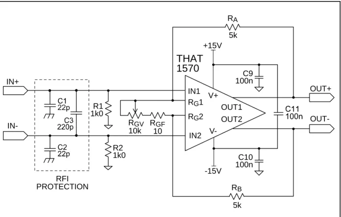
shown in the circuit of Figure 2. In such applications, designers should take care in specify-ing the pot’s element construction to avoid excess noise.
The potentiometer taper will set the circuit’s characteristic of gain vs. pot rotation. Typically, reverse log (audio) taper elements offer the desired behavior in which gain increases with clockwise rotation (and lower values for RGV).
Overall gain accuracy depends on the tolerance of the resistors, including especially the pot (RGV) which dominates RG. Theoretically, when RGV is zero, the gain is determined by RA, RB, RGF alone. End resis-tance (“hop off”) will alter the actual gain; reducing RGF by the amount of end resistance may be appro-priate, especially if the end resistance is consistent. It will be easier to maintain consistent gain at the high-gain end of the pot travel at higher values for RA and RB, since this makes the value of RG required propor-tionately larger for any given gain. The circuit of Figure 2 shows 5 kΩ resistors for RA and RB, so for 60 dB gain, RG = 10 Ω. Its noise performance is very good at 60 dB gain (1.1nV/√Hz, or -133.9 dBu with a zero ohm input termination, or 1.92 nV/√Hz, or -129 dBu with a more realistic 150 Ω input termina-tion). At minimum gain (6 dB) its noise performance is still good (21.3 nV/√Hz), or -108.3 dBu with a zero ohm input termination.
One disadvantage of the circuit of Figure 2 is that differential dc offset at the 1570 output will vary with gain. At 0 dB gain, the 1570’s worst-case differential output offset voltage is ~5 mV, while at 60dB gain, this is ~255 mV. As well, if the wiper of the pot loses contact with the element, gain will abruptly change to unity, with an attendant change in dc offset as well. To minimize dc offsets, consider the circuits of Figures 5 and 7, which ac couple RG.
Improving Noise Performance
The 1570 has extremely low input voltage noise. To achieve this feature, the input transistors are large-geometry NPN types, biased at high (~1 mA) collector current. In order to maintain the low voltage-noise performance of the 1570, designers should take care not to present too high a source impedance to the input pins. A high impedance generates its own self-noise when not shunted by the impedance of the source connected to the input pins.
Additionally, the input transistors’ base current, and any noise in that base current, must be drawn through the bias network (R1 and R2 in Figure 2) connected to IN1 and IN2 (which connect to the bases of the input transistors). Any input current noise will be drawn across the source impedance (as seen by the inputs), which turns it into a voltage that is amplified by the gain of the device. Too high a
+15V
5k
5k
10
10k
V+
V--15V
RFI
PROTECTION
THAT
1570
R
AR
BR
GFR
GVR2
1k0
IN1
IN+
IN-OUT+
OUT-OUT1
OUT2
R
G1
R
G2
IN2
R1
1k0
C9
100n
C10
100n
Figure 2. 1570 Typical Application Circuit Using Single-Gang Pot for Gain Control
Applications
source impedance can easily spoil the noise of the device. The 1kΩ resistors used at R1 and R2 in Figure 2 provide a low source impedance for the 1570 even when the input is open, and provide a 2 kΩ (differential) load for the microphone. Higher source impedances will increase noise seen (and heard!) with open inputs.
One disadvantage of the single-pot approach is that noise at low gains is dominated by the noise of resistors RA and RB. For the circuit of Figure 2, the equivalent input noise at 6 dB gain (the minimum pot setting) is ~21.3 nV/√Hz, or -108.3 dBu. Much lower noise (~ 11.8 nV/√Hz) can be achieved if RA and RB are reduced to ~2.5 kΩ, but to achieve 60 dB gain, this requires RG to be = 5 Ω. (This analysis also assumes RGV = 5 kΩ.)
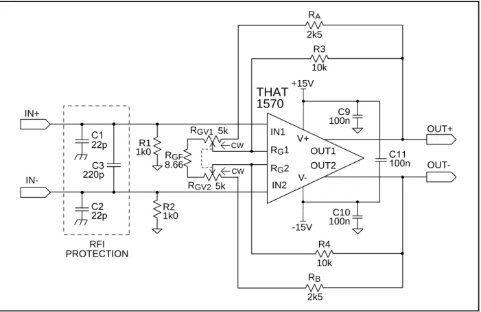
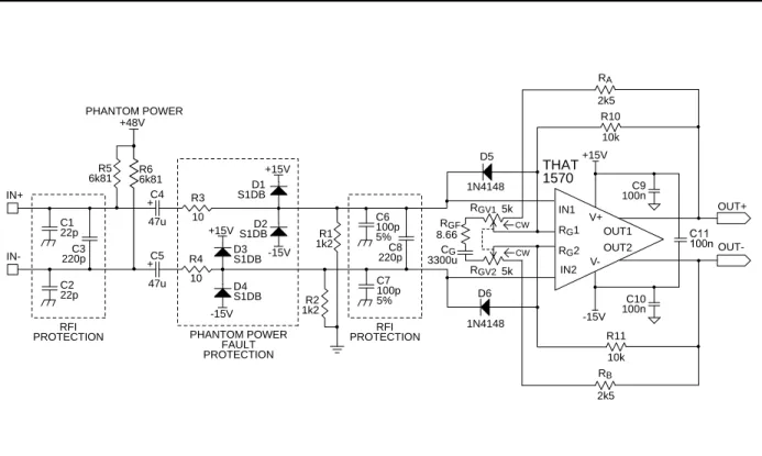
An alternative offered by the 1570 (and not by preamps with internal RA and RB) is that all three resistors may be varied at once. See the circuit of Figure 3, which uses a dual-gang potentiometer as the variable element.
In Figure 3, high gain occurs by decreasing RG while simultaneously increasing RA and RB. The advantage of this approach is that RA and RB will naturally be lower for low gains, without requiring such a low value for RG to achieve high gains. In this circuit, 60 dB gain occurs with RG= 8.66 Ω, and EIN is 1.1 nV/√Hz, or -133.9 dBu with a zero ohm input termination. With a 150 Ω input termination, the
EIN, dominated by the 150 Ω resistor, is 1.92 nV/√Hz or ~ -129 dBu.
This circuit’s minimum gain is 3dB, where RGV is fully CCW. At this gain, the input-referred noise is ~13 nV/√Hz, or -112.5 dBu with a shorted input, and is essentially no different with a 150 Ω input termina-tion. This is about 4.2 dB better than the circuit of Figure 2 at its minimum gain (6dB). Note also that at the minimum +3 dB gain and ±18 V rails, the circuit of Figure 3 can accept up to +25.7 dBu input signals without clipping. This offers more headroom than the circuit of figure 2.
Of course, other minimum and maximum gains can be accommodated by varying the resistors at RA, RB, RGV, and RGF.
For variable-gain applications where gain accuracy is important, THAT recommends using discrete, switched resistors for RA, RB and RG. With switched resistors, it becomes even easier to vary all three resistors to optimize noise.
As with the circuit of Figure 2, RG in Figure 3 is dc coupled. This means that the differential output offset voltage will vary with gain. Also, if the wiper of either half of the gain pot loses contact with the element, gain, and output offset, will change abruptly. R3 and R4 help this situation by minimizing the change in dc offset generated by the 1570’s input bias current (drawn across the combination of R3 in parallel with the series combination of RA and part of
+15V 2k5 2k5 5k 5k V+ V--15V CW CW
THAT
1570
RA 10k R3 RB RGF 8.66 RGV1 RGV2 R2 1k0 IN1 IN+ IN-OUT+ OUT-OUT1 OUT2 RG1 RG2 IN2 R1 1k0 R4 10k RFI PROTECTION C9 100n C10 100nRGV1, or the other mirror half). Again, for best dc performance, consider the circuits of Figures 6 and 8 which ac-couple RG .
Inputs
Simple Configurations
As shown in Figure 4, the 1570 includes protec-tion diodes at all pins except V+ and V-. These diodes reduce the likelihood that accidental electro-static discharge (ESD) or electrical over stress (EOS) will damage the ICs. Other diodes across the base-emitter junctions of the input transistors prevent excessive reverse biasing of these junctions (which would degrade the noise performance of the input devices).
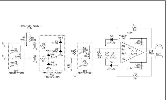
However, while the internal diodes are effective against ESD, they should not be relied upon to protect against excessive input voltage, which can result in significant current flow. This is a particular problem when the preamplifier includes a source of +48 V phantom power (see text below) but can be of concern in any situation where the input may be connected to high signal levels, in which the input signal voltage could exceed the supply rails. The phantom power protection networks shown in Figures 7 and 8 are worth considering even if phantom power is not included in the design.
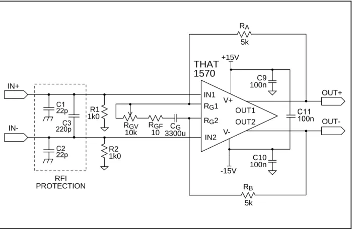
DC Offsets and C
GBecause RG is dc coupled in the circuits of Figure 2 and 3, the differential dc level at the output of the 1570 will vary with gain. In most such applica-tions, the output should be ac-coupled to the next stage, in order to eliminate this varying offset.
For applications where gain is variable, THAT recommends that RG be ac-coupled as shown in Figures 5 and 6. (Figure 5 corresponds to Figure 2, while Figure 6 corresponds to Figure 3.) By adding CG in series with RG, dc gain is fixed at unity. This
+15V
5k
5k
10 3300u
10k
V+
V--15V
RFI
PROTECTION
THAT
1570
R
AR
BR
GFC
GR
GVR2
1k0
IN1
IN+
IN-OUT+
OUT-OUT1
OUT2
R
G1
R
G2
IN2
R1
1k0
C9
100n
C10
100n
Figure 5. 1570 Typical Application Circuit With Single-Gang Pot for Gain Control, AC-Coupled RG
V+ V-IN2 RG2 RG1 IN1 OUT1 3 2 13 7 10 6 15 12 OUT2 -AV -AV
Figure 4. 1570 Equivalent Circuit with Internal Protection Diodes
constrains the differential output dc offset to just over ±5 mV, and prevents it from varying with gain.
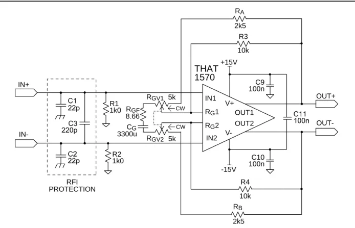
CG must be large enough not to interfere with low-frequency response at the smallest values of RG. With the values shown in Figures 5 and 6, the -3 dB corner is about 5 Hz. Both circuits require a CG of 3,300 μF to maintain this low-frequency corner.
Note also that the voltage appearing across CG is very small. Since polarized electrolytic capacitors normally can withstand some small reverse bias, CG can usually be a polarized capacitor.
Phantom Power
Phantom power is required for many condenser microphones. THAT recommends the circuits of Figure 7 and 8 when phantom power is included. R3, R4, and D1 ~ D6 are used to limit the current that flows through the 1570 inputs when overloaded. These also protect the 1570 when the circuit inputs (IN+ and IN-) are shorted to ground while phantom power is turned on. This causes C4 and/or C5 to dis-charge through other circuit components (including the 1570 inputs), often generating transient currents of several amps. R3 and R4 should be at least 10 Ω to limit destructive currents. (Higher values further limit current flow, but introduce additional source impedance and noise.) Take care to ensure that the resistors used can handle the short-term inrush current; many small surface-mount types cannot. D1
through D4prevent the IC’s inputs from significantly exceeding the supply rails.
D1~D4 prevent the input voltage from exceeding the supply rails. For best results, they should be glass-passivated types (sometimes called “GP”) to ensure low leakage. (Leakage manifests itself as noise in addition to offset.) D5 and D6 steer currents around the input stage in the 1570 further prevent-ing damage.
The series combination of C4 and C5 should be made large to minimize high-pass filtering of the signal based upon the sum of the values of R1+R2. As well, keeping their reactance low relative to the exter-nal microphone's source impedance will avoid increasing the effects of low-frequency current noise in the 1570 input stage.
As in Figures 2 and 3, Figures 7 and 8 differ in their approach to the gain potentiometer. The single-gang pot shown in Figure 7 may be a little less expen-sive to implement, but the dual-gang pot of Figure 8 will deliver better noise performance at low gains, for the reasons noted above. Note that Figure 8 features minimum gain of 3 dB, compared to Figure 7 at 6 dB. The low-frequency corners are about the same (~5 Hz) in the two circuits.
Other manufacturers have recommended, and many pro audio products include, a zener diode arrangement instead of the bridge rectifier to V+ and V- as shown in Figures 7 and 8. THAT does not
Figure 6. 1570 Typical Application Circuit With Dual-Gang Pot for Gain Control, AC-Coupled RG
+15V 2k5 2k5 5k 3300u 5k V+ V--15V CW CW
THAT
1570
RA 10k R3 RB RGF 8.66 CG RGV1 RGV2 R2 1k0 IN1 IN+ IN-OUT+ OUT-OUT1 OUT2 RG1 RG2 IN2 R1 1k0 R4 10k RFI PROTECTION C9 100n C10 100nrecommend the zener approach, because we find that R3 and R4 must be made much larger (e.g., 51 Ω) in order to limit peak currents enough to protect reasonably sized zener diodes (e.g. 1/2 W). Such large series input resistors will limit the noise performance of the preamp. The ultimate floor is set by the impedance of the microphone, but any additional series resistance further degrades performance.
Additionally, while at one time we recommended Schottky diodes for D1~D4 in Figures 7 and 8, we no longer do so. Schottky diodes appeal because of their fast turn-on behavior and low forward voltage drop. However, aside from their higher cost, our experi-ence is that they tend to leak much more than conventional, glass-passivated power diodes, and that their fast turn-on behavior is unnecessary in practice.
For further insights into this subject, see the Audio Engineering Society preprint "The 48 Volt Phantom Menace," by Gary K. Hebert and Frank W. Thomas, presented at the 110th Audio Engineering Society (AES) Convention, and “The Phantom Menace Returns” by Rosalfonso Bortoni and Wayne Kirkwood, presented at the 127th AES Convention.
Outputs
Each of the two 1570 outputs has a dc offset of -610 mV. The differential output has low offset, but this common-mode dc offset must be considered in
connecting the 1570 to subsequent circuitry. Most high-performance A/D converters require a dc offset at their inputs for proper operation. In such cases, drive circuitry should be configured to add the appropriate dc offset to the 1570 outputs in order to match the converter.
As well, the 1570 has common-mode gain of unity, regardless of its differential gain. Common-mode inputs are presented at the output, along with the common-mode dc offset of -610 mV. If these common-mode signals are not removed, they may limit dynamic range of subsequent stages.
If a single-ended output is desired, the THAT1246 is a self-contained differential amplifier which offers a convenient way to remove common mode offset, convert to single-ended, and match the headroom of the 1570 output to a single-ended drive. A dual version of this part, the 1280, and low cost versions (1250 single and 1290 dual) are also avail-able. See Design Note 140, “Input and Output Circuits for THAT Preamplifier ICs” for further ideas. The 1570 will drive loads as low as 2 kΩ, making it possible to drive A/D converters through resistive attenuators in low-cost applications. (However, in order to provide common mode rejection and to improve distortion performance, THAT recommends active designs to drive high-performance A/D convert-ers. In addition to DN140, look for forthcoming application notes that offer more ideas on this subject. THAT 1570 RA RB RGF CG RGV IN1 OUT+ OUT-OUT1 OUT2 RG1 RG2 IN2 +48V RFI
PROTECTION PHANTOM POWER
FAULT PROTECTION PHANTOM POWER R3 10 C4 47u + R4 10 C1 22p C2 22p +15V -15V D1 S1DB D4 S1DB D3 S1DB D2 S1DB +15V -15V R1 1k2 R6 6k81 R5 6k81 R2 1k2 C5 47u + IN+ IN- 220pC3 RFI PROTECTION C6 100p 5% C7 100p 5% C8 220p +15V D5 1N4148 D6 1N4148 V+ V--15V 5k 5k 10 3300u 10k C9 100n C10 100n
CW CW D5 1N4148 D6 1N4148 +48V RFI
PROTECTION PHANTOM POWER
FAULT PROTECTION PHANTOM POWER R3 10 C4 47u + R4 10 C1 22p C2 22p +15V -15V D1 S1DB D4 S1DB D3 S1DB D2 S1DB +15V -15V R1 1k2 R6 6k81 R5 6k81 R2 1k2 C5 47u + IN+ IN- 220pC3 RFI PROTECTION C6 100p 5% C7 100p 5% C8 220p +15V 2k5 2k5 5k 8.66 3300u 5k V+ V--15V THAT 1570 RA 10k R10 RB RGF CG RGV1 RGV2 IN1 OUT+ OUT-OUT1 OUT2 RG1 RG2 IN2 R11 10k C9 100n C10 100n
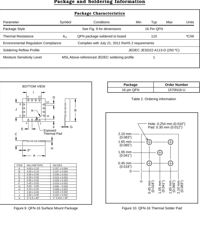
The 1570 QFN package includes a metal thermal pad on its bottom. This pad should be soldered to a thermal pad on the PCB as shown in Figures 9 and 10. Five thermal vias should be arranged in the configuration shown in Figure 10 to provide uniform heat distribution between the top layer of the PCB to the bottom layer. The thermal pad can be left electri-cally floating. However if it is not electrielectri-cally floating, it should be connected only to V-.
For current feedback amplifiers such as the THAT1570, stray capacitance to ground or power planes results in higher gains at high frequencies. This compromises common-mode rejection at high frequencies and, in extreme cases, can even lead to oscillation. Take care to avoid ground and power planes under and near RA, RB, RG, their associated pins and traces.
The input signal lines are susceptible to magnetic pickup from power supply currents, which often take the form of half-wave rectified versions of the signal. Voltage fluctuations on the supply lines can couple capacitively as well. For this reason, take care not to run power and input signal lines close and/or paral-lel to each other.
Minimizing RFI
To minimize RF pickup, the C1 ~ C3 network at the input of all the applications schematics should be located as close as possible to the input connector, and the ground ends of C1 and C2 tied as closely as possible to the chassis. When using the additional RFI protection network C6 ~ C8 (shown in the phantom power circuits Fig. 7 and 8), these compo-nents should be located as close as possible to the 1570’s input pins.
Package and Soldering Information
Parameter Symbol Conditions Min Typ Max Units
Package Style See Fig. 9 for dimensions 16 Pin QFN
Thermal Resistance θJA QFN package soldered to board 110 ºC/W
Environmental Regulation Compliance Complies with July 21, 2011 RoHS 2 requirements
Soldering Reflow Profile JEDEC JESD22-A113-D (250 ºC)
Moisture Sensitivity Level MSL Above-referenced JEDEC soldering profile 1
Package Characteristics A B C D F H I J K Exposed Thermal Pad E G 0°
ITEM MILLIMETERS INCHES A 4.00 ± 0.10 0.157 ± 0.004 B 4.00 ± 0.10 0.157 ± 0.004 C 0.90 ± 0.05 0.035 ± 0.002 D 0.30 ± 0.05 0.012 ± 0.002 E 0.65 ± 0.05 0.026 ± 0.002 F 0.40 ± 0.05 0.016 ± 0.002 G 0.00 ~ 0.05 0.000 ~ 0.020 H 0.20 ± 0.05 0.008 ± 0.002 I 2.60 ± 0.05 0.102 ± 0.002 J 2.60 ± 0.05 0.102 ± 0.002 K C' 0.3 x 45° C‘ 0.012 x 45° 1 4 5 8 9 12 13 16 BOTTOM VIEW
Figure 9. QFN-16 Surface Mount Package
0 0. 45 mm (0.018”) 1. 05 mm (0.041”) 1. 65 mm (0.065”) 2. 10 mm (0.083”) 0 0.45 mm (0.018”) 1.05 mm (0.041”) 1.65 mm (0.065”) 2.10 mm (0.083”) Hole: 0.254 mm (0.010”) Pad: 0.30 mm (0.012”)
Figure 10. QFN-16 Thermal Solder Pad 1570N16-U 16 pin QFN
Order Number Package
Revision History
— Updated bypass capacitor configuration in application
diagrams. Updated Noise specification. 01/12/15
2908 03
1 Added footnote to pin assignment chart.
10/01/13 2827
02
— Corrected typographical errors.
01/05/10 2331 01 — Initial release. 10/06/09 — 00 Page Changes Date ECO Revision