University of Central Florida University of Central Florida
STARS
STARS
Electronic Theses and Dissertations, 2004-2019
2017
Advanced Control Techniques for Efficiency and Power Density
Advanced Control Techniques for Efficiency and Power Density
Improvement of a Three-Phase Microinverter
Improvement of a Three-Phase Microinverter
Seyed Milad Tayebi
University of Central Florida
Part of the Electrical and Computer Engineering Commons
Find similar works at: https://stars.library.ucf.edu/etd University of Central Florida Libraries http://library.ucf.edu
This Doctoral Dissertation (Open Access) is brought to you for free and open access by STARS. It has been accepted for inclusion in Electronic Theses and Dissertations, 2004-2019 by an authorized administrator of STARS. For more information, please contact [email protected].
STARS Citation STARS Citation
Tayebi, Seyed Milad, "Advanced Control Techniques for Efficiency and Power Density Improvement of a Three-Phase Microinverter" (2017). Electronic Theses and Dissertations, 2004-2019. 5934.
ADVANCED CONTROL TECHNIQUES FOR EFFICIENCY AND POWER DENSITY IMPROVEMENT OF A THREE-PHASE MICROINVERTER
by
SEYED MILAD TAYEBI
B.S. Babol University of Technology, 2009 M.S. Iran University of Science and Technology, 2011
A dissertation submitted in partial fulfillment of the requirements for the degree of Doctor of Philosophy
in the Department of Electrical Engineering and Computer Science in the College of Engineering and Computer Science
at the University of Central Florida Orlando, Florida
Summer Term 2017
ii
iii
ABSTRACT
Inverters are widely used in photovoltaic (PV) based power generation systems. Most of these systems have been based on medium to high power string inverters. Microinverters are gaining popularity over their string inverter counterparts in PV based power generation systems due to maximized energy harvesting, high system reliability, modularity, and simple installation. They can be deployed on commercial buildings, residential rooftops, electric poles, etc and have a huge potential market. Emerging trend in power electronics is to increase power density and efficiency while reducing cost. A powerful tool to achieve these objectives is the development of an advanced control system for power electronics.
In low power applications such as solar microinverters, increasing the switching frequency can reduce the size of passive components resulting in higher power density. However, switching losses and electromagnetic interference (EMI) may increase as a consequence of higher switching frequency. Soft switching techniques have been proposed to overcome these issues.
This dissertation presents several innovative control techniques which are used to increase efficiency and power density while reducing cost. Dynamic dead time optimization and dual zone modulation techniques have been proposed in this dissertation to significantly improve the microinverter efficiency. In dynamic dead time optimization technique, pulse width modulation (PWM) dead times are dynamically adjusted as a function of load current to minimize MOSFET body diode conduction time which reduces power dissipation. This control method also improves total harmonic distortion (THD) of the inverter output current. To further improve the microinverter efficiency, a dual-zone modulation has been proposed which introduces one more
iv
soft-switching transition and lower inductor peak current compared to the other boundary conduction mode (BCM) modulation methods.
In addition, an advanced DC link voltage control has been proposed to increase the microinverter power density. This concept minimizes the storage capacitance by allowing greater voltage ripple on the DC link. Therefore, the microinverter reliability can be significantly increased by replacing electrolytic capacitors with film capacitors. These control techniques can be readily implemented on any inverter, motor controller, or switching power amplifier. Since there is no circuit modification involved in implementation of these control techniques and can be easily added to existing controller firmware, it will be very attractive to any potential licensees.
v
To my family
Faeze Mohamadi, Mohsen Tayebi, Shima Tayebi, and Mona Tayebi
vi
ACKNOWLEDGMENTS
I would like to express my sincere appreciation to my advisor, Dr. Issa Batarseh, for his kind support and inspiration to my research work throughout my studies and research at the Florida Power Electronics Center (FPEC). I would also like to thank him for giving me great freedom to pursue independent work.
I would like to thank Dr. Kalpathy B. Sundaram, Dr. Nasser Kutkut, Dr. Wasfy B. Mikhael and Dr. Wei Sun for serving as my committee members, and for their constructive comments and kind suggestions.
I would like to express my deep gratitude to Mr. Charles Jourdan who patiently guided me to the area of the power converters and kindly gave me insightful suggestions throughout my studies and research.
I would also like to thank Dr. Nasser Kutkut and Dr. Haibing Hu for all the advice they have given me to improve my research study.
I would also like to thank the research group at the FPEC, Siddhesh Shinde, Xi Chen, Anirudh Pise, Mahmood Alharbi, Michael Pepper and Christopher Hamilton for their support and intellectual discussions.
At the end, I would like to thank my parents, Faeze Mohamadi and Mohsen Tayebi, for all the love and support they have given me throughout my life. I would also like to thank my sisters, Mona and Shima, for their kind advice and motivations in my life and research work.
vii
TABLE OF CONTENTS
LIST OF FIGURES ... x
LIST OF TABLES ... xv
CHAPTER 1. INTRODUCTION ... 1
1.1 Background and Challenges ... 1
1.2 Microinverter Efficiency Improvement using Dead Time Optimization ... 1
1.3 Boundary Conduction Mode Soft-Switching Techniques ... 5
1.4 DC Link Voltage Control Techniques ... 7
1.5 Research Motivation and Objective ... 11
CHAPTER 2. DYNAMIC DEAD TIME OPTIMIZATION ... 13
2.1 Introduction ... 13
2.2 ZVS Boundary Conduction Mode Current Control of Three-Phase Grid-Tied Inverter 13 2.3 Proposed Dynamic Dead Time Optimization ... 18
2.4 Effects of Circuit Component Nonlinearities ... 20
2.5 Simulation Results... 24
2.6 Advanced Phase Skipping Control ... 25
2.7 Experimental Results... 27
2.8 THD Improvement with Dynamic Dead Time Optimization ... 32
viii
CHAPTER 3. ANALYSIS AND OPTIMIZATION OF VARIABLE-FREQUENCY SOFT-SWITCHING PEAK CURRENT MODE CONTROL TECHNIQUES FOR
MICROINVERTERS ... 35
3.1 Introduction ... 35
3.2 Variable-Frequency Peak Current Mode Control Techniques ... 36
3.3 Power Loss Analysis ... 42
3.4 Proposed Dual-Zone Modulation ... 47
3.5 BCM Peak Current Control ... 55
3.6 Experimental Results... 57
3.7 Summary ... 63
CHAPTER 4. ADVANCED DC LINK VOLTAGE REGULATION AND CAPACITOR MINIMIZATION FOR THREE-PHASE MICROINVERTER ... 64
4.1 Introduction ... 64
4.2 Determining Minimum DC Link Capacitor Value ... 64
4.3 Advanced DC Link Voltage Control ... 77
4.4 Experimental Results... 81
4.5 Summary ... 89
CHAPTER 5. DC LINK VOLTAGE CONTROL WITH PHASE SKIPPING ... 91
ix
5.2 Phase Skipping Control ... 92
5.3 Calculation of Minimum DC Link Capacitor Value with Phase Skipping ... 94
5.3.1 Single-Phase Mode ... 95
5.3.2 Two-Phase Mode ... 97
5.4 Synchronous DC Link Voltage Control with Phase Skipping ... 101
5.5 Experimental Results... 108
5.6 Summary ... 115
CHAPTER 6. CONCLUSIONS AND FUTURE WORK ... 117
6.1 Conclusion ... 117
6.2 Future Works ... 118
x
LIST OF FIGURES
Figure 1-1: Single-phase half-bridge inverter with the corresponding controller. ... 2
Figure 1-2: Three ZVS BCM modulation methods: (a) fixed reverse current, (b) variable reverse current, (c) fixed band width. ... 6
Figure 1-3: Two-stage microinverter topology. ... 7
Figure 1-4: Typical DC link voltage control system. ... 8
Figure 1-5: DC link voltage control using a digital finite impulse response (FIR) filter [36]. ... 9
Figure 1-6: Control method proposed by Brekken et al. [37]. ... 10
Figure 1-7: Voltage ripple estimation method proposed by Ninad and Lopes [38]. ... 10
Figure 2-1: Three-phase half-bridge inverter. ... 14
Figure 2-2: Operating intervals of a single-phase half-bridge inverter. ... 15
Figure 2-3: Inductor current and driving signals for BCM ZVS current control... 16
Figure 2-4: Upper and lower boundaries for BCM ZVS current control with fixed reverse current. ... 17
Figure 2-5: ZVS dead time resonant intervals: (a) turn-on dead time interval (td1), (b) turn-off dead time interval (td2). ... 19
Figure 2-6: Coss versus Drain Source voltage for Fairchild FCB20N60F MOSFET. ... 21
Figure 2-7: Inductance versus DC current for a gapped ferrite inductor. ... 22
Figure 2-8: Z0 versus dead time at full load (Peak current). ... 22
Figure 2-9: Optimum dead time versus fixed dead time at full load. ... 23
Figure 2-10: Inductor current with BCM current control and fixed reverse current. ... 24
xi
Figure 2-12: Dead times with Dynamic Dead Time Optimization. ... 25
Figure 2-13: Filter inductor current. ... 28
Figure 2-14: Experimental waveforms with fixed dead time. ... 28
Figure 2-15: Experimental waveforms with Dynamic Dead Time Optimization... 29
Figure 2-16: Micro-inverter output stage efficiency with FCB20N60F MOSFET. ... 29
Figure 2-17: Micro-inverter output stage efficiency with STB21N65M5 MOSFET. ... 30
Figure 2-18: Output current and inductor current with fixed dead time. ... 32
Figure 2-19: Output current and inductor current with dynamic dead time optimization. ... 33
Figure 3-1: Three-phase half-bridge inverter. ... 36
Figure 3-2: Three different ZVS BCM modulation methods: (a) fixed reverse current, (b) variable reverse current, (c) fixed band width. ... 37
Figure 3-3: Switching frequency over a half 60-Hz line cycle with varying Io for: (a) fixed reverse current, (b) variable reverse current, and (c) fixed band width. ... 40
Figure 3-4: Inductor rms current versus Io for each modulation method at full load. ... 41
Figure 3-5: Optimum peak current boundaries for three modulation methods at various power levels. ... 46
Figure 3-6: Dual-zone modulation method. ... 47
Figure 3-7: Dual-zone modulation method switching waveforms: (a) Zone 1, (b) Zone 2. ... 49
Figure 3-8: Optimum peak current boundaries for dual-zone modulation method at (a) 100%, (b) 30% of rated power. ... 51
xii
Figure 3-10: Dual-zone modulation switching frequency range for 100% and 30% of rated
power... 53
Figure 3-11: Power loss distribution with different BCM modulation methods at 100%, 50% and 30% of microinverter rated power. ... 54
Figure 3-12: DSP implementation of BCM peak current control. ... 56
Figure 3-13: Filter inductor current and output current for (a) BCM with fixed reverse current, (b) BCM with variable reverse current, (c) BCM with fixed bandwidth. ... 58
Figure 3-14: Optimum peak current boundaries for three modulation methods at various power levels. ... 59
Figure 3-15: Dual-zone peak current modulation at (a) high power, (b) low power. ... 60
Figure 3-16: Dual-zone modulation method switching waveforms: (a) Zone 1, (b) Zone 2. ... 61
Figure 3-17: Microinverter output stage efficiency with different modulation methods. ... 62
Figure 4-1: Two-stage microinverter topology. ... 65
Figure 4-2: Three-phase half-bridge microinverter with a bipolar DC link. ... 68
Figure 4-3: Simulation results of single-phase operation. ... 69
Figure 4-4: Key waveforms of the microinverter. ... 71
Figure 4-5: Bipolar DC link voltage ripple with different storage capacitance in a balanced system. ... 76
Figure 4-6: Bipolar DC link voltage ripple with different storage capacitance in an unbalanced system. ... 76
Figure 4-7: Typical DC link voltage control system. ... 78
xiii
Figure 4-9: PLL-based DC link voltage control dynamic model. ... 81
Figure 4-10: Two-stage three-phase microinverter prototype topology. ... 82
Figure 4-11: Microinverter DC link voltage and three-phase output voltage with (a) 40 µF and (b) 8 µF DC link capacitors. ... 84
Figure 4-12: Three-phase inverter output current and DC link voltage in (a) an unstable and (b) a stable system. ... 86
Figure 4-13: Dynamic response to the step change in the input power from 260 W to 375 W along with an expanded view. ... 87
Figure 4-14: Dynamic response to the step change in the input power from 375 W to 260 W along with an expanded view. ... 88
Figure 5-1: Three-phase micro-inverter operating modes. ... 93
Figure 5-2: Three-phase half-bridge microinverter with a bipolar DC link. ... 94
Figure 5-3: Key waveforms of the microinverter in single-phase mode. ... 96
Figure 5-4: Key waveforms of the microinverter in two-phase mode. ... 98
Figure 5-5: Bipolar DC link voltage ripple with different storage capacitance in two-phase mode. ... 101
Figure 5-6: Typical DC link voltage control system. ... 103
Figure 5-7: Proposed PLL-synchronized DC link voltage control system with phase skipping control. ... 105
Figure 5-8: Proposed PLL-synchronized DC link voltage sampling time in the single-phase mode. ... 105
xiv
Figure 5-10: Proposed controller response to a ramp change in input PV power. ... 107 Figure 5-11: Two-stage three-phase microinverter prototype topology. ... 109 Figure 5-12: Microinverter DC link voltage and output voltage in (a) three-phase mode, (b) two-phase mode, and (c) single-two-phase mode. ... 110 Figure 5-13: Dynamic response to the step change in the input power. ... 111 Figure 5-14: Inverter output current and its harmonic spectrum with, (a) the proposed DC link voltage control, (b) a high-frequency DC link voltage control. ... 112 Figure 5-15: Control error signal with, (a) a high-frequency DC link voltage control
(THD=3.8%), (b) the proposed DC link voltage control (THD=1.6%). ... 113 Figure 5-16: Controller performance when PV power changes from 220 W to 150 W. ... 115
xv
LIST OF TABLES
Table 2-1: Two Different Manufacturer’s MOSFETs Specifications ... 28
Table 2-2: CEC Weighted Efficiency for Different Modes of Operation ... 31
Table 3-1: Inverter Prototype Operating Parameters ... 43
Table 3-2: THD and Inductor RMS Current for Four Current Modulation Methods ... 62
1
CHAPTER 1.
INTRODUCTION
1.1 Background and Challenges
Among renewable energy sources, solar energy has gained considerable attention in recent years [1], [2]. In order to convert this source of energy into electricity and inject it into the utility grid, power converters with high efficiency and power density need to be developed. There are three basic architectures for photovoltaic (PV) solar systems; centralized inverter, string inverter and microinverter. PV microinverter architecture is the fastest growing technology due to its advantages such as enhanced energy harvesting, high reliability, and simple installation. Microinverters with typical power levels from 200 W to 400 W can be directly mounted on the back of the PV panels.
Emerging trend in power electronics is to increase power density and efficiency of the microinverters while reducing cost. Employing high switching frequency and soft switching techniques reduce cost by reducing the size of passive components and improve efficiency by decreasing switching losses. Soft switching can be improved by minimizing MOSFET body diode conduction time. In order to achieve high power conversion efficiency and power density, a comprehensive investigation and research have been conducted on new topologies and control techniques.
1.2 Microinverter Efficiency Improvement using Dead Time Optimization
Figure 1-1 depicts a single-phase half-bridge inverter with a controller providing duty cycles and dead times for the MOSFETs. The inverter MOSFET gates are driven by alternating PWM signals
2
so that when one MOSFET is on, the other is off. Dead time is the state where both MOSFETs are off and one MOSFET’s body diode is conducting. Since body diode conduction losses are higher than MOSFET conduction losses, efficiency is maximized when body diode conduction time is small. Body diode conduction time is directly proportional to dead time, therefore it is advantageous to select a dead time value that minimizes body diode conduction time without resulting in shoot-through current.
Figure 1-1: Single-phase half-bridge inverter with the corresponding controller.
Excessive dead time can also have a negative impact on inverter efficiency especially at higher operating frequencies where it is a large percentage of the conduction time.
Typically, a fixed dead time is determined based on the worst-case operating conditions such as load, voltage and temperature variations. The body diode conduction loss can be approximated as follows:
3
where, VDS is drain to source voltage or the diode forward voltage drop, IL is inductor current during the dead times, td1 and td2 are turn-on and turn-off dead times, respectively and fsw is switching frequency. Referring to equation (1-1), it can be seen that excessive dead time increases the body diode conduction loss due to the diode’s forward voltage drop.
A number of research papers on PWM dead time optimization for various buck derived topologies have been published [3]-[13].
Switching current sensing was proposed in [3] for buck converters to measure the current flowing through the synchronous MOSFET and detect shoot-through current. When shoot-through occurs, the dead times must be increased. However, this method requires high bandwidth sensors for current measurement which makes its implementation difficult and adds cost.
Switching voltage sensing is sub-divided into the adaptive [4]-[6] and predictive [7]-[9] types. Adaptive control measures the switching voltage across the synchronous rectifier and adjusts the dead times accordingly. Predictive control uses the information from the previous switching cycle to adjust the dead times in the current cycle. Although the experimental results show a significant reduction in body diode losses, these control methods require additional circuit components which drive cost up and decrease reliability. Therefore, sensorless optimization methods have been proposed that do not require additional components.
Sensorless dead time optimization for dc-dc converters was proposed in [10] based on maximum power point tracking (MPPT). This method optimizes the dead time by indirectly measuring the efficiency of the converter. Another sensorless dead time optimization method proposed in [11] optimizes the efficiency by minimizing the duty cycle in dc-dc converters. This method is able to
4
optimize both turn-on and turn-off dead times. A perturb and observe algorithm (P&O) was proposed in [12] to detect dead time resulting in maximum efficiency.
Several methods have been proposed to overcome the dead time issues in inverters. A correlation-based control technique was introduced in [13] to optimize dead time in motor drive inverters. The algorithm dynamically minimizes the input current resulting in minimum power loss. The technique proposed in [14] compensates for the effect of dead time by adjusting the switching frequency in sinusoidal pulse-width-modulated voltage-source inverters. Another dead time compensation method was presented in [15] based on harmonic analysis and filtering of the voltage distortion produced by dead time effects by adding a predetermined compensation signal to the voltage reference in ac motor drives. However, this method requires extra components which increases the cost and circuit complexity.
The method introduced in [16] improves THD and the magnitude of the inverter output voltage by preventing the unnecessary dead time. Another switching strategy for PWM power converters was proposed in [17] on the basis of using independent on/off switching action according to the current polarity. As long as the current polarity does not change, the dead time is not needed. These methods can be affected by detection circuit delay, harmonics and A/D converter errors.
A dynamic dead time optimization technique is proposed and will be discussed in the next chapter of this dissertation wherein the PWM dead times are calculated by sensing the grid voltage which is also used for duty cycle calculation.
5
1.3 Boundary Conduction Mode Soft-Switching Techniques
In most soft-switching techniques, resonant circuits or auxiliary components are used to achieve zero voltage switching (ZVS) or zero current switching (ZCS). These additional auxiliary components and switches will reduce reliability and add cost to the inverter design. These techniques can be basically classified into dc-side and ac-side topologies.
In dc-side topologies, the auxiliary circuits are placed between the input dc power supply and main bridges. One-switch clamped resonant DC link [18], passive clamped using the couple inductors [19], and one-switch resonant inverter [20], [21] have been proposed to achieve soft switching. However, these topologies suffer from voltage stress and reliability issues. Parallel resonant DC link techniques have been proposed in [22], [23] which require large active component count. AC-side topologies are used for high-power applications where the auxiliary circuits are placed on the ac side of the main power bridge. These techniques are classified into zero-voltage transition (ZVT) and zero-current transition (ZCT). Topologies such as ZVT inverter with coupled inductor feedback [24], [25] and three auxiliary switches [26], [27] have been proposed in this category. However, they are not suitable for practical implementation due to their circuit and control complexity. ZCT topologies are typically used in high-power inverters where diode reverse recovery and turn-off losses are dominant. ZCT inverter topologies with three [28] and six [29]-[31] auxiliary switches have been introduced which maintain low voltage stress across diodes and switches. However, cost, control and circuit complexity are the main disadvantages.
The above mentioned soft-switching techniques require additional components and auxiliary devices which reduce reliability and add cost and control complexity to the inverter design.
6
To solve these issues, several boundary conduction mode (BCM) modulation methods have been proposed that can achieve soft switching without the need for additional components or analog circuits.
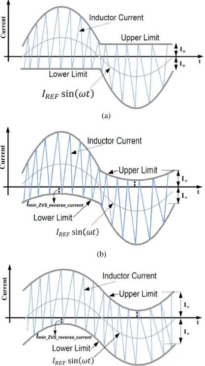
ZVS BCM peak current control is a promising soft switching candidate for low power applications where the switching losses are usually dominant [32]-[34]. For this purpose, three different peak current mode control methods have been introduced in [35]: BCM with fixed reverse current, BCM with variable reverse current, and BCM with fixed bandwidth. In these modulation methods, the inductor current is bidirectional during switching cycle to achieve turn-on ZVS. Although BCM control results in increased rms current, conduction losses and core losses when compared to continuous-conduction mode (CCM), switching losses are greatly reduced.
Figure 1-2 shows these three BCM modulation methods where the inductor current is reversed during each switching cycle to achieve turn-on ZVS for each switch.
(a) (b) (c)
Figure 1-2: Three ZVS BCM modulation methods: (a) fixed reverse current, (b) variable reverse current, (c) fixed band width.
In order to further improve efficiency, a new BCM modulation technique is proposed in this dissertation that introduces one more soft-switching transition and lower inductor peak current compared to the three mentioned BCM modulation methods.
7
1.4 DC Link Voltage Control Techniques
Figure 1-3 shows a common two-stage microinverter topology. This topology which connects the PV panel to the grid consists of a DC/DC converter and a DC/AC inverter along with a decoupling (DC link) capacitor in between the two stages. Typically, the first stage provides a maximum power point tracking (MPPT) function for the PV panel and boosts its low voltage to a constant DC link voltage.
Figure 1-3: Two-stage microinverter topology.
Figure 1-4 shows a typical DC link voltage control system. In a two-stage microinverter, the DC link voltage control continually senses the DC link voltage and compares it with an average voltage reference so that the compensator loop regulates the inverter output current accordingly. Presence of large voltage ripple on the DC link capacitor introduces large ripples in the DC link voltage sense path to the controller and consequently in the inverter output current if it is not filtered by the DC link voltage control loop. There exists two approaches in order to mitigate this effect: 1) Large values of DC link capacitors are often employed to attenuate DC link voltage ripple. This requires the use of electrolytic capacitors that suffer from limited lifetime and poor reliability, or
8
high value polypropylene film capacitors that are expensive and bulky which reduces power density and increases cost. 2) An alternative method is to use analog or digital filters to attenuate harmonic distortion in the inverter output current caused by the DC link voltage ripple. In the case of high peak-to-peak voltage ripple on the DC link, an analog filter requires a very high attenuation at low frequencies which results in lower loop bandwidth. Therefore, an analog low-pass filter placed in the DC link voltage sense path will exhibit poor transient response as well as adding cost to the design. Digital low-pass filters of varying complexity have also been proposed in order to mitigate the harmonic content in the error signal [36]-[39]. These filters provide some improvement but increase complexity and computation time, and are unable to eliminate all of the harmonic content.
Figure 1-4: Typical DC link voltage control system.
Various DC link voltage control techniques have been proposed to mitigate the effect of DC link voltage ripple. Figure 1-5 shows the DC link voltage control using a digital finite impulse response (FIR) filter proposed in [36]. A digital FIR filter is used in [36] to sample the DC link voltage at a
9
low-frequency rate and then calculate the average voltage in order to reduce output current harmonics. However, the controller response to even small power transients is quite slow.
Figure 1-5: DC link voltage control using a digital finite impulse response (FIR) filter [36].
Figure 1-6 shows another technique to reduce the effect of DC link voltage ripple on the inverter output current [37]. This technique uses a digital current regulator to filter harmonics caused by the DC link voltage ripple. However, the voltage loop cutoff frequency is low which degrades the system dynamic performance.
10
Figure 1-6: Control method proposed by Brekken et al. [37].
Figure 1-7 shows voltage ripple estimation method proposed by Ninad and Lopes[38]. In an effort to mitigate the effect of DC link voltage ripple on the inverter output current, voltage ripple is estimated to be added to the DC link reference voltage. The result will then be compared with the measured DC link voltage to be fed to the loop compensator. Another predictive control method was proposed in [39] based on power balance and the relationship between energy and DC capacitor voltage to filter the DC link voltage ripple. In these techniques [38], [39], accuracy and computation time will suffer.
11
A coupled inductor filter is presented in [40] to eliminate a specific frequency from the output of a DC/DC converter which adds ciricuit component and cost to the design. A control loop compensator is proposed in [41] and [42] to minimize the output harmonics using a high-order filter with low-frequency poles and zeros which increases complexity and computation time. A third ripple port in a single-phase inverter is presented in [43] to cancel the DC link voltage ripple using a small capacitor which requires additional circuit components.
In this dissertation, a PLL-synchronized DC link voltage control is proposed to tightly regulate the DC link voltage regardless of large voltage ripple without the need for analog or digital filters.
1.5 Research Motivation and Objective
The objective of this dissertation is to improve the microinverter efficiency and power density by developing advanced control techniques without the need for additional components and analog circuits. Therefore, the development targets can be summarized as follows:
• To employ dead time optimization without any additional circuit components
• To implement soft switching technique in digital controller firmware
• To achieve more than 96% efficiency in the inverter stage
• To increase the microinverter system’s lifespan to more than 20 years
• To increase the microinverter power density more than 12 W/in3
With this in mind, the research objectives of this dissertation are summarized as follows:
• To develop a dynamic dead time optimization technique and implement it in the inverter
12
• To improve total harmonic distortion of the inverter output current caused by dead time
• To optimize the boundaries of BCM modulation methods and develop a new soft-switching
modulation technique for further efficiency improvement
• To develop a new DC link voltage control that allows higher voltage ripple and increases
power density
• To increase the microinverter reliability by replacing electrolytic capacitors with film
13
CHAPTER 2.
DYNAMIC DEAD TIME OPTIMIZATION
2.1 Introduction
This chapter introduces two efficiency improvement techniques for a grid-tied micro-inverter with current mode control zero voltage switching (ZVS) output stages. The first technique is dynamic dead time optimization wherein PWM dead times are dynamically adjusted as a function of load current. The second method is advanced phase-skipping control which maximizes inverter efficiency by controlling power on individual phases depending on the available input power from the PV source. Neither of the techniques require any additional circuit components and both can be easily implemented in digital controller firmware. The two techniques were designed and implemented in a 400W three-phase micro-inverter prototype and the experimental results validate the theoretical analysis of these techniques and demonstrate that a significant efficiency improvement can be achieved.
2.2 ZVS Boundary Conduction Mode Current Control of Three-Phase Grid-Tied Inverter
Figure 2-1 depicts a standard three-phase half-bridge grid-tied inverter. MOSFET body diodes and parasitic capacitors play an important role when implementing ZVS in an inverter output stage. In order to achieve ZVS, the bidirectional current flow discharges the MOSFET parasitic capacitor and then the body diode conducts prior to each switching transition to apply zero voltage across the MOSFET.
Although the three phases operate independently, it can be assumed that the system is balanced. Therefore, the analysis can be performed on one of the three phases. In order to simplify the
14
analysis of the inverter stage, steady state operation is assumed with the output voltage equal to the grid voltage. The output voltage is considered to be constant during one switching period of the output stage due to the large difference between the inverter switching frequency and the grid frequency.
Figure 2-1: Three-phase half-bridge inverter.
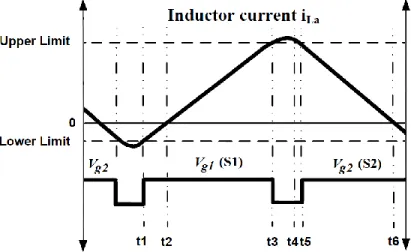
Interval 1 (t1-t3): In this interval, as shown in Figures 2-2 and 2-3, the upper switch (S1) is on while
the lower switch (S2) is off. Since voltage across the inductor is positive, the inductor current is linearly increasing. The inductor current can be calculated as follows:
𝑖𝐿(𝑡) =𝑉𝑑𝑐⁄ −𝑉2 𝑎𝑐
𝐿 𝑡 + 𝑖𝐿(𝑡1) ( 2-1 )
Interval 2 (t3-t4): In this interval, the inductor current reaches the upper limit and then the upper
switch (S1) is turned off. As shown in Figure 2-2, both switches are off and the parasitic capacitors of the MOSFETs S1 and S2 are being respectively charged and discharged by the inductor current. This interval is the resonant interval, and the inductor current and parasitic capacitors voltage can be calculated as follows:
15 { 𝑖𝐿(𝑡) = 𝑉𝑑𝑐⁄ −𝑉2 𝑎𝑐 𝑍𝑜 𝑠𝑖𝑛𝜔𝑜(𝑡 − 𝑡3) + 𝑖𝐿(𝑡3)𝑐𝑜𝑠𝜔𝑜(𝑡 − 𝑡3) 1 𝑉𝐶𝑆1(𝑡) = (𝑉𝑑𝑐⁄ − 𝑉2 𝑎𝑐) + 𝑖𝐿(𝑡3)𝑍𝑜𝑠𝑖𝑛𝜔𝑜(𝑡 − 𝑡3) −(𝑉𝑑𝑐⁄ − 𝑉2 𝑎𝑐)𝑐𝑜𝑠𝜔𝑜(𝑡 − 𝑡3) 1 𝑉𝐶𝑆2(𝑡) = (𝑉𝑑𝑐⁄ + 𝑉2 𝑎𝑐) − 𝑖𝐿(𝑡3)𝑍𝑜𝑠𝑖𝑛𝜔𝑜(𝑡 − 𝑡3) +(𝑉𝑑𝑐⁄ − 𝑉2 𝑎𝑐)𝑐𝑜𝑠𝜔𝑜(𝑡 − 𝑡3) ( 2-2 )
where, ωo, the natural resonant frequency, and Zo, the characteristic impedance of the resonant tank are respectively defined as follows:
{ 𝜔0 = 1 √𝐿. 2𝐶 ⁄ 𝑍0 = √𝐿 2𝐶⁄ 𝐶𝑠1= 𝐶𝑠2= 𝐶 ( 2-3 )
Figure 2-2: Operating intervals of a single-phase half-bridge inverter.
16
Figure 2-3: Inductor current and driving signals for BCM ZVS current control.
Interval 3 (t4-t6): In this interval, as soon as the parasitic capacitors of the MOSFETs S1 and S2 are
fully charged and discharged respectively and the voltage on C2 is zero, the body diode of MOSFET S2 (D2) starts conducting at t4. Therefore, zero voltage is applied across MOSFET S2 and it is ready to be turned on under ZVS condition. At t5, the lower switch (S2) turns on and the inductor current flowing through the body diode is transferred to the switch (S2).
During this interval, since voltage across the inductor is negative, the inductor current is linearly decreasing and can be approximated as follows:
𝑖𝐿(𝑡) =−𝑉𝑑𝑐⁄ −𝑉2 𝑎𝑐
𝐿 𝑡 + 𝑖𝐿(𝑡4) ( 2-4 ) For ZVS boundary conduction mode (BCM) control implementation, the upper and lower boundaries of the inductor current need to be determined so that the inverter injects only AC current to the grid. Therefore, the average output current must be equal to the reference current during each switching cycle.
There are three possible inductor current modulation methods satisfying this requirement: BCM with fixed reverse current, BCM with variable reverse current, and BCM with fixed bandwidth.
17
Figure 2-4 depicts the upper and lower boundaries of BCM with fixed reverse current modulation along with the average inductor current. For the positive half cycle, the upper boundary is determined so that the average current is equal to the reference current during each switching cycle, while the lower boundary provides the reverse current to discharge the MOSFET parasitic capacitors in order to achieve ZVS during each switching period.
Figure 2-4: Upper and lower boundaries for BCM ZVS current control with fixed reverse current.
Similarly, for the negative half cycle, the upper limit provides ZVS for the MOSFETs and the lower limit produces the reference current. It can be seen that the average current is equal to the reference current. The upper and lower boundaries for this inductor current modulation can be calculated as follows: {𝐼𝑢𝑝𝑝𝑒𝑟 = 2𝐼𝑅𝐸𝐹sin(𝜔𝑡) + 𝐼𝑜 𝐼𝑙𝑜𝑤𝑒𝑟 = −𝐼𝑜 , if sin (𝜔𝑡) ≥ 0 ( 2-5 ) {𝐼𝑢𝑝𝑝𝑒𝑟 = 𝐼𝑜 𝐼𝑙𝑜𝑤𝑒𝑟 = 2𝐼𝑅𝐸𝐹sin(𝜔𝑡) − 𝐼𝑜 , if sin (𝜔𝑡) < 0
18
where, Io is the reverse current for achieving ZVS and IREF is the reference peak current. It should be noted that IREF is a function of the available input power and Io selection criteria are addressed in [44].
Referring to Figure 2-4, during the time where the inductor current transitions from positive to negative on positive half cycles and from negative to positive on negative half cycles, ZVS is realized. The power dissipation during this interval is a function of the amount of time that the ZVS MOSFET’s body diode is conducting. This time is determined by the amount of fixed dead time provided by the controller.
With fixed dead time control, a constant value of dead time is applied for both on and turn-off transitions throughout the entire grid cycle. The dead times must be long enough to achieve ZVS by allowing the inductor current to fully charge and discharge the MOSFET parasitic capacitors. The required dead time can be calculated as follows:
𝑡𝑑 = 2𝐶𝑉𝑑𝑐
𝐼𝑜 ( 2-6 )
where, C is the MOSFET parasitic capacitors, Vdc is the voltage on the MOSFET parasitic capacitors and Io is the minimum worst-case reverse inductor current.
2.3 Proposed Dynamic Dead Time Optimization
The dead time interval consists of the resonant interval and the body diode conduction time. Dynamic Dead Time Optimization minimizes the MOSFET’s body diode conduction time during the dead time interval [45]. The resonant intervals (t3-t4) and (t7-t8) are shown in Figure 2-5(a) and (b), respectively. During the first resonant interval (t3-t4), turn-on dead time, the MOSFETs parasitic capacitance voltage can be calculated as follows:
19 { 𝑉𝐶𝑆1(𝑡) = (𝑉𝑑𝑐⁄ − 𝑉2 𝑎𝑐) − (𝑉𝑑𝑐⁄ − 𝑉2 𝑎𝑐)𝑐𝑜𝑠𝜔𝑜(𝑡 − 𝑡3) +𝑍𝑜. 𝐼𝑢𝑝𝑝𝑒𝑟𝑠𝑖𝑛𝜔𝑜(𝑡 − 𝑡3) 𝑉𝐶𝑆2(𝑡) = (𝑉𝑑𝑐⁄ + 𝑉2 𝑎𝑐) + (𝑉𝑑𝑐⁄ − 𝑉2 𝑎𝑐)𝑐𝑜𝑠𝜔𝑜(𝑡 − 𝑡3) −𝑍𝑜. 𝐼𝑢𝑝𝑝𝑒𝑟𝑠𝑖𝑛𝜔𝑜(𝑡 − 𝑡3) ( 2-7 ) (a) (b)
Figure 2-5: ZVS dead time resonant intervals: (a) turn-on dead time interval (td1), (b) turn-off dead time interval (td2).
Similarly, during the second resonant interval (t7-t8), turn-off dead time, the MOSFETs parasitic capacitance voltage can be determined as follows:
{ 𝑉𝐶𝑆1(𝑡) = (𝑉𝑑𝑐⁄ − 𝑉2 𝑎𝑐) + (𝑉𝑑𝑐⁄ + 𝑉2 𝑎𝑐)𝑐𝑜𝑠𝜔𝑜(𝑡 − 𝑡7) +𝑍𝑜. 𝐼𝑙𝑜𝑤𝑒𝑟𝑠𝑖𝑛𝜔𝑜(𝑡 − 𝑡7) 𝑉𝐶𝑆2(𝑡) = (𝑉𝑑𝑐⁄ + 𝑉2 𝑎𝑐) − (𝑉𝑑𝑐⁄ + 𝑉2 𝑎𝑐)𝑐𝑜𝑠𝜔𝑜(𝑡 − 𝑡7) −𝑍𝑜. 𝐼𝑙𝑜𝑤𝑒𝑟𝑠𝑖𝑛𝜔𝑜(𝑡 − 𝑡7) ( 2-8 )
20
Referring to Figure 2-5, if the voltage at the switch node ‘a’ is known, the voltage on the MOSFET parasitic capacitors can be determined. The switch node voltage 𝑉𝑎𝑁(𝑡) during dead time is given by
𝑉𝑎𝑁(𝑡) = 𝑉𝑑𝑐⁄ − 𝑉2 𝐶𝑆1(𝑡) = 𝑉𝐶𝑆2(𝑡) − 𝑉𝑑𝑐⁄2 ( 2-9 ) Using equations (2-7), (2-8) and (2-9), the switch node voltages, 𝑉𝑎𝑁1(𝑡) and 𝑉𝑎𝑁2(𝑡), during the turn-on dead time (td1) and turn-off dead time (td2) can be calculated as follows, respectively:
𝑉𝑎𝑁1(𝑡) = 𝑉𝑎𝑐 + (𝑉𝑑𝑐
2 − 𝑉𝑎𝑐) 𝑐𝑜𝑠𝜔𝑜(𝑡𝑑1) − 𝑍𝑜. 𝐼𝑢𝑝𝑝𝑒𝑟𝑠𝑖𝑛𝜔𝑜(𝑡𝑑1) ( 2-10 ) 𝑉𝑎𝑁2(𝑡) = 𝑉𝑎𝑐− (
𝑉𝑑𝑐
2 + 𝑉𝑎𝑐) 𝑐𝑜𝑠𝜔𝑜(𝑡𝑑2) − 𝑍𝑜. 𝐼𝑙𝑜𝑤𝑒𝑟𝑠𝑖𝑛𝜔𝑜(𝑡𝑑2) ( 2-11 ) where, td1and td2 are t4-t3 and t8-t7, respectively.
2.4 Effects of Circuit Component Nonlinearities
Device parasitic capacitances are inherent due to semiconductor physics and have a nonlinear nature. These nonlinear capacitances have a negative impact on switching transition times and therefore on switching loss.A nonlinear capacitor can be modeled by a linear equivalent [46], [47] or circuit simulators [48], [49].
During each resonant interval, the MOSFET parasitic capacitance voltage (VCS) transitions from 0 V to Vdc or vice versa depending on the switching edge. For example, in Figure 2-5(a), the upper MOSFET’s parasitic capacitor voltage (VCS1(t)) transitions from 0 V to Vdc, while VCS2(t) transitions from Vdc to 0 V. VCS1(t) and VCS2(t) are defined by equation (2-7). During these transition times, the MOSFET parasitic capacitance varies with the value of VCS1(t) and VCS2(t). This capacitance can be expressed as
21
Therefore, the definition from (2-3) can be rewritten as follows:
{ 𝜔0 = 1 √𝐿. 2𝐶𝑂𝑆𝑆(𝑉𝑑𝑠) ⁄ 𝑍0 = √𝐿 2𝐶 𝑂𝑆𝑆(𝑉𝑑𝑠) ⁄ 𝐶𝑠1= 𝐶𝑠2= 𝐶𝑂𝑆𝑆(𝑉𝑑𝑠) ( 2-13 )
Figure 2-6 demonstrates the variation in COSS for a Fairchild FCB20N60F MOSFET extracted from the device datasheet and fitted to a curve using discrete data points. Referring to the figure, the value of the capacitance drastically drops when Vds increases from 0 V to 50 V, whereas it has a relatively constant value for voltages greater than 50 V.
The nonlinear nature of the MOSFET output capacitance has been taken into account in computing optimum dead times in equations (2-10) and (2-11). In both simulated and experimental results, the DC link voltage was set at 400 V. Therefore, the nonlinear voltage dependent capacitance must be charged and discharged from 0 V to 400 V.
Figure 2-6: Coss versus Drain Source voltage for Fairchild FCB20N60F MOSFET.
Virtually all inductors used in power filter circuits exhibit a decrease in inductance with increasing current. This inductance decrease is often nonlinear and varies with core material and magnetic
22
circuit structure. Figure 2-7 shows the inductance versus DC current for a 270 µH, 4 A gapped ferrite inductor.
Figure 2-7: Inductance versus DC current for a gapped ferrite inductor.
Figure 2-8 shows Zo versus dead time at peak current and full load with both fixed and variable inductance values. It can be seen in the figure that a varying inductance value has a minimal effect on the value of Zo and consequently from equations (2-10) and (2-11) an insignificant effect on dead time when compared to the effect of the nonlinear parasitic capacitance of a MOSFET.
23
Optimum dead time is calculated for each switching cycle iteratively as opposed to fixed dead time where one dead time value would be selected for all operating points. Equations (2-10) and (2-11) were implemented in MATLAB. td1 and td2 were incremented in one nano second steps to yield a range of optimum dead time values for switch node voltages between +200 V and -200 V for each switching cycle. Figure 2-9 shows optimum dead times calculated using equations 10) and (2-11) during positive and negative half cycles for the 400-W three-phase micro-inverter prototype operating at full load, given the fact that 𝑉𝑎𝑁1(𝑡) transitions from 𝑉𝑑𝑐⁄2 to −𝑉𝑑𝑐⁄2 and 𝑉𝑎𝑁2(𝑡) transitions from −𝑉𝑑𝑐⁄2 to 𝑉𝑑𝑐⁄2. The fixed dead time for this prototype was set at 530 ns for both turn-on and turn-off transitions. The MOSFETs used are Fairchild FCB20N60F with Vdc=400
V and a 270 µH gapped ferrite output filter inductor.
Figure 2-9: Optimum dead time versus fixed dead time at full load.
For positive half cycles, the optimum turn-on dead time (td1) varies with changes in output current due to the fact that the upper boundary in BCM is sinusoidal, while the optimum turn-off dead time (td2) varies only slightly with load variations due to the fixed reverse current in BCM
24
modulation. Similarly, during negative half cycles, td1 varies slightly and td2 changes with output current.
2.5 Simulation Results
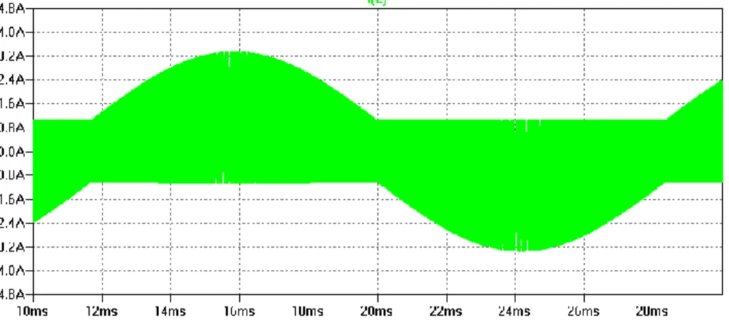
In order to verify the proposed Dynamic Dead Time Optimization technique, Linear Technology’s LTspice simulation software was used to simulate a half-bridge single-phase 130W inverter operating with BCM ZVS current control. The simulation circuit parameters are as follows: DC bus voltage 400 V, AC grid voltage 120 V rms, 60 Hz, inductor value 270 µH and switching frequency range 20-185 kHz. The high frequency current in the filter inductor with 60 Hz modulation is shown in Figure 2-10.
Figure 2-10: Inductor current with BCM current control and fixed reverse current.
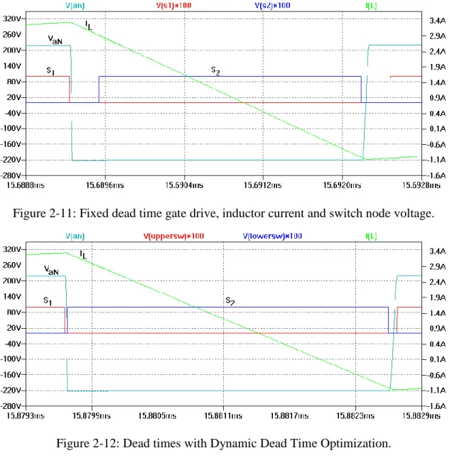
Figure 2-11 shows filter inductor current, MOSFET gate drive voltages and switch node voltage (VaN) with a fixed turn-on and turn-off dead time of 300 ns at the peak of the grid current.
The simulation waveforms in Figure 2-12 depict how Dynamic Dead Time Optimization independently changes the gate drive turn-on and turn-off dead time. Once the MOSFET parasitic
25
capacitors are fully charged/discharged, the dynamic dead time optimization controller enables the gate drive, thereby minimizing MOSFET body diode conduction time.
Figure 2-11: Fixed dead time gate drive, inductor current and switch node voltage.
Figure 2-12: Dead times with Dynamic Dead Time Optimization.
2.6 Advanced Phase Skipping Control
In three-phase inverters and microinverters, it is advantageous to operate at or close to rated power where efficiency is the highest. However, when power levels drop, the available power is distributed evenly among the three phases. This results in reduced efficiency because load
26
independent loss will become a bigger portion of the overall losses. In single-phase inverters, techniques such as pulse skipping [50] are commonly employed in an effort to improve light-load efficiency. This method is not predictable and can become problematic in large installations. Advanced Phase Skipping Control maximizes the output stage efficiency of a three-phase micro-inverter by managing the amount of power on each phase based on the available power [51]. The available power is determined by the PV side MPPT controller.
In an Advanced Phase Skipping system, there are three possible modes of operation: normal three-phase mode, two-three-phase mode and single-three-phase mode. The controller transitions between these three modes in order to maximize inverter efficiency. Based on the available power, the controller can disable one or two phases of the three-phase system. At power levels above two-thirds of rated power, all three phases are enabled. At one-third to two-thirds of rated power, the controller disables one phase. At power levels below one-third of rated power, the controller enables only one phase. It should be noted that in single and two-phase modes, the ripple current in the DC link capacitor will be considerably higher. This problem is mitigated by the fact that in this mode the power level is much less and the controller can compensate for this by adjusting the DC link voltage to ensure that there is enough headroom to run the output stage.
Available power may vary over a wide range during a typical day due to environmental factors such as clouds and shading as well as low irradiance during morning and afternoon. During times when available power is low, the three-phase micro-inverter will most likely be operating in single-phase mode. As available power increases during the day, the controller will enable two and eventually all three phases and distribute power evenly in each phase in order to maximize overall system efficiency.
27
Unlike phase shedding techniques employed in multiphase converters commonly used in Voltage Regulator Modules (VRMs) and interleaved Power Factor Correction (PFC) circuits, in an Advanced Phase Skipping system, the overall number of operating phases does not change and in fact this control technique is used to maintain three-phase system balance. Actual phase skipping is done at the micro-inverter level in order to maintain the integrity of all three phases at the system level. However, the overall strategy would require a system level controller to dynamically manage the power from each micro-inverter to ensure power imbalance between the three phases is minimized.
2.7 Experimental Results
Experimental results were obtained from a 400-W three-phase half-bridge micro-inverter prototype using two different manufacturer’s MOSFETs for switching devices. The MOSFETs specifications are included in Table 2-1 for reference. MOSFETs with large differences in COSS were chosen for this work in order to demonstrate the effectiveness of the proposed Dynamic Dead Time Optimization for a wide range of MOSFET parasitic capacitors. The DSP used is a Microchip dsPIC33FJ16GS504. The experimental circuit parameters are as follows: DC bus voltage 400 V, AC grid voltage 120 V rms, 60 Hz, inductor value 270 µH and switching frequency range 20-185 kHz. Using equations (2-10) and (2-11) in MATLAB, a lookup table can be generated which contains the optimum dead time values for each circuit operating point. This table can then be programmed into the DSP where the optimum dead time values are selected based on the DSP’s measurement of dynamic circuit operating parameters.
28
Table 2-1: Two Different Manufacturer’s MOSFETs Specifications Manufacturer Part Number Vdss (V) Id (A) Rds-ON (Ω) Ciss (pF) Coss (pF) Crss (pF) VSD* (V) FCB20N60F 600 20 0.150 2370 1280 95 1.4 STB21N65M5 650 17 0.150 1950 46 3 1.5
* Drain to Source Diode Forward Voltage
The experimental waveforms of Figures 2-13, 2-14 and 2-15 correspond to Figures 2-10, 2-11 and 2-12 in the simulation results respectively.
Figure 2-13: Filter inductor current.
29
Figure 2-15: Experimental waveforms with Dynamic Dead Time Optimization.
The micro-inverter was tested in four different modes of operation: normal operation (with fixed dead time and no phase skipping), with Dynamic Dead Time Optimization (DTO) only, with Advanced Phase Skipping Control only, and with both Dynamic DTO and Advanced Phase Skipping Control.
Figures 2-16 and 2-17 show the efficiency measured with a Yokogawa PZ4000 power analyzer for each of the micro-inverter operating modes for FCB20N60F and STB21N65M5 MOSFETs respectively.
30
Figure 2-17: Micro-inverter output stage efficiency with STB21N65M5 MOSFET.
Referring to the efficiency figures, it can be seen that both manufacturer’s MOSFETs exhibited similar performance with respect to each of the four micro-inverter operating modes. Efficiency was the lowest over the entire load range when the micro-inverter was operated in normal mode for both manufacturer’s MOSFETs. A noticeable improvement in efficiency was achieved by implementing Dynamic Dead Time Optimization. Efficiency improvement was the highest at light loads where switching frequency is maximum. Implementing Advanced Phase Skipping Control also resulted in significant efficiency improvement especially at light loads. The best efficiency was realized with a combination of Dynamic Dead Time Optimization and Advanced Phase Skipping Control. CEC weighted efficiency is shown in Table 2-2 for both manufacturer’s MOSFETs and for each mode of operation.
31
Table 2-2: CEC Weighted Efficiency for Different Modes of Operation Manufacturer Part Number Normal Operation (Fixed Dead Time) Dynamic DTO Advanced Phase Skipping Control Dynamic DTO + Advanced Phase Skipping Control FCB20N60F 96.96% 98.06% 97.67% 98.42% STB21N65M5 96.21% 97.97% 97.35% 98.48%
Combining Dynamic Dead Time Optimization and Advanced Phase Skipping Control produced an additional 1.5 percentage points in CEC efficiency for FCB20N60F MOSFET and 2.3 percentage points in CEC efficiency for STB21N65M5 MOSFET.
It is worth noting that neither of the two efficiency improvement techniques described in this chapter require any additional circuit components. Therefore, reliability and cost will not be negatively impacted and in fact reliability will be improved due to lower operating junction temperatures. Research on reliability of power MOSFETs and predicting their failures shows that it is possible to predict failure of power MOSFETs due to thermal stress without estimating the junction temperature [52], [53]. This is achieved by developing a mathematical framework to capture the drop in on voltage of a MOSFET due to aging and developing prognostic models [54]. Although advanced phase skipping control is applicable only to three-phase inverters and micro-inverters, dynamic dead time optimization will improve efficiency of both three-phase and single-phase inverters and micro-inverters that employ soft switching techniques such as BCM ZVS current control.
32
2.8 THD Improvement with Dynamic Dead Time Optimization
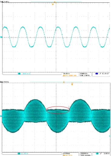
Since optimizing the dead time minimizes inductor current excursion beyond the upper and lower fixed reverse thresholds in BCM ZVS current control, an improvement in THD is realized. Figure 2-18 shows output current and inductor current at 80 W with fixed dead time. It can be seen that the reverse current threshold is not constant and in fact varies with the peak current. This anomaly tends to increase THD by subtracting from the output peak current.
Figure 2-18: Output current and inductor current with fixed dead time.
The THD in Figure 2-18 is 7.78% measured with a Yokogawa PZ4000 power analyzer. This effect is more significant at light loads since the fixed dead time becomes a larger portion of the switching
33
period. Identical conditions with implementation of Dynamic Dead Time Optimization control is shown in Figure 2-19. The anomaly shown in Figure 2-18 is greatly reduced due to the fact that dead time is now proportional to the switching period resulting in a much improved THD of 4.74%.
Figure 2-19: Output current and inductor current with dynamic dead time optimization.
2.9 Summary
In this chapter, two efficiency improvement techniques have been introduced and implemented in a three-phase micro-inverter. Practical implementation of these two techniques has been verified by experimental results on a 400-W three-phase micro-inverter prototype. It is very important to
34
note that no additional circuit components are required and the techniques can be implemented entirely in the digital controller firmware.
Dynamic Dead Time Optimization minimizes MOSFET body diode conduction time which reduces power dissipation. Therefore, reliability will be improved due to lower operating junction temperatures. THD will also be improved in inverters using BCM ZVS current control. This technique can be digitally implemented on three-phase and single-phase inverters and micro-inverters that employ soft switching techniques. Advanced Phase Skipping Control is applicable to three-phase inverters and micro-inverters. Depending on the available input power from the PV source, this control method features distributed power to individual phases so that the maximum DC/AC stage efficiency of the three-phase micro-inverter is achieved. The experimental results show that the proposed hybrid digital control algorithm which combines Dynamic Dead Time Optimization and Advanced Phase Skipping Control can significantly improve the CEC efficiency of a 400-W three-phase half-bridge micro-inverter prototype.
35
CHAPTER 3.
ANALYSIS AND OPTIMIZATION OF
VARIABLE-FREQUENCY SOFT-SWITCHING PEAK CURRENT MODE
CONTROL TECHNIQUES FOR MICROINVERTERS
3.1 Introduction
This chapter presents a detailed power loss model for a microinverter with three different zero voltage switching (ZVS) boundary conduction mode (BCM) current modulation methods. The model is used to calculate the optimum peak current boundaries for each modulation method. Based on the power loss model, a dual-zone modulation method is proposed to further improve the microinverter efficiency. The proposed modulation method provides two main benefits: the addition of one more soft switching transition and low inductor peak current. The additional soft switching transition reduces switching losses by means of zero current switching (ZCS). The lower peak current boundary reduces inductor rms current and conduction losses as well as allowing the output filter inductor to be smaller and more efficient. An improved BCM peak current control method was proposed and implemented on a microinverter prototype. The control circuit provides a highly accurate representation of the filter inductor current waveform and also provides galvanic isolation which simplifies control circuit design. The experimental results on a 400-W three-phase half-bridge microinverter validate the theoretical analysis of the power loss distribution and demonstrate that further improvement in efficiency can be achieved by using the proposed dual-zone modulation method.
36
3.2 Variable-Frequency Peak Current Mode Control Techniques
Three ZVS BCM peak current mode control methods are described and compared in this section. Figure 3-1 depicts a standard power circuit of a three-phase half-bridge inverter. The body diode and the parasitic capacitance of the MOSFETs help to achieve ZVS in an inverter output stage. In order to implement turn-on ZVS, the bidirectional inductor current discharges the MOSFET parasitic capacitance until its body diode conducts prior to each switching transition.
Figure 3-1: Three-phase half-bridge inverter.
In order to inject AC current into the grid, the average inductor current must be equal to the reference current during each switching cycle. Therefore, the inductor current has to be between two predetermined boundaries. Three current modulation methods with different boundary shapes have been introduced in [35] which satisfy this requirement: BCM with fixed reverse current, BCM with variable reverse current, and BCM with fixed bandwidth.
As shown in Figure 3-2, the inductor current has to be between the upper and lower limits for all the three modulation techniques in order to generate an average current equal to the reference
37
current. Since the inverter power loss is to be analyzed in this chapter, the inductor current and switching frequency are calculated for each of the three modulation techniques.
(a)
(b)
(c)
Figure 3-2: Three different ZVS BCM modulation methods: (a) fixed reverse current, (b) variable reverse current, (c) fixed band width.
38
The upper and lower boundaries and switching frequency for BCM with fixed reverse current modulation can be calculated as follows:
{𝐼𝑢𝑝𝑝𝑒𝑟 = 2𝐼𝑅𝐸𝐹sin(𝜔𝑡) + 𝐼𝑜 𝐼𝑙𝑜𝑤𝑒𝑟 = −𝐼𝑜 , if sin (𝜔𝑡) ≥ 0 ( 3-1 ) {𝐼𝑢𝑝𝑝𝑒𝑟 = 𝐼𝑜 𝐼𝑙𝑜𝑤𝑒𝑟 = 2𝐼𝑅𝐸𝐹sin(𝜔𝑡) − 𝐼𝑜 , if sin (𝜔𝑡) < 0 𝑓𝑠𝑤(𝑡) = ( 𝑉𝑑𝑐 2 ⁄ )2−(𝑉𝑚sin (𝜔𝑡))2 𝐿𝑉𝑑𝑐(2𝐼𝑅𝐸𝐹sin (𝜔𝑡)+2𝐼𝑜) ( 3-2 )
where, IREF is the output peak current reference, Io is the reverse current for achieving ZVS, Vdc is the input voltage for the half-bridge inverter, Vm is the grid or output peak voltage and L is the output filter inductor.
The boundaries and switching frequency for BCM with variable reverse current modulation can be found from equations (3-3) and (3-4).
{ 𝐼𝑢𝑝𝑝𝑒𝑟 = 3 2𝐼𝑅𝐸𝐹sin(𝜔𝑡) + 𝐼𝑜 𝐼𝑙𝑜𝑤𝑒𝑟 = 1 2𝐼𝑅𝐸𝐹sin(𝜔𝑡) − 𝐼𝑜 , if sin (𝜔𝑡) ≥ 0 ( 3-3 ) { 𝐼𝑢𝑝𝑝𝑒𝑟 = 1 2𝐼𝑅𝐸𝐹sin(𝜔𝑡) + 𝐼𝑜 𝐼𝑙𝑜𝑤𝑒𝑟 = 3 2𝐼𝑅𝐸𝐹sin(𝜔𝑡) − 𝐼𝑜 , if sin (𝜔𝑡) < 0 𝑓𝑠𝑤(𝑡) = (𝑉𝑑𝑐 2 ⁄ )2−(𝑉𝑚sin (𝜔𝑡))2 𝐿𝑉𝑑𝑐(𝐼𝑅𝐸𝐹sin (𝜔𝑡)+2𝐼𝑜) ( 3-4 )
The upper and lower limits and switching frequency for BCM with fixed bandwidth modulation can be expressed as follows:
39 {𝐼𝑢𝑝𝑝𝑒𝑟 = 𝐼𝑅𝐸𝐹sin(𝜔𝑡) + 𝐼𝑜 𝐼𝑙𝑜𝑤𝑒𝑟 = 𝐼𝑅𝐸𝐹sin(𝜔𝑡) − 𝐼𝑜 , if sin (𝜔𝑡) ≥ 0 {𝐼𝑢𝑝𝑝𝑒𝑟 = 𝐼𝑅𝐸𝐹sin(𝜔𝑡) + 𝐼𝑜 𝐼𝑙𝑜𝑤𝑒𝑟 = 𝐼𝑅𝐸𝐹sin(𝜔𝑡) − 𝐼𝑜 , if sin (𝜔𝑡) < 0 ( 3-5 ) 𝑓𝑠𝑤(𝑡) = (𝑉𝑑𝑐 2 ⁄ )2−(𝑉𝑚sin (𝜔𝑡))2 𝐿𝑉𝑑𝑐(2𝐼𝑜) ( 3-6 )
Note that for all three modulation methods, T1 and T2 are the required time for inductor current to traverse from the lower limit to the upper limit and from the upper limit to the lower limit,
respectively and calculated as follows:
{ 𝑇1 = 𝐿(𝐼𝑢𝑝𝑝𝑒𝑟−𝐼𝑙𝑜𝑤𝑒𝑟) (𝑉𝑑𝑐 2 ⁄ )−𝑉𝑔𝑟𝑖𝑑 𝑇1 =𝐿(𝐼𝑢𝑝𝑝𝑒𝑟−𝐼𝑙𝑜𝑤𝑒𝑟) (𝑉𝑑𝑐 2 ⁄ )+𝑉𝑔𝑟𝑖𝑑 ( 3-7 )
Switching frequency is derived from (3-7) as follows:
𝑓𝑠𝑤 = (𝑉𝑑𝑐
2
⁄ )2−(𝑉𝑔𝑟𝑖𝑑)2
𝐿𝑉𝑑𝑐(𝐼𝑢𝑝𝑝𝑒𝑟−𝐼𝑙𝑜𝑤𝑒𝑟) ( 3-8 )
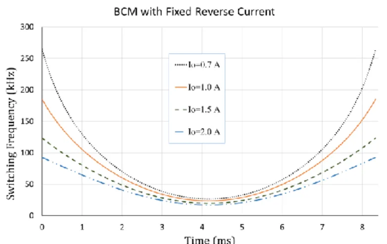
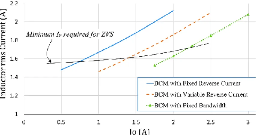
The switching frequency and inductor rms current are determined by the peak current boundaries. Figures 3-3 and 3-4 depict the full load switching frequency and inductor rms current for each modulation method at different boundary values. An output inductor value of 270 μH was selected to ensure that the minimum switching frequency was above the maximum audible value of 20 kHz.
40 (a)
(b)
(c)
Figure 3-3: Switching frequency over a half 60-Hz line cycle with varying Io for: (a) fixed reverse current, (b) variable reverse current, and (c) fixed band width.
41
Figure 3-4: Inductor rms current versus Io for each modulation method at full load.
Referring to equations (3-2), (3-4) and (3-6), switching frequency for all three modulation methods is a function of the grid or output voltage and the peak current boundaries and is the highest at zero crossings. For example, BCM with fixed reverse current has the widest switching frequency range because both the instantaneous output voltage and the peak current boundaries decrease at zero crossings. BCM with fixed bandwidth has the narrowest switching frequency range since its peak current boundaries are constant over the entire output voltage range. Likewise, at full load, BCM with fixed reverse current has the lowest inductor rms current, while BCM with fixed bandwidth has the highest inductor rms current.
The minimum reverse current for achieving ZVS depends on the MOSFET’s specification (parasitic capacitance, COSS), the voltage across the MOSFET (Vdc) and dead time (td), and for this topology is approximately calculated as follows [55]:
𝐼min_𝑍𝑉𝑆_𝑟𝑒𝑣𝑒𝑟𝑠𝑒_𝑐𝑢𝑟𝑟𝑒𝑛𝑡≈ 2𝐶𝑂𝑆𝑆𝑉𝑑𝑐
𝑡𝑑 ( 3-9 )
An optimum combination of dead time (800 ns) and reverse current (0.8 A) was selected experimentally for this work. Therefore, in order to ensure ZVS operation for each modulation method, a minimum reverse current of 0.8 A is required to discharge the MOSFET parasitic
42
capacitance. With this in mind, the minimum Io required to maintain the 0.8 A reverse current for each modulation method at full load is shown in Figure 3-4. In all three modulation methods, ZVS is achieved during the entire grid cycle. Therefore, for each modulation Io is determined in such a way that ZVS can even be achieved for the lowest reverse current.
Since only turn-on ZVS can be achieved with these modulation methods, higher switching frequency generally results in proportionally higher switching losses. Larger boundary values reduce switching frequency but also increase inductor rms current and conduction losses.
A detailed power loss analysis will be presented in the next section which determines the optimum boundary values for each modulation method in order to maximize efficiency.
3.3 Power Loss Analysis
A loss model was designed in order to predict the power loss in the three-phase half-bridge microinverter prototype. Table 3-1 shows the prototype operating parameters. This model can be used to calculate the most efficient peak current boundary for each of the three modulation methods. Four sources of loss have been taken into consideration in this model: switching loss (including MOSFET body diode conduction loss), MOSFET conduction loss, inductor core loss and inductor winding loss.
Since all three modulation methods can achieve turn-on ZVS, only turn-off switching loss is calculated in the loss model using the following equation:
𝑃𝑠𝑤(𝑂𝐹𝐹)(𝑡) =1
43
Table 3-1: Inverter Prototype Operating Parameters
Grid parameters
Output power Input Voltage Switching devices Output capacitor Main inductor
Vgrid (nominal) = 120Vrms(Line-Neutral)
208Vrms(Line-Line)
fgrid (nominal) = 60 Hz
Po = 130 W (each phase)
Vdc = 400 V (+200V, -200V)
Fairchild FCB20N60F MOSFET
Co = 1µF polypropylene film (each phase)
L = 270 µH (each phase), peak current= 4.5 A
Rdc = 85 mΩ, magnetic core RM12/N95 ferrite,
wire: Litz, 60 strands #38, 36.5 turns, air gap = 0.86 mm
where, Ii (i=1, 2) is the peak boundary current for the upper and lower MOSFETs, respectively,
VDS is the MOSFET drain-source voltage, fSW(t) is the instantaneous switching frequency and t
S(H-L) is the MOSFET turn-off time.
To avoid shoot through current between the MOSFETs, dead time is included in the complementary gate drives. During the dead time, the MOSFETs body diode conducts which results in power loss and is calculated as follows:
𝑃𝐵𝐷(𝑡) = 𝐼𝑖(𝑡)×𝑉𝑆𝐷×𝑓𝑠𝑤(𝑡)×(𝑡𝑑1 + 𝑡𝑑2) ( 3-11 ) where, VSD is the diode forward voltage drop, td1 and td2 are the upper and lower MOSFET body diode conduction times, respectively.
![Figure 1-5: DC link voltage control using a digital finite impulse response (FIR) filter [36]](https://thumb-us.123doks.com/thumbv2/123dok_us/762514.2596470/25.918.198.730.253.608/figure-voltage-control-digital-finite-impulse-response-filter.webp)
![Figure 1-7 shows voltage ripple estimation method proposed by Ninad and Lopes [38]. In an effort to mitigate the effect of DC link voltage ripple on the inverter output current, voltage ripple is estimated to be added to the DC link reference volt](https://thumb-us.123doks.com/thumbv2/123dok_us/762514.2596470/26.918.163.764.772.1026/figure-voltage-estimation-proposed-mitigate-inverter-estimated-reference.webp)