ScholarWorks
Materials Science and Engineering Faculty
Publications and Presentations Department of Materials Science and Engineering
1-1-2018
Improving the Relative Calculations of Volta
Potential Differences Acquired from Scanning
Kelvin Probe Force Microscopy (SKPFM) from
Comparing an Inert Material to First-Principle
Calculations
C. M. Efaw Boise State University T. da Silva Boise State University P. H. Davis Boise State University L. Li
Boise State University E. Graugnard Boise State University
© The Electrochemical Society, Inc. 2018. All rights reserved. Except as provided under U.S. copyright law, this work may not be reproduced, resold, distributed, or modified without the express permission of The Electrochemical Society (ECS). The archival version of this work was published inECS Transactions,85(13), 701-713. doi:10.1149/08513.0701ecst
C. M. Efaw, T. da Silva, P. H. Davis, L. Li, E. Graugnard, and M. Hurley
Improving the Relative Calculations of Volta Potential Differences Acquired from Scanning Kelvin Probe Force Microscopy (SKPFM) from Comparing an Inert
Material to First-Principle Calculations
C.M. Efawa, T. da Silvaa, P. H. Davisa, L. Lia, E. Graugnarda, and M. Hurleya
a Micron School of Materials Science and Engineering, Boise State University, Boise, ID
83706, USA
An improved relative scaling of Volta potential differences (VPD) acquired from scanning Kelvin probe force microscopy (SKPFM) was developed by quantifying the probe work function. In corrosion studies, SKPFM has been used to identify local nobility of complex metallic systems and provide theoretical corrosion initiation sites. However, large variability in measured VPD values for metallic phases has led to controversy in their interpretation. Tracking changes of the probe work function has been shown to decrease the variability seen in SKPFM results. To quantify the work function of SKPFM probes, the measured VPD of an inert gold standard was compared to the work function theoretically calculated by density functional theory (DFT) first-principles. For proof of concept, a stainless steel sample joined by a Cu-Ag-Ti brazing material was characterized by SKPFM with three different types of probes.
Introduction
The Kelvin probe is a tool utilized to measure electronic properties of a sample surface relative to a conductive probe. By combining the Kelvin probe with atomic force microscopy (1-2), the resulting scanning Kelvin probe force microscope (SKPFM) technique has been able to produce maps of relative electronic activity that correspond to compositional difference between phases present on a material surface. Used as a low- to non-destructive tool in either ambient or controlled conditions, SKPFM can spatially resolve nanometer scaled surface phases (3-5). The scanning Kelvin probe technique has been utilized as a characterization tool in a wide range of applications including semiconductor (4-6) and electrical device characterization (7-8), as well as corrosion studies (9-14).
SKPFM presents spatial maps of surface Volta potential differences (VPD or ¨ȥ). In air, the Volta potential difference can be calculated theoretically from the difference in modified (not in vacuum) work functions between the metallic sample surface (M) and the probe (P), which acts as a pseudo reference.
ο߰ெ ൌ ߰ெെ ߰ ൌ ሺ߮ெ െ ߮ሻȀ݁(3, 15) [1]
In equation 1, ȥ is Volta potential, ij is work function, and e is electron charge. It is important to distinguish that the Volta potential difference is the relative difference in modified work function between the sample surface and the pseudo reference probe used
for the imaging. Quantifying the probe work function allows the modified work function of phases on a sample surface to be theoretically calculated from equation 1 and mapped
VPD values. However, calculation of the pUREH¶V ZRUN IXQFWLRQ LV RYHUORRNHG.
Comparisons between results have been limited to either a pseudo or a non-quantified relative scale, causing large variations in reported VPD values, and at times differences in
LQWHUSUHWDWLRQRIYDULRXVSKDVHV¶IXQFWLRQDOLW\ in specific conductive materials.
Though the techniques presented in this work can be used generally to interpret SKPFM data, the focus of this work is driven by the inconsistencies reported in corrosion studies. Broadly, it has been shown that there is a direct correlation between PDWHULDOV¶VPD values and their open circuit potentials (16-18). SKPFM has thus been able to provide a theoretical mapping of local phase nobility for complex metallic systems (19-23), as well as ex situ measurements following periods of exposure to corrosive mediums (24-25). A notable lack of reproducibility of Volta potential differences has been discussed for different alloy series (15, 19), and though much of previously reported work has been able to distinguish phase nobility for individual maps, subsequent mapping and other work are not discretely comparable (19). This divergence in experimental data found in literature has led to differing concluding remarks when investigating the corrosion mechanisms of certain metal alloys (15, 19, 26).
Recently, high resolution computational simulations have shown that the crystallographic orientation, as well as the terminating atom of the material surface, can drastically affect the observed work function and the Volta potential difference (15, 27). There is also notable shifts in SKPFM measured relative Volta potential differences that are caused by metal passivation and adsorbed species (28-29). Computational outputs can provide experimentalists with a directory of theoretical work function values for various phases within a metal alloy. Comparison of plausible work function values for a particular phase with the resulting Volta potentials seen from SKPFM mapping can provide improved interpretation of the corrosion mechanisms for the alloy.
Though this evidence provides reason for variations in VPD values, the observation in probe choice and how that drives uncertainty in data acquisition is still lacking in current literature. Uncertainty can come from the material make-up and design of the probe, as well as progressive wear and chemical changes (i.e. oxidation or adsorbed species) of a probe from extended usage. These sources of uncertainty will ultimately affect the resulting VPD acquired without there being any actual deviation in the composition of the sample surface. Therefore, it is seen that the probe can be a causation to the large range of reported Volta potential difference values in literature. However, probe choice, as well as progressive wear of the probe, is commonly overlooked when presenting SKPFM results. Recently, redesign of SKPFM probes has been able to address these uncertainties, showing consistent initial VPD results for many probes of the same type (30). Though the improvement in probe design has shown greater consistency for initial probe usage, this work hopes to address uncertainty of probe work function from progressive wear by utilizing an inert standard as a reference material prior to imaging a material of interest.
In typical three-electrode electrochemical testing (i.e. polarization testing or impedance spectroscopy), all potential values are presented relative to a reference electrode (i.e. saturated calomel electrode). Similarly, a comparable practice has been done with SKPFM, wherein the pseudo reference probe is replaced with a relatively inert material as a
reference for scaling Volta potential values (3, 16, 24, 31). Herein results are presented both on a relative scale versus an inert standard, but also theoretical work functions are calculated for the phases present on the sample surface.
Experimentation
SKPFM was used to generate surface VPD maps. Imaging presented in this work was carried out on a Nanoscope V Bruker Dimension Icon AFM, where operation was done with two different modes. The modes chosen were based upon the compatible design of the probe used for imaging. The first utilized tapping-mode with frequency modulation (FM-KPFM) in a single-pass method, wherein both topography and surface potential are acquired simultaneously. Frequency modulation is detected from variations in the electric force gradient between the probe and surface. The electric force gradient will cause a shift in the resonant frequency of the probe, producing side bands. The sidebands are typically only a few kHz above and below the resonant frequency, where the amplitude of the sidebands provide the magnitude of frequency modulation. With a DC biasing for nullification, this KPFM feedback mechanism can provide the user with relative VPD values.
The second technique also utilizes frequency modulation for acquiring VPD maps; however, topography is acquired separately with PeakForce tapping mode (Bruker, Santa Barbara, CA, USA), trademarked as PF-KPFM. Within this operation, the probe completes a dual-pass interaction with the sample surface, where line-by-line topography and Volta potential difference values are sequentially acquired. For the first pass, topography is acquired by intermittent contact with the sample surface from rapidly generating force curves at 2 kHz frequency. The feedback mechanism is controlled by a user-defined peak force recurring between the probe and sample surface (5-20 nN during this study). Upon completing a single trace and retrace line of topography, the probe lifts off the surface at a user-defined lift height and retraces the line of topography. During the second trace and retrace, VPD measurements are acquired by the frequency modulation method previously described. This is accomplished at a constant surface-probe distance to prevent effects of topographical artifacts in mapping of the Volta potential difference (30, 32). A lift height of 100 nm was used to sufficiently avoid artifacts caused by sudden tip-sample contact.
Imaging was done with three different types of probes. First was PFQNE-Al (Bruker), made up of a silicon tip of nominally 5 nm radius with a proprietary reflective coating on the backside of the cantilever. Second was SCM-PIT (Bruker), made up of an antimony (n) doped silicon probe with a platinum/iridium coating on both the tip (nominally having a 20 nm radius post-coating) and cantilever. Lastly, imaging was also conducted with 25Pt300B (Rocky Mountain Nanotechnology, Salt Lake City, UT, USA), a solid platinum probe of nominally a 20 nm tip radius with the cantilever connected to a conductive gold bonding pad by conductive epoxy. Due to their relatively low spring constant, PFQNE-Al and SCM-PIT probes are well-designed to operate in PF-KPFM mode (29). Alternatively, 25Pt300B probes, due to a higher spring constant and larger cantilever, would operate best in the FM tapping-mode. Therefore, with this experimentation, not only is the effect of probe selection being observed, but also the mode of operation.
Probe velocity of 3 to 20 µm/s were used in this work, basing this rate on the roughness of the sample being imaged and desired signal to noise effects. Topographical lateral resolution is controlled by the number of probe-surface interactions acquired per length of scan size, ranging in this work from 5 to 40 nm. Imaging was completed in ambient atmospheric conditions of 69-73oF temperature and 40-60% relative humidity. The inert standard used for this study is the Bruker KPFM standard (Bruker, Santa Barbara, CA, USA), consisting of an n-doped silicon wafer patterned with 50 nm thick sections of aluminum and gold, where small sections of exposed underlying wafer separate the aluminum and gold sections. From here on, the Bruker KPFM standard will be designated as the Al-Si-Au standard.
SKPFM results for the standard were compared to work function calculations from first-principle density functional theory (DFT) calculations (33-34). Atomic structures were constructed as defined by their known crystal structure parameters. Atomic and electronic structures were calculated using Vienna ab initio simulation package (VASP) (35) with the projector augmented wave (PAW) method (36). The Perdew-Burke Ernzerhof (PBE) (37) form of the generalized gradient approximation (GGA) (38) was used for the exchange-correlation potential to address electron-electron interaction. Plane-wave expansion of the wave function was performed with the PAW method and a cutoff energy of 450 eV. Brillouin zone integration was performed on a 9x9x1 gamma-centered mesh for all the slab structures. Periodic slabs of these structures (Figure 1) were built large enough for convergence of the calculated work function, and a vacuum of 20 Å was built large enough to avoid unphysical interactions with neighboring slabs. The vacuum energy level (ܧ௩) and Fermi energy level (ܧி) were obtained for each structure. The theoretical work function (߮) is calculated using equation 2. Work function values for aluminum, gold, and silicon surfaces were obtained for the (100), (110), and (111) planes, and averaged to compare with SKPFM results.
߮ ൌ ܧ௩ െ ܧி [2]
Figure 1. (Left to right) Aluminum, silicon, and gold crystal structures oriented with the (100) face exposed to a vacuum of 20 Å.
The exemplary sample of interest used for this work is a separated disk-shaped 316L stainless steel sample rejoined by a Cu-Ag-Ti braze alloy. Joints formed by brazing offers as an alternative to common joining techniques, such as mechanical fastening and welding. The sample is further described elsewhere (20). The sample was polished with progressively finer silicon carbide pads from 400 to 1200 grit. Following SiC polishing,
the sample was polished with 1 µm and 0.05 µm alumina slurries. Following each polishing step, the sample was rinsed with DI water, ethanol, and then dried with compressed air. Prior to imaging with SKPFM, the sample was cleaned by ultrasonication in a bath of non-denatured ethanol. The effect of polishing and sample preparation on Volta potential differences has been previously observed (28). To minimize these effects on the acquired VPD values, the sample was consistently prepared in a similar manner for each imaging session.
Prior to imaging with SKPFM, an electrical connection between the sample surface and the AFM stage was established using colloidal silver paint and verified with a voltmeter. The Al-Si-Au standard was imaged both prior to and following imaging of the brazed steel sample to ensure calibration and consistency of the probe. Imaging of the brazed steel sample then allows the user to calculate theoretical work functions of the phases seen on the material surface.
Results and Discussion Calculated Work Functions from Density Functional Theory
The work functions of pure gold, aluminum, and silicon were determined from DFT calculations. Table I summarizes the values found, which are comparatively similar to work functions found in literature (15, 39-42). The substrate of the Al-Si-Au standard is an n-doped silicon wafer, expectedly having a lower work function than pure silicon. Also, when exposed to an oxygen-enriched environment, both aluminum and silicon are highly reactive and form passive oxide films, thus increasing their surface work functions (28-29). These variations and unknowns in the physical nature of the aluminum and silicon could contribute to a difference between calculated work function values and the experimentally measurable work function observed with SKPFM. Gold, being a relatively inert substance, was assumed to have no adsorbed species on its surface, and thus should ultimately have the most comparable work function between theoretical calculations and experimental measurements.
TABLE I. Calculated WF values for the Al-Si-Au standard averaged over relevant planes.
Material Face Vacuum Energy Ev (eV) Fermi Energy EF (eV) Work Function ij (eV) Average Work Function (eV) Aluminum (100) 4.643 0.427 4.22 4.11 (110) 2.971 -1.089 4.06 (111) 4.924 0.886 4.04 Silicon (100) 3.710 -1.608 5.32 4.94 (110) 3.101 -1.703 4.80 (111) N/A N/A 4.71 (30) Gold (100) 4.770 -0.324 5.09 5.07 (110) 2.590 -2.410 5.00 (111) 3.357 -1.759 5.12
Quantifying Probe Work Function
Prior to SKPFM imaging of the Cu-Ag-Ti brazed steel, the Al-Si-Au standard was
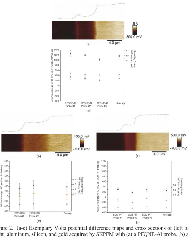
maps of the Al-Si-Au standard are shown in Figure 2(a-c). As stated in the previous section, both aluminum and silicon have plausible reasons of variability in their composition, and thus were not selected as final reference materials. Therefore gold was chosen as the reference material to quantify the work function of an operating probe. This is due to its relatively low reactivity and greater likelihood of providing accurate results over aluminum and silicon. The step-wise shift in Volta potential differences from aluminum to silicon to gold can still be used as a relative tracking of probe consistency, as well as observing spatial
UHVROXWLRQ RI WKH SUREH¶V HOHFWURQLF DFWLYLW\ (such as contribution from the conductive material on both the probe¶s tip and its cantilever) by looking at the slope between sections of the Al-Si-Au standard (30, 32).
Figure 2(d-f) presents the average and standard deviation VPDs determined from twelve different images with each probe. The Volta potential difference between the probes and goldሺο߰௨) acquired by SKPFM is observed from the difference of work functions between the gold surface (߮௨) and the probe (߮). The work function of gold acquired by DFT calculations is 5.07 eV (Table I). From there, a relative work function of the operating probe can be found. This is presented on the right y-axes, where the resulting probe work function is shown as partial axes.
The variation between sets of images exemplifies a realistic use of SKPFM probes, where the same probe may be used on multiple occasions with progressive wear before being replaced by a new probe. The average VPD values for the Al-Si-Au sections are notably different for the three different probe types (PFQNE-Al, Pt300B, and SCM-PIT), providing a range of approximately 1070 mV, or 1.07 eV. This drastic difference in acquired data provides one plausible explanation as to why there has been such a large variation in reported VPD results in literature, and emphasizes the importance in describing the type of probe that is used when presenting VPD results.
Analyzing the data from Figure 2 also shows that probe choice makes a drastic difference for the specific SKPFM technique that is chosen. It can be seen that the standard deviation for the PFQNE-Al and SCM-PIT probes (using PF-KPFM) is much less than the standard deviation for the 25Pt300B probes (using tapping-mode FM-KPFM). This is partly due to the design of the probes. Also of note is the ease of operating with PF-KPFM over FM-KPFM. Unlike in tapping mode, with PeakForce tapping the amount of force applied on the surface can be controlled, and thus the wear on the probe can be lessened.
Although the relative variation seen for each of the three PFQNE-Al and the three SCM-PIT probes is lower than seen with the two 25Pt300B probes, there is still a notable difference in average VPD and resulting probe WF. Most notably, PFQNE-Al probe #1 measured an average gold VPD of 1250 mV, whereas PFQNE-Al probe #3 measured an average gold VPD of 1025 mV. Also, of the thirty six total images acquired by the three PFQNE-Al probes, the resulting VPD values for gold covered a range of ~500 mV, or 0.5 eV in resulting probe WF. Likewise, imaging with the SCM-PIT probes provided a range of ~275 mV, or 0.275 eV in resulting probe WF. This variation between probes of similar chemical make-up and design gives rise to the need for probe work function quantification prior to SKPFM imaging of a material, regardless if similar probe choice is done between different sets of work. This necessity will be further described in the following section.
Figure 2. (a-c) Exemplary Volta potential difference maps and cross sections of (left to right) aluminum, silicon, and gold acquired by SKPFM with (a) a PFQNE-Al probe, (b) a 25Pt300B probe, and (c) a SCM-PIT probe. (d-f) Data results from imaging of aluminum (silver circle), silicon (orange triangle) and gold (blue square) with (d) three different PFQNE-Al probes, (e) two different Pt300B probes and (f) three different SCM-PIT probes. Relative Work Functions of Different Phases
2QFHWKHSUREH¶VZRUNIXQFWLRQLVTXDQWLILHG on a relative scale, the material of interest can accurately be imaged with SKPFM. Imaging was completed on a readily available material with nanoscale complexity, yet ease of recognizing phase separation, to present feasibility of this technique. The representative sample for this work was formed with two 316L stainless steel coupons joined via brazing of a copper-silver-titanium alloy
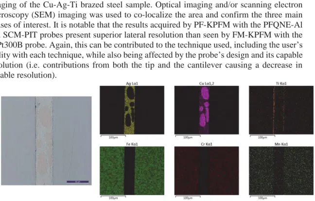
(Cu-Ag-Ti). Elemental mapping of the sample revealed precipitation of copper-rich regions within a eutectic silver-rich matrix, with titanium showing strong properties as a wetting agent by diffusing to the braze-steel interfaces (Figure 3). Figure 4 shows VPD maps using the different probe types, all whose modified work functions were calculated just prior to imaging of the Cu-Ag-Ti brazed steel sample. Optical imaging and/or scanning electron microscopy (SEM) imaging was used to co-localize the area and confirm the three main phases of interest. It is notable that the results acquired by PF-KPFM with the PFQNE-Al and SCM-PIT probes present superior lateral resolution than seen by FM-KPFM with the 25Pt300B probe. Again, this can be contributed to the technique used, including WKHXVHU¶V ability with each technique, while also being affected by the probe¶V design and its capable resolution (i.e. contributions from both the tip and the cantilever causing a decrease in capable resolution).
Figure 3. Co-localized optical and energy dispersive X-ray spectroscopy of Cu-Ag-Ti brazed steel sample, confirming three distinct phases of stainless steel, copper-rich regions, and a silver-rich braze matrix.
Regardless of resolution, it can be seen from Figure 4 that all three maps present consistent relative phase nobility, where the silver matrix is nobler than the copper-rich regions, while steel is seen as a more active region than the brazing phases. Although the relative nobility of the Volta potential difference maps are the same with different probe types, the resulting numerical values for each phase are notably different, as shown in Figure 5(a). The VPD for a single phase ranges ~730 mV between the images. To place into context, if separate studies on this same material type were done with different probes, the resulting range of probable VPD values for each phase would be 3/4 of a volt. For
REVHUYLQJUHODWLYHQRELOLW\WKLVVKRXOGQ¶WEHVXFKDKDUVKUHDOLW\WRDGGUHVV+RZHYHULILW
so desired to document phase work function values, or placing the VPD values of each phase onto a reference scale, then the large range in measured potentials is not ideal.
For this case, Figure 5(b) presents the method of using gold as a reference prior to imaging the Cu-Ag-Ti brazed steel sample. Displayed on the left y-axis is the VPD of each phase relative to the gold of the Al-Si-Au standard. Another way to display the results can be seen on the right y-D[LVZKHUHHDFKSKDVH¶VUHODWLYHZRUNIXQFWLon is calculated directly from equation 1. Again, the gold from the Al-Si-Au standard is used as reference to quantify the relative work function of the operating probe, which in turn is used to calculate the relative work function of each phase on the Cu-Ag-Ti brazed steel sample. From this, the distribution of plausible results for each of the phases has reduced from a maximum spread of ~730 mV (or 0.73 eV) to a spread of ~140 mV (or 0.14 eV).
Figure 4. (a) SEM and SKPFM co-localization on Cu-Ag-Ti brazed steel sample with a PFQNE-Al probe. (b) Optical and SKPFM co-localization on Cu-Ag-Ti brazed steel sample with 25Pt300B probe. (c) SEM and SKPFM co-localization on Cu-Ag-Ti brazed steel sample with SCM-PIT probe.
Figure 5. (a) Average Volta potential difference results for steel, copper, and silver-rich regions of the Cu-Ag-Ti brazed steel sample with (orange square) a PFQNE-Al probe, (blue triangle) a 25Pt300B probe, and (silver circle) a SCM-PIT probe. (b) Normalization of the resulting plot with relative scaling from the gold standard prior to imaging of the Cu-Ag-Ti brazed steel sample.
The same process can also be used for imaging with different probes of the same type. The PFQNE-Al probe provided by Bruker has shown to provide high resolution images, and thus was chosen. Figure 6 presents the Volta potential difference maps for two of three images that were captured by different PFQNE-Al probes on different dates. The third VPD map is presented by Kvryan et al (20). Figure 7(a) displays the VPD of each phase from the three separate images. Again, although the relative nobility is consistent, the three separate tests conducted on this material by probes of the same make-up would present three differing VPD values for each phase. However, using the method outlined in this work, the resulting distribution for each of the phases reduces the average spread from ~650 mV (or 0.65 eV) down to ~110 mV (or 0.11 eV), as seen in Figure 7(b).
Figure 6. SKPFM results of the Cu-Ag-Ti brazed steel sample, with (a) a PFQNE-Al probe and (b) with a different PFQNE-Al probe, as seen in Figure 5(a).
Figure 7. (a) Average Volta potential difference results for steel, copper, and silver-rich regions of the Cu-Ag-Ti brazed steel sample (orange square) as seen in Figure 6, (red diamond) a different PFQNE-Al probe, and (black hollow circle) data results by Kvryan et al. (20). (b) Normalization of the resulting plot with relative scaling from the gold standard prior to imaging of the Cu-Ag-Ti brazed steel sample.
Conclusions
It is standard in a three-electrode electrochemical testing to have results presented with regards to a reference or standard. With this distinction, results from separate sets of experimentation can be comparable on a relative scale. This work presents a similar methodology for SKPFM Volta potential difference results by utilizing a relatively inert reference material. Implementing this simple addition to standard SKPFM practice can reduce the notable distribution in reported Volta potential differences for evident surface phases seen in metallic alloys.
A rescaling methodology was accomplished on a complex microstructure of a 316L stainless steel sample joined by a Cu-Ag-Ti brazing material. Some observable variation is still seen in the results; however, these results lessened the notable gap in VPD results. Also, these results being accumulated over approximately a three year timeframe, as well as acquiring results in atmospheric conditions provides reasonable causes of error in phase VPD and work function.
:KLOH 6.3)0 LV XVHIXO IRU GHWHUPLQLQJ UHODWLYH QRELOLW\ RI D PDWHULDO¶V SKDVH
distribution, it is important to align results onto a similar scaling versus a relatively inert material. Results before this rescaling showed a much greater distribution of phase Volta potentials than seen after the rescaling process was accomplished. This distinction can allow reproducibility of specific materials and their phases with others in the scientific field. Future reproduction of this methodology may choose to utilize other tools, such as X-ray photoelectron spectroscopy, to provide exact work function values for a reference material, and thus improve determining absolute work function mapping of highly resolved microstructures.
This was completed to support bridging the gap between modeling from DFT and experimentation with SKPFM. With this, we can start to provide a quantitative relationship between work function calculations to Volta potential difference measurements. With both
the use of DFT and 6.3)0ZHFDQEHJLQWRFDWDORJPDWHULDOV¶SKDVHGLVWULEXWLRQIRUWKHLU
direction and magnitude of nobility in microgalvanic coupling, and thus have a greater understanding of the driving force of corrosion initiation and progression.
Acknowledgments
Support from the NASA Idaho Space Grant Consortium and U.S. Department of Energy is greatly acknowledged. DFT calculations were performed through the Battelle
consortium with ,GDKR 1DWLRQDO /DERUDWRU\ DQG %RLVH 6WDWH¶V 0DWHULDO 7KHRU\ DQG
Modeling Group. Experimental assistance from the Boise State Surface Science Laboratory (SSL) and the Boise State Center for Materials Characterization (BSCMC) is also acknowledged.
References
1. Nonnenmacher, M. P. Oboyle, and H. K. Wickramasinghe, Appl. Phys. Lett.58 (25), 2921 (1991).
2. J. M. R. Weaver and D. W. Abraham, J. Vac. Sci. Technol. B9 (3), 1559 (1991). 3. M. Rohwerder and F. Turcu, Electrochim. Acta53, 290 (2007).
4. S. Sadewasser, T. Glatzel, S. Schuler, S. Nishiwaki, R. Kaigawa, and M. C. Lux-Steiner,
Thin Solid Films431-432, 257 (2003).
5. F. Krok, K. Sajewicz, J. Konior, M. Goryl, P. Piatkowski, and M. Szymonski, Phys. Rev. B77, 235427 (2008).
6. Y. Leng, C. C. Williams, L. C. Su, and G. B. Stringfellow, Appl. Phys. Lett.66, 1264 (1995).
7. N. J. Lee, J. W. Yoo, Y. J. Choi, C.J. Kang, D. Y. Jeon, D.C. Kim, S. Seo, and H. J. Chung, Appl. Phys. Lett.95, 222107 (2009).
8. H. Hoppe, T. Glatzel, M. Niggemann, A. Hinsch, M. C. Lux-Steiner, and N. S.
Sariciftci, Nano Lett.5, 269 (2005).
9. P. Campestrini, E. P. M. van Westing, H. W. van Rooijen, and J. H. W. de Wit, Corr. Sci.42, 1853 (2000).
10.J. H. W. de Wit, Electrochim. Acta49 (17-18), 2841 (2004).Fandre 11.F. Andreatta, H. Terryn, and J. H. W. de Wit, Corr. Sci.45, 1733 (2003).
12.F. Andreatta, H. Terryn, and J. H. W. de Wit, Electrochim. Acta49, 2851 (2004). 13.C. Larignon, J. Alexis, E. Andrieu, L. Lacroix, G. Odemer, and C. Blanc, Electrochim.
Acta110, 484 (2013).
14.M. Sarvghad-Moghaddam, R. Parvize, A. Davoodi, M. Haddad-Sabzevar, and A.
Imani, Corr. Sci.79, 148 (2014).
15.Y. Jin, M. Liu, C. Zhang, C. Leygraf, L. Wen, and J. Pan, J. Electrochem. Soc.164 (9), C465 (2017).
16.P. Schmutz and G. S. Frankel, J. Electrochem. Soc., 145 (7), 2285 (1998).
17.V. Guillaumin, P. Schmutz, and G. S. Frankel, J. Electrochem. Soc. 148 (5), B163 (2001).
18.A. B. Cook, Z. Barrett, S. B. Lyon, H. N. McMurray, J. Walton, and G. Williams,
Electrochim. Acta66, 100 (2012).
19.M. F. Hurley, C. M. Efaw, P. H. Davis, J. R. Croteau, E. Graugnard, and N. Birbilis,
Corrosion71 (2), 160 (2015).
20.A. Kvryan, K. Livingston, C. M. Efaw, K. Knori, B. J. Jacques, P. H. Davis, D. P. Butt, M. F. Hurley, Metals6, 91 (2016).
21.A. E. Coy, F. Viejo, P. Skeldon, and G. E. Thompson, Corr. Sci.52, 3896 (2010). 22.L. Vieira, F. L. C. Lucas, S. F. Fisssmer, L. C. D. dos Santos, M. Massi, P. M. S. C. M.
Leite, C. A. R. Costa, E. M. Lanzoni, R. S. Pessoa, H. S. Maciel, Surf. Coat. Technol.
260, 205 (2014).
23.C. F. Mallinson, A. Harvey, and J. F. Watts, J. Electrochem. Soc. 164 (7), C342 (2017). 24.P. Schmutz and G. S. Frankel, J. Electrochem. Soc.145 (7), 2295 (1998).
25.K. H. Anantha, C. Örnek, S. Ejnermark, A. Medvedeva, J. Sjöström, and J. Pan, J. Electrochem. Soc. 164 (4), C85 (2017).
26.L. Lacroix, L. Ressier, C. Blanc, and G. Mankowski, J. Electrochem. Soc. 155 (1), C8 (2008).
27.D. Sun, Y. Wang, Y. Lu, and Q. Rao, Superlattices Microstruct.94, 215 (2016). 28.B. S. Tanem, G. Svenningsen, and J. Mardalen, Corros. Sci.47, 1506 (2005).
29.K. A. Yasakau, A. N. Salak, M. L. Zheludkevich, and M. G. S. Ferreira, J. Phys. Chem.
114, 8474 (2010).
30.C. Li, S. Minne, Y. Hu, J. Ma, J. He, H. Mittel, V. Kelly, N. Erina, S. Guo, and T. Mueller, Bruker Corporation, Santa Barbara, CA, USA (2013)
31.P. Leblanc and G. S. Frankel, J. Electrochem. Soc.149 (6), B239 (2002). 32.W. Melitz, J. Shen, A. C. Kummel, and S. Lee, Surf. Sci. Rep.66, 1 (2011). 33.P. Hohenberg and W. Kohn, Phys. Rev. B136, 864 (1964).
34.W. Kohn and L. J. Sham, Phys. Rev.140, A1133 (1965). 35.G. Kresse and J. Furthmüller, Phys. Rev. B54, 11169 (1996). 36.G. Kresse and D. Joubert, Phys. Rev. B59, 1758 (1999).
37.J. P. Perdew, K. Burke, and M. Ernzerhof, Phys. Rev. Lett.77, 3865 (1996). 38.J. P. Perdew and W. Yue, Phys. Rev. B33, 8800 (1986).
39.S. Kajita, T. Nakayama, and J. Yamauchi, J. Phys. Conf. Ser.29, 120 (2006). 40.N. E. Singh-Miller and N. Marzari, Phys. Rev. B80 (23), 235407 (2009). 41.R. M. Eastmen and C. H. B. Mee, J. Phys. F: Met. Phys.3 (9), 1738 (1973). 42.J. K. Grepstad, P. O. Gartland, and B. J. Slagsvold, Surf. Sci.57 (1), 348 (1976).