Analysis on Solar Panel Crack Detection Using Optimization Techniques M.D. Dafny Lydia1,*, K. Sri Sindhu2, K. Gugan3
1 AMET University, Kanathur, Chennai-603112, Tamil Nadu, India 2Prathyusha Engineering College, Chennai-602025, Tamil Nadu, India
3AMET University, Kanathur, Chennai-603112, Tamil Nadu, India
(Received 18 December 2016; revised manuscript received 25 April 2017; published online 28 April 2017) A Solar panel is considered as a proficient power hotspot for the creation of electrical energy for long years. Any deformity on the solar cell panel’s surface will prompt to decreased production of power and loss in the yield. Subsequently, the location of cracks on solar panel surfaces is the most essential stride during the inspection of solar panel, and it has important significance. In any case, these strategies cost lot of computation time and with low precision. Aiming for a few issues of the existing algorithm, a new frame-work is proposed to distinguish the cracks. Crack can be distinguished by utilizing optimization techniques based on segmentation. The optimization techniques are Particle Swarm Optimization (PSO), Differential Particle Swarm Optimization (DPSO) and Fractional Order Differential Particle Swarm Optimization (FODPSO). It is important to identify the crack in solar panel cells since they can directly diminish the ex-ecution of the panel and additionally the power yield. In view of the segmentation process, the potential regions which have cracks have been found, and then distinctive optimization algorithms were run on the-se areas to discover crack pixels. An extensive number of trials demonstrate that, this technique procures high accuracy and more complete crack contours with low computation costs.
Keywords: Solar cell, Particle Swarm Optimization (PSO), Differential Particle Swarm Optimization (DPSO) and Fractional Order Differential Particle Swarm Optimization (FODPSO)
DOI: 10.21272/jnep.9(2).02004 PACS numbers: 01.50.hv, 01.50.Kw
*[email protected] 1. INTRODUCTION
Electrical energy generation has been a basic issue in aircraft and orbital hardware such as satellites. Since energy production is expensive, renewable energy sources like wind, solar energy are widely used as a suitable solution to produce electrical power. As of late, solar energy and photovoltaic (PV) have been considered as a significant electrical energy generation reserve. It can be acquired by converting solar energy to electrical power with highest efficiency and high dependability. The deformities in photovoltaic cell [1] might be because of manufacturing imperfections, misusing the panel, cracks may happen through to sharp objects while in-stallation or might be transportation. Recently some automated crack detection methods that use image pro-cessing have been proposed.
Distinctive sort of solar cell products have been cre-ated with crystalline silicon as the most common kind of mono-crystalline varieties are delivered whereby poly-crystalline solar cells are more connected to produce solar cell panels and are more prominent than mono-crystalline ones. Whether the solar cells depend on sin-gle crystalline or polycrystalline silicon, the most vital component is avoidance of any cracks and imperfections to acquire the product with high quality.
The most common faults in solar panels are con-cerned with cracks which are found on the surface of solar cells which can prompt to loss of yield. In this case, during the assembly and generation processes, it is important to guarantee the obtaining of a good end-product. Sometimes mechanical cracks like micro cracks will happen on cell panels at any circumstance. They can specifically influence efficiency and may decrease
the performance. It is important to distinguish cracks on solar cell panels and thus dismiss flawed products. Numerous techniques have been produced to review the solar cell panels, and these have distinctive strengths and shortcomings. Some assessment frameworks are acoustic microscopy and impact testing, radiometric pulse and thermal imaging, hyper-spectral imaging, defect surface iridescence, resonance ultrasound vibra-tion and image processing approach to deal with the solar cell which was displayed for crack detection in solar cell panels. Still it is essential to locate a produc-tive approach, which will be a contact, non-destructive and low-cost inspection framework.
Q. Li, W. Wang, et al [2] 2010, clarified the execu-tion of an inspecexecu-tion based on image processing ap-proach. They concentrated on crack discovery on the edge and inside the captured image of solar cell panel. They distinguished and grouped the cracks based on the grey value difference of the pixels between a region and its encompassing pixels. Their created framework com-prised of image converting, altering of image, Gauss-Laplacian image transformation, converging of distrib-uted points to get a coordinated region, contour recogni-tion to recognize the cracks which are situated on inside or edge of a solar cell.
G. N. Tiwari et al [3] 2011, presented a framework in view of the image processing approach for defect identification in solar modules. They utilized semicon-ductor electroluminescence devices for capture from solar cell modules. They introduced distinctive types of imperfections and characterized them into black pieces, broken grid, fragmentation, and cracks in the solar cell module. Their system software was composed of gray scale transformation, binary and feature extraction.
They proposed the binary method based on transfor-mation of a feature’s gray value between different re-gions. Their identification method to recognize the crack from a broken grid depends on following the trajectory; a crack is distinguished in terms of the projection ratio of outermost and closest horizontal degree in each solar cell. Their outcomes for acknowledgment rate of deform-ities were introduced as the following: black piece is 99%, broken grid and fragmentation is 95 % and the rate for crack detection is 80 %.
D.M Tsai et al [4] 2010, the author developed an in-vestigation framework based on machine vision for identifying micro cracks on solar cell wafers. Their framework has a quick computational operation of 0.09 s for a 640 480 image.
Fang Shuai et al [5] 2012, has proposed a framework in view of machine vision to recognize undetectable mi-cro cracks in solar cells. To search these out, they set up an IR imaging framework to capture images of interior micro cracks. They applied flaw detection algorithms to extricate micro crack elements of solar cells. Their test result showed a 99.85 % precision of their flaw detection system.
Zou Q et al [6] 2012, introduced a emitting light ma-terial to recognize defects on solar cells in view of the current difference in intensity conveyance of electrolu-minescence (EL). They built up an infrared thermogra-phy strategy for defect recognition in solar cell panels. Their framework comprised of an IR camera in order to capture the image of the solar cell, propagating ther-mals along the surface of the solar cell and edge detec-tion administrator to identify the edge of cracks.
Y.C. Chiou et al [7] 2010, built up a framework us-ing acoustic estimations. It can be precise by excitation of vibratory modes in a solar cell which can identify cracks and their areas. Some non-image processing test-ing techniques are introduced by [1] where a review strategy in view of hyperspectral imaging to recognize cracks in solar cell panels was developed. For laser fil-tering and hyper-spectral imaging, the spectral angle mapper was adopted to perceive the imperfections on solar cell panels.
M. Kontges et al [8] 2011, utilizes digital image pro-cessing to recognize areas in an image by utilizing dif-ferent segmentation methods. This paper gives a brief record on five of the distinctive segmentation proce-dures namely region growing, watershed, thresholding, crack and merge, k-means clustering techniques high-lighting the points of interest and also the hindrances of each of these techniques. A change of traditional region growing segmentation method is presented which con-sequently chooses the seed points and develops the re-gions until all rere-gions in the image are divided. The consequences of segmentation techniques introduced in the paper are not reliant on the type of image to be segmented and these techniques are utilized as a part of segmenting industrial radiographic weld images in which a few defects like porosity, absence of fusion, slag line, inadequate penetrations, and wormholes happen. The techniques are assessed on different types of imag-es and efficiency of thimag-ese techniquimag-es in the detection of a few weld imperfections is presented along with the experimental results.
Y. Nosaka et al [9] 2011, utilizes an arrangement of
solar cells which are collected and interconnected into a large solar module to offer a lot of power for commercial applications. Numerous defects in a solar module can't be outwardly seen with the routine CCD imaging framework. This paper goes for defect inspection of solar modules in electroluminescence (EL) images. The solar module charged with electrical current will radi-ate infrared light whose intensity will be darker for intrinsic crystal grain boundaries and extrinsic defects including micro-cracks, breaks and finger interrup-tions. The EL image can particularly highlight the in-visible defects additionally make an irregular inhomo-geneous background, which makes the examination task troublesome. The proposed strategy depends on Independent Component Analysis (ICA), and includes learning and detection stage. The vast solar module image is initially divided into small solar cell sub imag-es. In the training stage, an arrangement of defect-free solar cell sub images is utilized to find a set of inde-pendent basis images using ICA. In the inspection stage, each solar cell sub image under examination is reconstructed as a linear combination of the learned basis images. The coefficients of the linear combination are utilized as the feature vector for characterization. Likewise, the reconstruction error between the test image and its reproduced image from the ICA basis images is additionally assessed for determining the presence of defects. Test results have shown that the image reconstruction with basis images unmistakably outperforms the ICA feature extraction approach. It can accomplish a mean recognition rate of 93.4 % for a set of 80 test samples.
2. OVERVIEW
In this work, image processing (both visible, near infrared, and far infrared) to examine different parts of solar cells including their materials, device operation, imperfections, variability, and unwavering quality is used. Research center ventures utilizing low-cost fluo-rescent cameras, visible and near-IR cameras and far-infrared thermal cameras are utilized to characterize the grain structure, defects, surface roughness, reflec-tivity, electroluminescence, photoluminescence, and photovoltaic operation of solar cell materials (e.g., mono-crystalline and multi-crystalline silicon wafers), thin-film and nano solar cells, commercial silicon solar cells and photovoltaic modules. The captured image can be import captured images into MATLAB or other broadly accessible image processing software for inves-tigation and translation.
The reason for this work is to create, validate and dissipate a series of solar panel cell modules that use image capture, image processing and image analysis of photovoltaic solar cells to recognize the crack using material science and semiconductor technology includ-ing image based investigations of electrical and optical properties and deformities and image analysis of ele-ments at a few scales (submicron, micron, mm) and in addition packaging, area variability and yield; surface metrology (e.g., micro roughness, cleanliness and sur-face damage, etching uniformity and characteristic geometries of micro structured surfaces); metallog-raphy (microstructure like grain boundaries and
tex-ture, i.e., favored grain orientations and size distribu-tions and their effect on material performance); thin-film optics like anti-reflection coatings; many aspects of photo-voltaics and other optoelectronic devices, for ex-ample, LEDs, sensors; flat panel displays and other energy transformation devices like photo cathodes; basic ideas of hyperspectral and remote imaging; radia-tive, conductive and convective heat exchange and dif-ferent heating and cooling techniques (resistive heating and convective heating /cooling, thermoelectric (Peltier) impacts, optical heating with lasers and flash lamps, ultrasonic heating); thermal and infrared material sci-ence especially identified with thermal imaging and IR optics; Thermomechanical properties of materials, for example, thermal extension and thermal initiated stresses; CCD/CMOS cameras including mobile phone and web cameras, thermal imaging cameras, and visi-ble UV and IR quantum and thermal identifiers; image capture, image handling and image analysis such as edge sharpening and detection, skeletonization, seg-mentation, convolution and filtering, feature and pat-tern registration and recognition, scientific morphology and more advanced techniques; signal processing and signal extraction from noise, for example, actualized with filtering, phase-sensitive detection and lock-in amplification methods; Non-destructive testing includ-ing illustration of subsurface components and imper-fections; robotics (pick and place, sorting, conveyer built examination); machine vision for quality and pro-cess control; reliability, as identified with, for instance, hotspots created by printed circuit panels and solar modules working in the field.
3. SOLAR IMAGING MODULES
Images of solar cells directly demonstrate the mi-crostructure, especially grain boundaries. Unlike met-als, silicon uncovers its grain structure without the requirement for any sample preparation. A significant number of algorithms (including ASTM protocols) used to parameterize microstructure from images are ap-plied. ASTM systems use lineal and areal examination and similar techniques, to determine grain estimate appropriations and grain symmetry (e.g., equi-hacked or elongated) will be executed with MATLAB.
Images of solar cells are examined to identify sur-face consistency and utilize standard image processing to quantify solar cell components, for example, intact or broken network lines, consistency of AR coating and micro-cracks in solar cells. Likewise coat the dry cells with standardized arrangements of particulates to quantitatively survey deformity appropriations and areal yields.
More sophisticated solar cell imaging processing, especially for micro-crack detection has been described by TSAI who used anisotropic diffusion algorithms for crack inspection of textured silicon solar cells, and for improved feature recognition, as well as imaging of laser speckle patterns.
Measure the thermal expansion of solar cell lami-nates using digital image correlation. Electrolumines-cence Imaging of Solar Cells is Similar to PL imaging, but luminescence is excited by electrical bias.
White light interferometry produces images of solar
cells that demonstrate surface texture. The VEECO white light interferometer produces images that can be utilized to evaluate surface roughness. This can be con-trasted with roughness estimations made by different techniques. Intensity histograms examination can be related with roughness measured by a surface stylus profiler, laser light disseminating, interferometry or atomic force microscopy). There are various MATLAB algorithms in the trade and research literature on re-lating parameters extricated from images with rough-ness estimations by non-imaging strategies. Surface roughness can be surveyed by CCD image based strat-egies.
Drops of different fluids (water, electrolyte solutions and organics) on semiconductor surfaces demonstrate trademark wetting edges that showed oxidation, com-pound formation and cleanliness. Wetting angles can be measured precisely with a CCD camera and identi-fied with surface energies.
Image Capture of Solar Cells on a Conveyer Belt with Robotic Sorting is the significance of image cap-ture processing and investigation to make an interpre-tation of the strategies to the factory floor. Here the goal is to decide how segregating and fast image pro-cessing can be done "on the fly". LBIC (Light-Beam Induced Current) studies are the traditional intends to delineate solar cell performance. A robotic arm holding laser pointers (IR, red, green, and blue emission) to scan a solar based cell and create a map of localized current generation which is delicate to deformities such as grain boundaries and shunts is utilized. Current variation is because of blemished regions of the solar cell. This LBIC guide can be compared with lumines-cence images of the cell. Infrared transmissions through the silicon solar cells can be imaged by placing a heated stage behind the solar cell, which goes about as a blackbody source. The free carriers make absorp-tion impacts with the end goal that the transmission thermal image maps the imperfections of the solar cell.
Scanning a Solar Cell Surface with a Laser Light Scatter is a process where the laser light scattering estimation is regularly a point (0.5 mm) measurement. A modified robotic arm to filter the solar cell and map surface roughness of solar cells can be utilized. In Pho-toluminescence (PL) Imaging of Solar Cells the solar cell can be excited with a laser or flash light and (with filtering) the infrared photoluminescence can be im-aged with a CCD camera with silicon or close infrared. In GaAs detector the components are mid-IR MCT in-dicator components.
Fluorescent dyes are retained on the surface of the solar cell and can be expelled by rinsing. Fluorescent imaging, exciting with a UV light and recognizing visi-ble emission reveals the viability of cleaning systems. A DOE (Design Of Experiments) to enhance cleaning is performed. Clean surfaces are significant in numerous technologies including medical devices. The image for review is presently empowered by the late advance-ment of high-power, ultra-broadband "white light" la-ser-like sources (400 nm to 2 micron wavelengths, 6 W control) with coherence and collimation more like la-sers than conventional light sources. These are current-ly accessible from FianiumInc (Eugene, OR and UK) for a few thousand dollars with optical fiber outputs.
Secure thermography is generally a late advance-ment in imaging and can be accomplished for some imaging modalities. Secure procedures demonstrate the utility of quadrature (stage delicate location) and are the guideline of present day MRI and NMR imaging, and are utilized progressively as a part in medical fields, and Non-Destructive thermography in the aero-space, electronics, and automobile industries. Tempera-ture difference sensitives in the 10 micro Kelvin range are practical. Numerous thermal cameras have exter-nal triggering for secure imaging. Secure thermogra-phy permits the thermal waves (and reflections at in-terfaces and deformities) to be imaged in pulse ther-mography strategies, the investigation of which in-volves extremely intriguing transient heat conduction examination and image processing from the point of view of signal recovery and minimization of noise im-pacts.
4. PROPOSED SYSTEM
The crack in solar panel cell has been identified by different optimization algorithms and the crack may be due to manufacturing defects, mishandling etc. It makes sense that for maximum power generation, each solar cell panel must be in good working condition. To give this affirmation, both post production and once the panel is working in the field, the industry is expanding utiliz-ing thermal imagutiliz-ing as its preferred strategy for findutiliz-ing defects.
Thermal imaging permits irregularities to be seen plainly and, unlike other techniques, can be utilized to scan installed solar panels amid normal operation. It is profoundly a time effective process as a substantial region can be examined in minutes. Cooled thermal imaging cameras have been utilized as a part of the innovative work of solar panel technology for a long time however it is the commercial uncooled cameras that are normally satisfying the post-production, quali-ty control and maintenance applications.
4.1 Steps of Software Component
The input image of the solar panel surface has been captured from the camera while running the Matlab code for Particle Swarm Optimization (PSO), Differen-tial Particle Swarm Optimization (DPSO) and Fractional Order Differential Particle Swarm Optimization (FOD-PSO) to recognize the crack which frequently occurs on the edges. For this situation, optimizing of edge detec-tion will be performed on pixels from the captured image as indicated by the path of the connected curves on the image. So, the edges of regions will be recognized.
In this technique, two vital parameters were con-sidered, i.e. homogeneity and uniformity from curves. They were applied to make the objective function for BF edge detection. This technique can likewise be uti-lized as a part of noisy images and there is no compel-ling reason to apply any filter. The mechanism of the edge detection operator depended on encoding the characteristic of the image to an integer value between 0 and 8.These values encoded as a particle depend on the direction of the movement on a curve. Thus any particle is denoted as k1, k2, k3… kn, where ki is an
in-teger value between 0 and 8.
Homogeneity is likeness of homogeneity pixels on a curve and uniformity is the similarity of intensity of pixels along the curve. In this method, measuring ho-mogeneity for Hoho-mogeneity and measuring similarity of intensities for Uniformity of pixels will be consid-ered. Identified edges ought to be removed with the goal that a few features, for example, cracks and bus bars will be perceived.
The sensed image is acquired from an ordinary CCD camera and light source that demonstrates the cracks with low gray levels and high gradients. The diffusion procedure smoothens the presumed defect region and preserves the crystal grain background. The crack area can then be well identified by subtracting the diffused image from the original image. The strate-gy is particularly intended to recognize micro cracks assuming micro-cracks exhibit darker intensity and higher gradient from their surrounding in the CCD-captured image.
The typical CCD image can't identify the invisible internal cracks and the algorithms can just recognize the specific outer micro-cracks in solar wafers [10]. In the existing method the mean-shift algorithm to recog-nize three types of defects like saw-mark, unique mark and fingerprint and contamination in multi-crystalline solar wafers can be identified.
The target defects generally present high variation of gradient directions, while crystal grain edges show more consistent gradient directions. The original dark level wafer image is initially converted into an entropy image, where every pixel characterized in a small neighborhood window is represented by the entropy of gradient direc-tions. The mean-shit smoothing procedure is then per-formed to evacuate remove noise and grain edges in the entropy image. The final edge points remained in the filtered image is identified as defective ones.
4.2 Algorithms Used
1. Particle Swarm Optimization (PSO)
2. Differential Particle Swarm Optimization (DPSO) 3. Fractional Order Differential Particle Swarm
Optimization (FODPSO)
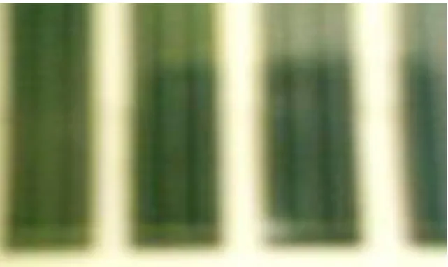
5. METHODOLOGY AND IMPLEMENTATION Using a camera, image is captured as a gray scale format as shown in Fig. 1 and Fig. 2.
Fig. 2 – Input image 2
Segmentation is one of the well known methods used to detect flaws in weldments. Generally the flaws that happen are wormholes, inclusion, lack of fusion, porosity, incomplete penetrations, slag line and cracks. In this paper five types of segmentation techniques which are utilized to identify these flaws are presented. This identification of flaws is utilized in industrial set-ting other than deciding the quality of weldments. The region growing segmentation method gives great results for absence of penetration, cuts and cavity flaws and the watershed segmentation method gives viable results for lack of fusion, slag inclusion and slag lines [11].
Segmentation strategies like region growing, water-shed are used to distinguish flaws in weldments [12]. The consequences of region growing and watershed segmentation techniques are compared [13]. Segmenta-tion normally brings about grouping of adjacent pixels which are similar in some sense. Generally, there are two types of segmentation techniques; one based on discontinuity property of intensities which is referred to as region based segmentation and the other based on similarity property of intensities.
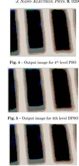
This paper gives an account of region growing, thresholding, watershed, crack and merge and k-means clustering segmentation. Region growing, crack and merge, k-means and watershed segmentation are re-gion based, while thresholding is discontinuity based. The swarm particle concentrates on the number of pix-els which are on a curve, because the best edges exist on curves. It applies for any pixel of an image in order to locate the best curve. In this case, optimizing of edge detection will be performed on pixels from the captured image according to the path of the associated curves on the image. Thus, the edges of regions will be identified. Using MATLAB coding input solar panel image has been captured through Camera. The input image 1 for PSO is shown in Fig. 3. The 4th level output image corresponding to PSO, DPSO and FODPSO is shown in Fig. 4, Fig. 5 and Fig. 6 respectively.
Fig. 3 – Input image 1 for PSO
Fig. 4 – Output image for 4th level PSO
Fig. 5 – Output image for 4th level DPSO
Fig. 6 – Output image for 4th level FODPSO 5.1 Experimental Value for Input Image 1
Three levels (level 2, level 3 and level 4) are per-formed for PSO, DPSO and FODPSO algorithm. The input mean and S.D. is kept constant at 142.97 and 64.81 respectively for all the three algorithms. The output mean and S.D. for PSO 2nd level corresponds to 63.63 and 75.35 respectively. Similarly he output mean and S.D. for PSO 3rd level corresponds to 81.62 and 82.45 respectively. For 4th level the output mean and S.D. are 93.53 and 88.53 respectively.
In case of DPSO, output mean obtained is 63.64 and the S.D. is 75.63. Similarly for 3rd and 4th level of DPSO the output mean and S.D. corresponds to 81.68 and 87.73, 93.43 and 88.68 respectively. For FODPSO, the output mean and S.D. for level 2, level 3, level 4 corresponds to 63.64 and 75.63, 81.55 and 87.69, 93.77 and 88.32 respectively.
5.2 Experimental Value for Input Image 2 The input mean and S.D. for PSO, DPSO and FOD-PSO algorithm for level 2, level 3 and level 4 is main-tained at 86.01 and 48.52 respectively. The output mean and S.D. of level 2, level 3, level 4 for PSO algo-rithm is 21.99 and 45.15, 40.27 and 56.62, 45.57 and 60.06 respectively. Similarly for DPSO algorithm the output mean and S.D. for level 2, level 3, level 4 is 30.00 and 48.68, 40.17 and 56.87, 45.28 and 60.25 re-spectively. For FODPSO algorithm the output mean
and S.D. for level 2, level 3, level 4 is 30.00 and 48.68, 40.19 and 56.79, 45.48 and 60.11 respectively.
6. CONCLUSION
The early discovery of micro-cracks in solar cells is vital in the production of PV modules. This paper fo-cuses on image processing scheme composed of segmen-tation procedures in view of various optimization
algo-rithms. Since solar cell panel is considered as an effi-cient power source for the generation of electrical ener-gy for long years, any defect on the solar cell panel's surface will prompt to reduce the production of power and loss in the yield. The outcomes demonstrate that the segmentation procedures can detect and recognize micro-crack pixels efficiently in the presence of various forms of noise.
REFERENCES
1. M. Köntges, I. Kunze, S. Kajari-Schröder, X. Breitenmoser, B. Bjørneklett, Sol. Energy. Mater. Sol. C. 95, 1131 (2011).
2. Q. Li, W. Wang, C. Ma, Z. Zhu, Opt. Laser Technol. 42
No 6, 1010 (2010).
3. G.N. Tiwari, R.K. Mishra, S. Solanki, Appl. Energ. 88
No 7, 2287 (2011).
4. D.M. Tsai, C.C. Chang, S.M. Chao, Image Vis. Comput.28
No 3, 491 (2010).
5. Fang Shuai, Li Bin, He Xiang-Hao, J. Chinese Comput. Systems33 No 8, 1868 (2012).
6. Q. Zou, Y. Cao, Q. Li, Pattern Recognition Letters33 No 3, 227 (2012).
7. Y.C. Chiou, M.J.Z. Liu, Sensor Rev.31, 10 (2010).
8. M. Kontges, L. Kunze, S. Kajari-Schroder,
X. Breitenmoser, B. Bjorneklett, Sol. Energ. Mater. Sol. C.
95, 1131 (2011).
9. Y. Nosaka, L.A. David, D.S. Gregory, P.W. Gary, Solar Cells and Photocatalysts, in Comprehensive Nanoscience and Technology (Academic Press: Amsterdam: 2008). 10.D.M. Tsai, C.C. Chang, S.M. Chao, Image. Vis. Comput.
28, 491 (2010).
11.Sangita Dubey, Kamal Shah, Int. J. Adv. Eng. Technol.3
No 2, 765 (2012).
12.V.R. Rathod, R.S. Anand, Alaknanda, Proceedings of the 2nd International Conference on Computer and Automa-tion Engineering (ICCAE), 673 (Singapore: 2010).
13.V. Vaithiyanathan, M.M. Raj Anishin, B. Venkataraman, Eur. J. Sci. Res.66 No 3, 449 (2011).