Omar A. C. Vilcanqui1, Antonio C. de C. Lima1 Luiz A. L. de Almeida1,2 Universidade Federal da Bahia (1), Universidade Federal do ABC (2)
Design and Analysis of Amplifiers for Protective Relay Testing
Abstract. This paper presents the analysis and design of voltage and current amplifiers for use in protective relay testing for frequencies up to the 20th harmonic. A typical topology of DC/AC 50/60Hz converters was used to achieve the nominal and peak values produced by conventional current and voltage transformers. The stability analysis is devised considering different requirements of load and frequency response for relay inputs when compared to that of a typical single-frequency power converter. The temporal response to signals with abrupt changes and multiple decaying harmonics is also investigated. Proper test signals are stored in a PC microcomputer and played-back using the analog audio output, which is conditioned to the proposed amplifier input. The amplifier’s controller was implemented using a DSP with PWM and an IGBT H-bridge. Simulations and experimental results are presented for typical faults and multi-harmonic signals.Streszczenie. W artykule zaprezentowano projekt i analize wzmacniacza uzywanego do testowania przeka´zników zabezpieczaj˙ acych w szerokim˛ zakresie czestotliwo´sci, do 20 harmonicznej. Układ umo˛ zliwia tak˙ ze badania przy szybkich zanikach sygnału oraz przy zanikaj˙ acych harmonicznych.˛ Sterownik wzmacniacza wykorzystuje układ DSP z PWM i mostkiem typu H w technologii IGBT.(Projekt i analiza wzmacniacza do testowania przeka´zników zabezpieczajacych)˛
Keywords:Relay Test, Universal Power Supply, Inverter, Protective Relay Słowa kluczowe:przeka´znik, wzmacniacz, testowanie
doi:10.12915/pe.2014.03.25
Introduction
The equipment for testing protective relay currently found on the market is expensive. A relay tester uses current and voltage amplifiers to reproduce compatible signals with the requirements imposed by the relays. This entails the gener-ation of arbitrary signals, usually in the range of DC to the twentieth harmonic with currents and voltages up to 20A and 600V respectively. Procedures for relay testing, which in-clude a dynamic test and transient simulation tests, are pre-sented in [1]. An interesting example found in the literature and intended for use in the educational environment was veloped in [2]. However, such an environment has been de-scribed in a systemic way without the detailed design and analysis of the current and voltage amplifiers. To our knowl-edge, the design and analysis of such amplifiers have not yet been presented in the literature. However, commercial proprietary amplifiers are available, which are also used in RTDS (Real Time Digital Simulator) [3] [4]. A natural choice was to develop the proposed amplifiers using the class D topology that is used in many applications, including power inverters, Universal Power Supply (UPS) [5], programmable power sources [6], voltage and current control sources [7], controllers for multilevel inverters [8], etc. In these applica-tions, the class D amplifier or inverter is used essentially to provide electric power, with afixed-amplitude sinusoidal volt-age source of 50Hz or 60Hz, which does not meet require-ments for testing protective relays.
Linear amplifiers [9] would satisfy these requirements, but the class D topology commonly used in the inverter costs less, is smaller and is more efficient [10]. The signal produced by a traditional inverter, as said before, is sinu-soidal 50/60Hz, and generally this is achieved using a pulse width modulation (PWM) and MOSFET or IGBT switches,
followed by a second order LC filter to remove the
har-monics produced by the switching frequency. These invert-ers are normally subjected to varying loads, which require the use of different classical techniques of control [11] as well as other more advanced techniques such as sliding mode controller [12], Deadbeat [13] and space vector PWM (SVPWM) [14].
To meet the test signal features of a relay test, an al-ternative would be to use a typical Audio Class D amplifier topology [15]. Where in audio applications, the signal
fre-quencies vary between 20Hz to 20kHz, but these amplifiers have voltage and current ratings which limit their usage in relay testing. In addition, the wide bandwidth requires that audio amplifiers operate at high switching frequencies, but without necessarily using feedback on their projects . The requirements for audio amplifiers do not require the use of controllers or switching devices capable of handling high cur-rents and voltages. As a result, the topology of a typical class D audio amplifier is not suitable for use in a relay test.
In this paper, we present the stability analysis of a con-troller to ensure that the class D amplifier meets the require-ments of relay test. This analysis is applied to the topolo-gies for generating the proper currents and voltages ampli-fiers. Simulations and experimental results are presented for typical transient signals of an electric power system, and its reproducibility is validated.
The Topology of Voltage and Current Amplifiers
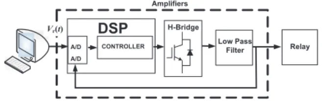
Fig. 1 shows the block diagram of the proposed ampli-fier. The reference signal is generated by a computer and using the audio output it is sent to a digital signal processor (DSP). The analog-to-digital converter of the DSP receives
this reference signalVr(t)to be sampled and used as input
of the amplifier. Unlike a conventional inverter designed to operate at 50/60Hz, the proposed amplifiers must reproduce signals of the type
(1) Vr(t) =
N
n=0
Ane−αntcos(ωnt+φn),
where,An are the amplitudes of the sinusoids,αn the
attenuation factors,ωn andφn the frequencies and phases
of the harmonic components of the reference signal. N is the number of harmonics, including the DC exponential decay
ωn = 0. The reference signal is used to control an H-bridge
composed of IGBT switches, through PWM. To eliminate un-desired harmonic signals from of this modulation, a passive
low-passfilter is used. The cutoff frequency and maximum
fluctuation of current in inductors are of fundamental
impor-tance in the design of thesefilters. The feedback signal for
the controller is obtained at the outputs of the filters. The
current and voltage amplifiers are shown in Fig.2, and have a similar topology to those presented in [16]. In the case of the current amplifier, the low-passfilter is an inductor L. The
DSP
Low Pass Filter Relay CONTROLLER A/D A/D Vr(t) Amplifiers H-BridgeFig. 1. Model of the proposed relay system test.
voltage amplifier has the same structure but with an output LCfilter.
Analysis of Stability Procedure project
The design of passivefilter inductors depends on certain
fac-tors such as the voltage applied on the H-bridge, the size
of the cross-sectional area of the core, theflux density and
the maximum fluctuation of the inductor current, which
de-creases with increasing inductance [17]. This level of
fluctu-ation occurs when the PWM signal is 50%of the duty
cy-cle [16] [17]. In addition, the core material must be able to withstand the involved currents without saturating for the switching frequency [16].
The following equation was used to obtain the
induc-tanceL = VDC/(2fswΔiL), where,fsw is the switching
frequency, VDC is the supply voltage on the H bridge and
ΔiLthe maximumfluctuation of current in the inductor.
S1 S2 S3 S4 R E L A Y L C VDC a b S1 S2 S3 S4 L VDC a b + -+ -Current Filter Voltage Filter H-Bridge
Fig. 2. Model of voltage and current amplifiers for The proposed relay system test in a monofassic configuration.
Open Loop Voltage Analysis
The topology shown at the top part of Fig. 2 was chosen to implement the voltage amplifier. The modulated signal at
the bridge output passes through a low-pass LCfilter. This
filter would lead to instability for high impedance loads be-cause of the resonance peak at the cutoff frequency. In this work, we added a resistance R as Fig. 3 with a low value
compared to the input impedance of the relay Rs. In
com-mon inverter applications, this resonance is attenuated by a very low impedance load. However, the R value is kept as low as possible, but limited to a still high value because of the maximum dissipated power at the output. To reduce the reso-nance peak to a suitable value, while maintaining the R value, we propose the insertion of aRALACAtrapfilter tuned at the
cut-off frequency and a compensation resistorRCin series
with the inductor L, as shown in Fig 3. An important feature of the trapfilter is that its power consumption only occurs at the cutoff frequency, resulting in negligible power amplifier loss.
The transfer function of the voltage across the load
L C Vc(t) Vs is RC iC iL R
Load
Relay Voltage + -RA LA CA VDC RsFig. 3. Proposed Model for the Voltage Amplifier.
impedance and the IGBT bridge output is given by (2)
con-sideringLA =L,CA =C,R RAandRsR. This
last consideration takes into account that commercial relays
may present input impedance values of over hundreds ofkΩ.
(2) Fvc(s) = VVs(s) c(s) = RLCs2+RARCs+R b4s4+b3s3+b2s2+b1s+b0, Where: b4 = RL2C2, b3 = LC(L+RC(RA +RC)), b2 = C(L(3R + RA + RC) + RARCRC), b1=L+C(RC(2R+RA) +RRA),b0=R+RC
The signalVc(t)in Fig. 3 depends on the reference
volt-ageVr(t), the supply voltageVDC and the bridge switching
frequency. A controller must ensure that the amplifier output follows the reference signal with minimum error. The pro-posed controller is designed to act on the H-bridge in order
to obtainflat unit gain in the desired frequency range and a
linear phase corresponding to a small constant time delay. In addition, the amplifier should respond quickly to abrupt tran-sient inputs.
Open Loop Current Analysis
The topology of the current amplifier is shown in Fig. 4. Its outputfilter consists of an inductor L and a burden load
resis-tanceRB corresponds to the input impedance of the relay.
The transfer function relating the IGBT bridge output voltage and the load current is given by.
(3) FiL(s) = iRBV (s) c(s) = 1 LRB, L Vc(t) iRB iL RB
Load
Relay Current+
-VDCFig. 4. Topology of the current outputfilter amplifier.
The analysis of the transfer function described by
equa-tion (3) shows that for commercial burdensRB varying
be-tween0.1−1Ωcauses undesired large variations in
magni-tude and phase response. Thus, it is necessary to insert a current amplifier controller to ensure the desired response.
Closed Loop Voltage Amplifier Analysis
The proposed controller for the voltage amplifier is pre-sented in Fig. 5. It is a parallel combination of the closed loop controllerCv(s)with a feedforward controllerH1(s), this with
large difference between the sampling rate (20kHz) and the maximum signal frequency (1.2kHz) makes the amplifier re-sponse sensitive to the zero order hold (ZOH), which repre-sents the PWM digital-to-analog converter at the DSP out-put. The function that describes the ZOH is the term that multipliesFvc(s)in the equation (6) andFvc(s)is the
math-ematical representation of the low pass filter described by
the equation (2). The computational delay effect described and discussed in [18] [19] [20] is neglected because we use a high-speed DSP with interrupt management at sampling times. H1(s) Cv(s) ZOH + + Fvc(s) + -Vr(t) Controller H-Bridge RELAY
Fig. 5. Block diagram of the of the voltage amplifier controller.
The transfer function of the complete controller, shown in Fig. 5, is given by
(4) Vs(s)
Vr(s) =
Fvc(s)ZOH(s)[H1(s) +Cv(s)]VDC
1 +Cv(s)ZOH(s)Fvc(s) ,
The controller Cv(s) complements the control action of
H1(s), using a block proportional-integral with a cascaded
phase lead compensator, given by
(5) Cv(s) = (10 +120s )(ss+ 2+ 2ππ300003000 ),
The zero-order hold is incorporated into the output analog filter as
(6) Fv(s) = 1−e−T s
sT Fvc(s),
As the controllers are embedded in a DSP, the stability sys-tem analysis has to be carried out in discrete time. Therefore, thefilterFv(s)and the controllerCv(s)are mapped to the Z
domain as expressed by equations (7) and (8) respectively.
(7) Fv(z) =Z[Fv(s)] = (1−z−1)Z[Fvcs(s)],
(8) Cv(z) =Cv(s)|s=2
Tzz−+11,
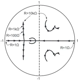
The stability analysis of the proposed system can be performed using traditional techniques such, phase and gain margins analysis and the Roots-Locus method (LGR) [21][22]. In the present work, the stability of the system for different input resistances or loads in the amplifier output must be guaranteed. Thus, we chose the LGR method for our analysis because the other method only allows us to verify if the system is marginally stable. It should be noted that the LGR technique used here does not use the gain variation, as in the traditional method. Alternatively, the open loop gain of the system (4) is regarded as unitary, and the load resistance R varies within a range of interest. Fig. 6 shows the
stabil-ity of system for variations in the load resistance from1Ωto
10kΩ. However, it is important to remember that low
val-ues of load resistances result in excessive and unnecessary power dissipation. Therefore, this limitation should be taken into consideration during the design of the amplifier. Fig. 7 shows the frequency response of the closed-loop voltage am-plifierVs(s)/Vr(s)for a load resistance of10kΩ. The
result-ing response isflat in magnitude in the desired band, with
R=1Ω 1 1 -1 -1 R=10kΩ R=1kΩ R=100Ω R=1Ω
Fig. 6. LGR of the controllerCv(z)Fv(z)with an load resistance R variable in the range of1Ωto10kΩ.
low harmonic distortion in the signal to be amplified. How-ever, this controller does not provide aflat phase response at high frequencies. Despite this, you can playback most typical fault signals of an electrical system without relevant loss for a relay test. -5 0 5 Ma gnitude (dB) 100 101 102 103 104 -225 -180 -135 -90 -45 0 Phase (deg) Bode Diagram Frequency (Hz)
Fig. 7. Frequency response of the closed-loop voltage amplifier for R =10kΩ.
Closed-Loop Current Amplifier Analysis
The current amplifier is designed using a similar proce-dure to that of the voltage amplifier. The modeling of this
amplifier is represented by (9) withFiL(s) provided by the
equation (3).
(9) Fi(s) = 1−e
−T s
s FiL(s),
To ensure aflat magnitude response, with minimal phase lag,
we designed a proportional-integral controller in cascade with a compensator as described in (10).
(10) Ci(s) = (10 + 10000s )(ss+ 2+ 2ππ35003200),
The stability analysis of the current amplifier is made in the discrete domain. Thus,Fi(s)andCi(s)must be mapped to
this domain, as shown in the equations (11) and (12).
(11) Fi(z) =Z[Fi(s)] = (1−z−1)Z[FiLs(s)],
(12) Ci(z) =Ci(s)|s=2
Tzz−+11,
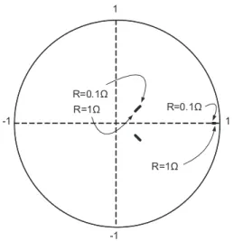
Fig. 8 shows the LGR analysis of the systemCi(z)Fi(z)
for typical relay burden commercial values [3]. It can be ob-served that the stability is maintained for the entire range of load resistance. The closed-loop frequency response for
1 1 -1 -1 R=1Ω R=0.1Ω R=1Ω R=0.1Ω
Fig. 8. LGR of the controllerCi(z)Fi(z)with a load resistenceRB
variable in the range of 0.1 - 1Ω.
RB = 1Ωcan be observed in Fig. 9. In this case, the
mag-nitude isflat with a variation of less than 0.5 dB at a range
of 100Hz to 1.2kHz. The phase response behaves similar to that of the voltage amplifier, with similar implications in the reproduction of fault signals.
-10 -8 -6 -4 -2 0 Magnitude (dB) 100 101 102 103 104 -180 -135 -90 -45 0 Phase (deg) Bode Diagram Frequency (Hz)
Fig. 9. Frequency response of the closed loopCi(z)Fi(z)current amplifier forRBof 1Ω.
Results
Simulation Results
Transient signals representing typical electrical system faults are generated by simulation and played back in an experimental prototype to test the performance of the am-plifiers. These signals contain spectral components as de-scribed in equation (1). Table I shows the component values and parameters used in the simulation and experimental re-sults.
Table 1. Values of Components and Parameters of the Amplifiers
Description Symbol Value
Filter Capacitance C 2.8μF
Filter Inductance Voltage L 1mH
Filter Inductance Current L 500μH
Switching Frequency fsw 20kHz
Network Frequency f0 DC−20aharmonic
Supply voltage VDC 200V
Damping Resistor RD 10Ω
Filter Resistor RA 20Ω
The simulation shown in Fig. 10 illustrates the effect of an overcurrent fault in the feeder voltage, which immediately decreases during the occurrence. The reference signal sent to the voltage amplifier was simulated for a single phase net-work. It can be noted that the controller is capable of repro-ducing the reference (see detail) in less than 1ms. Fig. 11
0 0.02 0.04 0.06 0.08 0.1 0.12 -100 -60 -20 0 20 60 100 Time (s) Amplitude (V) Reference Output 0.054 0.055 -20 -10 0 10
Fig. 10. The reference signal and its corresponding voltage re-sponse at the amplifier output for an overcurrent condition.
shows the simulation of a transient current for a fundamental of 60Hz and an exponentially decaying DC component with a harmonic of 1.2 kHz. The amplifier follows the reference signal introducing a phase delay in the twentieth harmonic, according to the frequency response shown in Fig. 9.
0 0.01 0.02 0.03 0.04 0.05 0.06 0.07 0.08 -2 -1 0 1 2 3 4 5 6 Time (s) Amplitud e (A) Reference Output 1.2 kHz
Fig. 11. Simulation of a transient current signal with exponentially decaying DC component and increasing harmonic of 1.2 kHz.
Experimental Results
The experimental prototype is shown in Fig. 12. It is uses an IGBT H-bridge three-phase model IRAMX20UP60A, which supports maximum voltages of 600V and currents up to 20A. The maximum switching frequency of the bridge is 20kHz and this is used as the sampling frequency of the
con-trol algorithm. The LC filter is built with a ferrite core and
multi-wire winding, and it responds to the twentieth harmonic with negligible losses. The current sensor used is the LEM LA55P and the voltage sensor is the LV20-P. The digital con-trollers are embedded in a Texas DSP TMS320F28335. The program MATLAB is used to generate electrical faults and the analog audio output of the computer is used to generate the references, this output is conditioned to the proposed class D amplifier input. Figs. 13 and 14 show the experimental
re-Fig. 12. Experimental prototype.
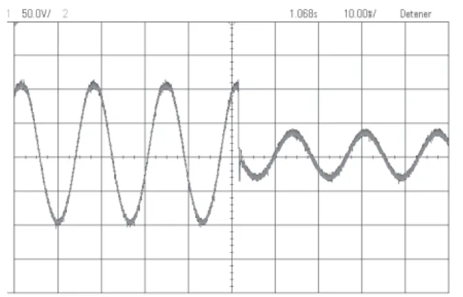
sults corresponding to the simulation presented in Figs. 10 and 11, respectively.
Fig. 13. Experimental result voltage response at the amplifier output for an overcurrent condition.
Fig. 14. Experimental result of a transient current signal with ex-ponentially decaying DC component and increasing harmonic of 1.2 kHz.
Conclusion
The design of current and voltage amplifiers for use in protective relay test has been described. The analysis of a feedback stability of the amplifiers was presented describing curves for load variations where the amplifiers can be un-stable. The control method used to guarantee the stability analysis was the root locus, where the entire amplifier model were mapped in the Z domain. In addition, the procedure to calculate the passive elements of the power amplifiers such
as inductance and capacitance of the filter was described.
A frequency analysis of these amplifiers was performed to
ensure a flat magnitude response and minimal phase
de-lay. The amplifiers were simulated and tested experimentally for some types of transient signals, composed of harmonics, abrupt changes and exponential decays. The good perfor-mance obtained in simulation was verified experimentally, in both frequency and time domain. The results show that the proposed amplifiers may be used for relay testing in the range of DC to 1.2 kHz.
REFERENCES
[1] De Oliveira W. A., Sato F.: A Evolução nos Procedimentos para os Ensaios de Desempenho de Relés de Proteção, In-ternational Conference on Industry Applications 9th IEEE/IAS, INDUSCON 2010.
[2] Pires V.F., Martins S., Amaral T.G., Rodrigues R., Crisostomo M.M.: Distance-Learning Power-System Protection Based on Testing Protective Relays, IEEE Transactions on Industrial Electronics, 55(6), June 2002.
[3] OMICRON, Relay Test [web page] Relay test, http://www.omicron.at/en/products/app/power-system-protection/protection-relays/. [Accessed on 31 Sep. 2013.]. [4] Yoon J.-Y., Kim J.-H.,Yang B., Lee B.: Protective Relay Tests
of Hybrid SFCLs in a Korean Distribution Power System Us-ing RTDS, IEEE Transactions on Applied Superconductivity, 34(5), Jun. 2011.
[5] Abdel-Rahim N. M., Quaicoe J. E.: Analysis and design
of a multiple feedback loop control strategy for single-phase voltage-source UPS inverters, IEEE Transactions on Power Electronics, 11(4), pp. 532-541, Jul. 1996.
[6] Tzou Y.-Y. , Ou R.-S., Jung S.-L., Chang M.-Y.: High-Performance Programmable AC Power Source with Low Har-monic Distortion Using DSP-Based Repetitive Control Tech-nique, IEEE Transactions on Power Electronics, 12(4), Jul. 1997.
[7] Wei Li Y.: Control and Resonance Damping of Voltage-Source and Current-Source Converters With LC Filters, IEEE Trans-actions on Industrial Electronics, 56(5), May. 2009.
[8] Zhang X., Spencer J. W. : Study of Multisampled Multilevel Inverters to Improve Control Performance, IEEE Transactions on Power Electronic, 27(11), Nov. 2012.
[9] Schultz M. A. : Linear Amplifiers, Proceedings of the IRE, pp. 475-485, 1950.
[10] Zhongwei G., Kurokawa F.: Control and PWM Modulation Scheme for Dead-Time Compensation of CVCF Inverters, Telecommunications Energy Conference, INTELEC 2009. [11] Manning C. D.: Control of ups inverters, IEE Colloquium on
Uninterruptible Power Supplies, pp. 3/1-3/5, February 1994. [12] Jung S.-L., Tzou Y.-Y.: Discrete Sliding-Mode Control of a
PWM Inverter for Sinusoidal Output Waveform Synthesis with Optimal sliding Curve, IEEE Transactions on Power Electron-ics, pp. 567 - 577., July 1996.
[13] Kawamura A. , Haneyoshi T. , Hoft R. G. : Deadbeat controlled PWM inverter with parameter estimation using only voltage sensor, IEEE Transactions on Power Eletronics, 33(2), April 1988.
[14] Jacobina C. B., Nogueira L. A. M., Da Silva E. R. C., Alves R. N. C., Seixas P. F.: Digital Scalar Pulse-Width Modulation: A Simple Approach to Introduce Non-Sinusoidal Modulating Waveforms, IEEE Transactions on Power Electronics, 16(3), May 2001.
[15] Adduci P., Botti E., Dallago E., Venchi G.: PWM Power Au-dio Amplifier With Voltage/Current Mixed Feedback for High-Efficiency Speakers, IEEE Transactions on Industrial Elec-tronics, 54(2), pp. 1141-1149, April 2007.
[16] Mohan AN., Undeland T. M., Robbins W. P.: Power Electronics Converters, Applications, and Design, New York: Wiley, 2003. [17] Asiminoaei L., Aeloiza E., Enjeti P. N. Blaabjerg F.: Shunt Active-Power-Filter Topology Based on Parallel Interleaved In-verters, IEEE Transactions On Industrial Electronics, 55(3), pp. 1175-1189, March 2008.
[18] Espi H.M. , Castello M.J., Fischer J.R., Garcia-G. R.: A Syn-chronous Reference Frame Robust Predictive Current Control for Three-Phase Grid-Connected Inverters, IEEE Transactions on Industrial Electronics, 57, pp.954 - 962, March 2010. [19] Yepes A. G. , Freijedo F. D., López Ó., Gandoy J. D. :
Anal-ysis and Design of Resonant Current Controllers for Voltage-Source Converters by Means of Nyquist Diagrams and Sensi-tivity Function, IEEE Transaction On Industrial Electronics, 58, pp. 5231-5250, November 2011.
[20] Yin J., Duan S., Liu B.: Stability Analysis of Grid-Connected Inverter With LCL Filter Adopting a Digital Single-Loop Con-troller With Inherent Damping Characteristic, IEEE Transac-tions on Industrial Informatics, 9, pp. 1104-1112, May 2013. [21] Abusara M.A., Sharkh S.M.: Design and Control of a
Grid-Connected Interleaved Inverter, IEEE Transactions on Power Electronics, 28, pp. 748 - 764. February 2013.
[22] Ito Y., Kawauchi S.: Microprocessor-Based Robust Digital Control for UPS with Three-phase PWM Inverter, IEEE Trans-actions on Power Electronics, 10(2), March 1995.
Authors: Omar Vilcanqui, Universidade Federal da Bahia, Department of Industrial Engineering, Rua Aris-tidis Novis Nro. 2, 40210-630, Salvador-BA-Brazil, E-mail: [email protected].
Antonio Cezar de Castro Lima, Universidade Federal da Bahia, Department of Electrical Engineering, Rua Aris-tidis Novis Nro. 2, 40210-630, Salvador-BA-Brazil, E-mail: [email protected].
Luiz Alberto Luz de Almeida, Universidade Federal do ABC, Department of Instrumentation, Automation and Robotics, Av. dos Estados 5001. Santo André - SP-Brazil, Bairro Bangu, 09210-580, E-mail: [email protected].