A MATCHED FILTER AND COHERENT DIGITIZER FOR PULSED DOPPLER RADAR SYSTEMS
A Dissertation by
JOHN STEVEN MINCEY
Submitted to the Office of Graduate and Professional Studies of Texas A&M University
in partial fulfillment of the requirements for the degree of DOCTOR OF PHILOSOPHY
Chair of Committee, Jose Silva-Martinez Committee Members, Sebastian Hoyos
Sunil Khatri Guergana Petrova Head of Department, Miroslav Begovic
August 2016
Major Subject: Electrical Engineering
ABSTRACT
In this dissertation, a matched filter and coherent digitizer will be presented for pulsed Doppler radar systems. The matched filter is used to filter as much out-of-band thermal noise in the received signal as possible while maintaining pulse shape integrity for various transmitted pulse widths. The coherent digitizer is used to digitize the filtered pulse and recover the Doppler frequency tone, which is often buried in noise and in the presence of large blockers.
A configurable bandwidth filter is presented to be used as a matched filter in a pulsed Doppler radar system. To eliminated dispersion effects in the received waveform, a finite impulse response (FIR) topology is proposed which has a measured standard deviation of in-band group delay of 11.0 ns that is primarily dominated by the inherent delay introduced by the sample-and-hold. The filter is designed to operate at an intermediate frequency (IF) of 40 MHz while being tunable in bandwidth from 3 to 30 MHz, making it optimal for radar systems with varying pulse widths. Employing a total of 128 taps, the FIR filter provides greater than 50 dB sharp attenuation in the stop-band in order to minimize all out-of-band noise in the low SNR received radar signal.
Due to the FIR filter being discrete-time in nature, an anti-alias filter must be used to avoid out-of-band frequency components folding back in-band after sam-pling. A continuous-time filter based on current-reuse differential difference ampli-fiers, which is used as an anti-alias filter, will be presented. The two differential pairs in the differential difference amplifier process two independent input signals but share the same output and bias current. To demonstrate the achievable power savings, a 6th order lowpass Butterworth filter was designed, achieving a 65-MHz
-3-dB frequency, an in-band input-referred third-order intercept point of 12.0 dBm, and an input referred noise density of 40 nV/Hz1/2, while only consuming 8.07 mW from a 1.8 V supply.
Following the matched filter is a coherent subsampling digitizer. Prior to trans-mission, the radar system modulates the RF pulse with a known pseudorandom BPSK sequence. Upon reception, the radar digitizer uses a programmable sample-and-hold circuit to multiply the received waveform by a properly time-delayed version of the known BPSK sequence. This operation demodulates the desired echo signal while suppressing the spectrum of all in-band non-correlated interferers, making them appear as noise in the frequency domain. The resulting demodulated narrow-band Doppler waveform is then subsampled at the IF frequency by a ∆Σ modulator. Be-cause the digitization bandwidth within the ∆Σ feedback loop is much less than the input bandwidth to the digitizer, the thermal noise outside of the Doppler bandwidth can be effectively filtered prior to quantization, providing an increase in SNR at the digitizer’s output compared to the input SNR.
In this demonstration, a ∆Σ correlation digitizer is fabricated in a 0.18 µm CMOS. The digitizer has a power consumption of 1.12 mW with an IIP3 of 7.5 dBm. The digitizer is able to recover Doppler tones in the presence of blockers up to 40 dBm greater than the Doppler tone.
DEDICATION
ACKNOWLEDGEMENTS
As I near the end of my graduate school career, I would like to take a moment to look back and thank the many people who have helped me along the way. Without their patience and understanding, I would not have made it to this final stage.
I would first like to thank my advisor Dr. Jose Silva-Martinez who has been the greatest source of inspiration and assistance to me these years. Our many hours of discussions always left me feeling confident in my work even on the most discouraging of days. His knowledge in analog circuit design and troubleshooting is revered and has inspired me to always keep learning and pushing myself.
I would like to thank Dr. Aydin Karsilayan, Dr. Christopher Rodenbeck, Dr. Michael Elsbury, and Garth Kraus for all of the meaningful discussion and feedback regarding the filter and receiver designs discussed in this dissertation. Their com-mentary is extremely appreciated, and I thank them for all of their feedback on the early drafts of my papers.
I would like to thank all of the students of the Analog and Mixed Signal Center with whom I have had meaningful discussions or worked with including Rida Assad, Marvin Onabajo, Negar Rashidi, Eric Su, Carlos Briseno, and Hongbo Chen.
I would like to thank my committee members – Dr. Sebastian Hoyos, Dr. Sunil Khatri, and Dr. Guergana Petrova – for agreeing to provide their time by serving on my committee.
I would like to thank my parents Mark and Susan Mincey for always being portive of my decisions regarding my education and always providing love and sup-port at all times.
this time of uncertainty in our lives. I am greatful for her never ending love and ecouragement she has shown me.
NOMENCLATURE
∆Σ Delta Sigma
AC Alternating Current
ADC Analog-to-Digital Converter BAW Bulk Acoustic Wave
BPSK Binary Phase Shift Keying CDP Conventional Differential Pair CMFB Common-Mode Feedback
CMOS Complementary Metal Oxide Semiconductor DAC Digital-to-Analog Converter
DC Direct Current
DDA Differential Difference Amplifier DSP Digital Signal Processor
DUT Device Under Test FFT Fast Fourier Transform FIR Finite Impulse Response FoM Figure of Merit
GBW Gain-Bandwidth Product
HD3 Third Order Harmonic Distortion IF Intermediate Frequency
IIP3 Third Order Intercept Point LFM Linear Frequency Modulated MUX Multiplexer
NTF Noise Transfer Function OSR Oversampling Ratio
OTA Operational Transconductance Amplifier PE Power Efficiency
PVT Process, Voltage, and Temperature RF Radio Frequency
SAW Surface Acoustic Wave
SNDR Signal-to-Noise-and-Distortion Ratio SNR Signal-to-Noise Ratio
SOI Silcon-on-Insulator
SQNR Signal-to-Quantization-Noise Ratio STF Signal Transfer Function
TABLE OF CONTENTS Page ABSTRACT . . . ii DEDICATION . . . iv ACKNOWLEDGEMENTS . . . v NOMENCLATURE . . . vii TABLE OF CONTENTS . . . ix LIST OF FIGURES . . . xi
LIST OF TABLES . . . xvi
1. INTRODUCTION . . . 1
1.1 Radar Basics . . . 2
1.2 A Pulsed-Doppler Radar System . . . 3
1.3 Organization of This Dissertation . . . 6
2. LOW-POWER GM-C FILTER EMPLOYING CURRENT-REUSE DIF-FERENTIAL DIFFERENCE AMPLIFIERS . . . 8
2.1 Anti-Alias Filter Requirements . . . 8
2.2 Filter Architecture Selection . . . 10
2.3 Continuous-Time Filters Employing Differential-Difference Amplifiers 11 2.4 Current Reused Gm Cells for Biquadratic Filters . . . 13
2.5 DDA Based Biquad Filter Circuit Implementation . . . 17
2.5.1 Power Efficiency . . . 19
2.5.2 Noise . . . 20
2.5.3 Common-Mode Feedback . . . 23
2.6 Measurement Results . . . 28
2.7 Conclusion . . . 32
3. A 128-TAP HIGHLY TUNABLE CMOS IF MATCHED FILTER FOR PULSED RADAR APPLICATIONS . . . 33
3.2 Circuit Design . . . 44
3.2.1 Sample-and-Hold . . . 44
3.2.2 Tunable Transconductor Cell . . . 52
3.2.3 Active Multiplexer . . . 59
3.2.4 34-Phase Non-Overlapping Clock Generator . . . 61
3.2.5 Switch Design . . . 66
3.3 Measurement Results . . . 67
3.3.1 Fixed Tuning Control Switches . . . 77
3.4 Conclusions . . . 77
4. A BLOCKER-TOLERANT, HIGH-SENSITIVITY ∆Σ CORRELATION DIGITIZER FOR RADAR AND COHERENT RECEIVER APPLICA-TIONS . . . 80
4.1 Subsampling Coherent Digitizers . . . 81
4.2 Proposed Coherent Receiver Design . . . 84
4.3 Circuit Implementation . . . 93
4.4 Measurement Results . . . 98
4.5 Conclusion . . . 106
5. CONCLUSION . . . 109
LIST OF FIGURES
FIGURE Page
1.1 A simple radar example. . . 1 1.2 Block diagram of a pulsed-Doppler radar system with monobit
sub-sampling. . . 4 2.1 FIR filter main spectrum and first image which will alias back in-band. 9 2.2 Ideal magnitude response of 6th order Butterworth filter. . . 10 2.3 Single-stage differential difference amplifier. . . 12 2.4 Typical implementation of a Gm-C biquad filter. . . 14 2.5 (a) Conventional differential pair, (b) dual differential pair using half
the bias current, and (c) current-reuse differential difference amplifier. 15 2.6 Transistor level implementation of proposed current-reused Gm-C
bi-quad. . . 18 2.7 Noise sources for a single transconductor in the proposed DDA topology. 21 2.8 Input referred noise spectral density for anti-alias filter. . . 22 2.9 Classical CMFB topology which loads the amplifier output causing a
reduction in gain. . . 23 2.10 (a) Proposed common-mode feedback circuit with (b) replica circuit
for proper generation of common-mode voltage referenceVCM. . . 24
2.11 Small signal model of mode loop for one of the two common-mode loops. . . 25 2.12 Pole-zero plot for the CMFB loop when the circuit is (a)
uncompen-sated and (b) compenuncompen-sated. . . 25 2.13 Microphotograph of the fabricated low-power Gm-C filter. . . 29 2.14 Magnitude response of the Gm-C filter. . . 30
2.15 In-band group delay of the Gm-C filter. . . 30
2.16 Linearity measurement for the Gm-C filter. . . 31
3.1 Matched filter example with 100 ns pulse time. Top waveform is the input. The second waveform is a filter with 3 MHz bandwidth which is too small for the pulse. The second waveform is the matched filter bandwidth of 10 MHz. The bottom waveform is a 30 MHz bandwidth filter which is excessive. . . 34
3.2 Proposed 128-tap programmable FIR bandpass filter block diagram including time-interleaved sample-and-hold followed by four 32-tap FIR filters with controllable bandwidth. . . 37
3.3 Single-tap implementation illustrating a) system level which includes 32 tunable transconductor cells, charge accumulation capacitor, and switches with b) 34 non-overlapping clock phases. . . 40
3.4 The 32-tap FIR filter architecture system level which includes 32 tun-able transconductor cells, 34 capacitors, switches, and a multiplexer. The clock phases used are illustrated in Figure 3.3b. . . 41
3.5 Magnitude response of FIR filter transfer functions for 3 (blue), 10 (red), and 30 (green) MHz bandwidths. . . 42
3.6 Magnitude responses of ideal filter (blue) and with 20 percent mis-match in filter coefficients (red). (a) 3 MHz bandwidth, (b) 10 MHz bandwidth, and (c) 30 MHz bandwidth. . . 43
3.7 Time-interleaved sample-and-hold architecture. . . 44
3.8 Sample-and-hold amplifier system level. . . 46
3.9 Sample-and-hold amplifier implementation. . . 47
3.10 Sample-and-hold amplifier bias voltage generation. . . 47
3.11 Sample-and-hold amplifier CMFB circuitry. . . 49
3.12 Sample-and-hold amplifier frequency response. . . 50
3.13 Sample-and-hold amplifier input referred noise spectral density. . . . 50
3.14 Sample-and-hold transient. Input signal shown in blue with sample-and-hold output in red. . . 51
3.15 Matlab plot illustrating the filter tolerance to setting the smallest transconductances to 0. The 8 MHz bandwidth case is plotted. The blue waveform is the ideal transfer function. The red waveform shows the magnitude response when gm cells less than 0.1 µA/V are set to
0. The green waveform includes 20 percent random mismatch in the
coefficients. . . 53
3.16 (a) Tunable transconductance topology with polarity control and (b) replica circuit for tuning voltage reference generation. . . 56
3.17 How the current splits in the tunable transconductors. . . 56
3.18 Tunability of 20–90µA/V transconductor. Five control bits were used to access values across the desired range. . . 59
3.19 Time-interleaved MUX topology. . . 60
3.20 17-stage injection locked ring oscillator used for the generation of the 34 non-overlapping clock phases. . . 62
3.21 Clock signals used in the generation of the 34 non-overlapping clock phases. . . 63
3.22 Generation of the non-overlapping clock phases. . . 63
3.23 Input and output of ring oscillator. . . 64
3.24 34 non-overlapping clock phase generator output. . . 64
3.25 Simulation of clock generator showing non-overlapping time. . . 65
3.26 Switch resistance curve vs. input voltage. . . 66
3.27 Microphotograph of the 2mm × 3mm FIR filter chip with 1.6mm × 2.1mm active area. . . 67
3.28 Measured magnitude response of FIR filter at 40 MHz IF. (a) 3 MHz bandwidth and (b) 8 MHz bandwidth. . . 69
3.29 Pull down switch that is missing leaving tuning transistor gates float-ing when they should be pulled to ground. . . 70
3.30 (a) Measured magnitude response of FIR filter. Bandwidths of 1.5, 7.5, and 15 MHz are shown. (b) Measured magnitude response after being compensated for the sinc distortion that appears in (a) due to the missing pull-down switch in the tuning transistors. . . 71 3.31 Measured IIP3 across all filter bandwidths. . . 72 3.32 Total integrated ouput noise power for each bandwidth selection. . . . 73 3.33 Zero crossing based delay detection varies when initial phase is changed. 74 3.34 Mean pulse delay averaged over the filter bandwidth with the
stan-dard deviation illustrated as well. These results include the variations introduced due to the SH. . . 75 3.35 Magnitude response when the tuning control switches are fixed. 3
MHz, 10 MHz, and 25 MHz bandwidths are shown. The red waveforms show the corrected frequency response while the blue ones show what was actually fabricated and tested. . . 79 4.1 Block diagram of a pulsed-Doppler radar system with monobit
sub-sampling. . . 82 4.2 Digitization methods including (a) monobit subsampling, (b) delta
modulation, and (c) the proposed ∆Σ correlation digitizer. . . 83 4.3 Block diagram of proposed receiver. . . 84 4.4 Implementation of proposed coherent digitizer. . . 87 4.5 Simulated FFT of the digitizer output with a first order ∆Σ modulator
with a 40.004 MHz BPSK modulated input. . . 91 4.6 Subsampling process in the frequency domain. (a) Subsampling of
the filtered IF signal, (b) effect of noise aliasing at baseband, and (c) out-of-band noise being filtered by the DSP. . . 92 4.7 Output SNR vs Input SNR for case of 20 kHz Doppler bandwidth,
sampled at 1 MHz, with a matched filter bandwidth of 10 MHz. . . . 93 4.8 Schematic of amplifier used in ∆Σ integrator. . . 94 4.9 Loop gain response of the OTA (a) without the additional filtering
4.10 Input referred noise spectral density of the OTA. . . 96 4.11 Schematic of comparator used with SR latch used to hold the output
bit when the comparator is being reset. . . 97 4.12 Microphotograph of fabricated chip. . . 98 4.13 Measurement setup used to characterize the operation of the digitizer. 99 4.14 Downconverted output of the digitizer for -15 dBm input. (a)
Time-domain waveform showing the pulse width modulated output that is typical of ∆Σ modulators, and (b) the normalized output spectrum showing the noise shaping behavior. . . 100 4.15 Linearity measurement for the digitizer. Fundamental and IM3
com-ponents are plotted. . . 101 4.16 In-band blocker tolerance demonstration. (a) Input spectrum with
-45 dBm signal BPSK modulated with a -15 dBm blocker tone near fIF+fD and (b) the baseband output spectrum showing the recovered
Doppler tone with the blocker suppressed and appearing as noise. . . 103 4.17 Noise floor increases with blocker power linearly. . . 104 4.18 In-band SNR when sweeping blocker power. Input power is fixed at
-45 dBm. . . 104 4.19 The red top waveform is the -10 dB SNR input spectrum. The blue
bottom waveform shows the input spectrum without noise added. . . 105 4.20 Digitized output spectrum when input SNR is -19 dB. SNR at the
output is approximately -12 dB when noise is integrated up to 20 kHz. 106 4.21 In-band SQNR when no blockers are present. Input power is relative
LIST OF TABLES
TABLE Page
2.1 ω0 and Q values for anti-alias filter. . . 10
2.2 Performance comparison between the conventional differential pair, dual differential pair, and proposed current reuse topology. . . 16
2.3 Biquad filter transistor sizes. . . 19
2.4 Biquad filter source degeneration resistor values. . . 20
2.5 Biquad filter CMFB transistor sizes. . . 28
2.6 Comparison to previously published results. . . 31
3.1 FIR filter coefficients to meet the desired filter bandwidths. . . 38
3.2 Transistor dimensions for OTA of Figure 3.9. . . 48
3.3 Transistor dimensions for bias circuitry of Figure 3.10. . . 48
3.4 Transistor dimensions for CMFB circuitry of Figure 3.11. . . 48
3.5 Transconductance values needed to implement FIR filter coefficients for the desired filter bandwidths. Listed Gm values are in µA/V. . . . 54
3.6 Device sizes for the 20 – 90µA/V transconductance cell. All transistor sizes are in µm. . . 58
3.7 Performance metrics of the 20–90 µA/V transconductance cell. . . 60
3.8 Summary and comparison of previous publications. . . 76
4.1 Transistor dimensions for OTA of Figure 4.8. . . 96
4.2 Transistor dimensions for comparator of Figure 4.11. . . 97
1. INTRODUCTION
In the early years of the 20th century, scientists experimented with detecting electromagnetic waves that have been reflected off of objects beginning a new field of research which would become known as radar. In the 1930s just prior to World War II, much development of radars was done for target detection and range deter-mination. In fact, this is where radar gets its name, radio detectionandranging [1]. Figure 1.1 shows a basic example of a radar. The radar transmits an electromagnetic wave toward a target. The target reflects the wave back toward the antenna where it will be captured and analyzed by the system.
Modern radars have evolved from systems that just detect targets and determine their range to systems which identify, image, and classify targets as well. They are able to suppress unwanted interference such as echoes from the environment, known as clutter, and countermeasures, known as jamming.
Tran sm itted – f ref Ech o – fref ± fDop pler
1.1 Radar Basics
A radar is an electrical system that transmits RF electromagnetic waves toward a region of space and receives and detects those electromagnetic waves when reflected from objects in that region [2]. Radars can be divided into two general classes: continuous-wave and pulsed. In a continuous wave radar two antennas must be used – one for the transmitter and one for the receiver. Since isolation between the two antennas is not perfect, there will always be leakage from the transmitter antenna to the receiver antenna. Because of this, continuous-wave radar is generally limited to lower power designs limiting them to short range applications. In order to determine range to an object, the characteristics of the transmitted waveform cannot be constant; often the frequency of the transmitted waveform is varied with some modulation scheme as linear frequency modulation (LFM – a frequency chirp) which essentially creates a timing mark [2].
In a pulsed radar, the electromagnetic waves are transmitted during a short pulse, generally in the range of 0.1 to 10 µs but can be as short as a few nanoseconds or in the millisecond range. Pulsed radars have two major benefits: 1) only one antenna is needed since the receiver can be used during the transmitter’s off-phase, and 2) the receiver can be turned off completely during transmission allowing complete isolation between transmitter and receiver. This allows pulsed radars to operate at much higher power and ranges than their continuous-wave counterparts [2].
Received waveforms always return with some interference which come in four classifications: 1) In all cases, the received waveform will be in the presence of electronic noise that is present in the environment as well as the electronics used in the transmitter and receiver. 2) Often there will be objects not of interest that cause unwanted reflections back to the receiver that are known as clutter. 3) In today’s
world of wireless technology, the atmosphere is filled with electromagnetic radiation from human-made sources which can cause unwanted electromagnetic interference. 4) In military applications, intentional jamming in the form of noise or false targets due to electronic countermeasures is often present. Radar receivers need to be able to perform in the presence of each of these types of interference [2].
The circuits discussed in this dissertation deal with determing two measurements from the received radar pulse – target range and velocity. Because radar uses elec-tromagnetic waves that travel at the speed light, the range R to an object can be determined by
R= c×∆T
2 (1.1)
wherecis the speed of light which is approximately 3×10⁸ m/s and ∆T is the delay between transmission and reception.
When an electromagnetic wave reflects off of a moving object, it will undergo a shift in frequency propertional to the target’s velocity known as a Doppler shift. The Doppler shift can be calculated to be
fD ∼=
2×v
λ (1.2)
where v is the target’s velocity and λ is the wavelength of the transmitted electro-magnetic waveform.
1.2 A Pulsed-Doppler Radar System
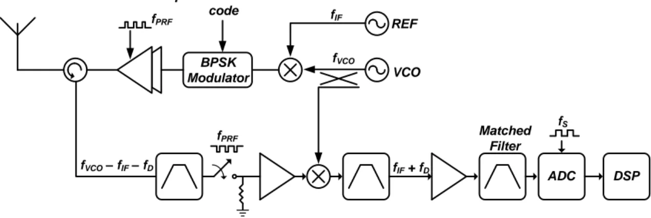
In a pulsed-Doppler radar system, radio frequency (RF) pulses are transmitted, and the Doppler shifted echo signal is returned and processed by the receiver. An example of a pulsed-Doppler radar system [3] is shown in Figure 1.2. This system aims to measure the range and velocity of a target by detecting the transmit time
and Doppler shift of a reflected RF modulated pulse.
fVCO – fIF – fD fIF + fD
Matched Filter ADC DSP fS fPRF BPSK Modulator pseudo-random code fPRF VCO REF fVCO fIF
Figure 1.2: Block diagram of a pulsed-Doppler radar system with monobit subsam-pling.
The transmitter path of Figure 1.2 consists of a pair of signal sources – a reference oscillator operating at the intermediate frequency (IF) fIF and a voltage-controlled
oscillator (VCO) operating at the RF frequency fV CO. The reference signal is
up-converted to fV CO−fIF and then pulse modulated at a pulse repetition frequency
(PRF) fP RF. A pseudorandom Binary Phase Shift Keying (BPSK) phase code of
either 0◦ or 180◦ is employed to eliminate any range ambiguities that may be present while also reducing the receiver sensitivity to any in-band interferers that may be present. The BPSK modulated, pulsed, RF signal is radiated from the antenna to the target and then reflected back to the antenna with some delay proportionate to the distance between antenna and target. The return signal also undergoes a Doppler shift fD dependent on the target’s velocity. The received signal at fV CO−fIF −fD
is amplified, bandpass filtered, and then down-converted by an image-reject mixer to fIF +fD. This IF signal is bandpass filtered through a radar matched filter and
then sampled once per pulse by a 1-bit ADC clocked at fS = fP RF. The sampled
signal is then processed by a digital signal processor (DSP) for analysis to determine the range and velocity of the target.
In these systems, the received signals are typically very weak, often much weaker than the surrounding noise levels resulting in poor signal-to-noise (SNR) ratios. In designing the matched filter, it would be beneficial to reduce the bandwidth as much as possible in order to maximize the SNR at the input to the ADC; however, filter bandwidths that are too small would not be able to pass the received pulse without significant distortion of the pulse shape in the time domain. Therefore, the matched filter must be designed with a sufficiently large enough bandwidth to pass the received pulse without causing extreme time-domain distortion while still being sufficiently small in bandwidth in order to maximize receiver SNR. Since the transmitted RF pulse width varies depending on the distance of the object, it is desirable to have a filter with a tunable bandwidth to operate optimally at varying pulse widths; thus, a“matched filter” is designed since its bandwidth is related to the transmitted pulse width.
In current applications, the matched filter has typically been implemented with SAW and BAW filters. The disadvantage of these filters is that they are bulky, not tunable, temperature sensitive, and must be off chip which is expensive compared to on-chip solutions. In order to be programmable, several of these filters need to be used with complex switching networks. In this dissertation, a novel matched filter design is proposed which is both highly tunable and implementable on a single integrated circuit chip.
Following the matched filter is a subsampling ADC. Due to the received signal typically being of low SNR, having a large resolution ADC is not required since thermal noise will likely be larger than the quantization noise. Because of this a
mono-bit ADC is used which is simpler and requires less silicon area than its multi-bit counterparts.
The output of the ADC is passed to a DSP in order to demodulate the filtered BPSK pulse and recover the Doppler frequency. Typically, the DSP uses averaging techniques to help improve the SNR of the signal. This dissertation proposes a new method of using a simple delta-sigma (∆Σ) modulator with an additional set of switches to demodulate the filtered BPSK pulse and recover the Doppler tone while improving the output SNR without any additional averaging by the DSP.
1.3 Organization of This Dissertation
The remainder of this dissertation is organized as follows. In Chapter 2, a Gm-C filter is proposed that is implemented using differential difference amplifers (DDAs). This filter acts as an anti-aliasing filter to attenuate out-of-band components before they are processed by the following FIR filter. The implementation using DDAs shows that the power consumption of the filter can be greatly reduced when compared to previously reported designs.
Chapter 3 presents a novel matched filter design based on a finite impulse response (FIR) structure. Due to the filter structure being of an FIR design, constant group delay is achieved by proper selection of the filter’s coefficients. The filter’s transfer function is made tunable by using a novel transconductor tuning scheme which allows the FIR transfer function coefficients to be easily modifiable. This allows for the filter bandwidth to be adjusted to the optimal value for varying transmitter pulse widths. Chapter 4 presents a correlation based coherent digitizer that is based on a ∆Σ modulator which demodulates the filtered BPSK pulse at the output of the matched filter and recovers the Doppler frequency information. The demodulation of the BPSK signal effectively reduces the signal bandwidth which allows an improvement in
SNR when the out-of-band thermal noise is filtered by the DSP. Additional averaging is not required to recover the Doppler frequency information which reduces post-processing complexity.
Finally, Chapter 5 offers concluding remarks and recommendations for possible future work.
2. LOW-POWER GM-C FILTER EMPLOYING CURRENT-REUSE DIFFERENTIAL DIFFERENCE AMPLIFIERS
In the following chapter, a matched filter for pulsed-Doppler radar systems will be presented. This filter uses a discrete time FIR filter which is tunable in bandwidth. Because of the discrete time operation of the filter, the input must be sampled with a sample-and-hold in order to discretize the signal in the time domain. According to the the Nyquist sampling theorem, in order to avoid aliasing the sampling frequency should be at least twice the maximum frequency contained in the signal, or
fS >2×fmax. (2.1)
This means that the spectrum of the signal should be zero above fS/2. If this
requirement is not met, the spectral content abovefS/2 will fold back in-band which
will distort the desired signal causing an irreversible loss of information.
In the FIR filter discussed in Chapter 3, the input signal is sampled at a clock rate of 150 MHz. In this chapter, an anti-alias filter is presented which will attenuate the spectral content above fS/2 in order to eliminate as much as possible the alias
effect.
2.1 Anti-Alias Filter Requirements
Figure 2.1 shows a discrete-time bandpass filter frequency response similar to that of the FIR filter which will be presented in the next chapter. The sample rate is 150 MHz, therefore spectral content beyond fS/2, or 75 MHz will alias back to
baseband. When the FIR filter is set to have a 30 MHz bandwidth, the maximum in-band frequency will be 55 MHz since the IF is 40 MHz. Due to the sampling,
spectral content from 95 to 125 MHz will alias back into the FIR filter’s passband of 25 to 55 MHz. To avoid loss of information, an anti-alias filter needs to be used to suppress this higher frequency content.
4
0
M
H
z
30 MHz
30 MHz
5
5
M
H
z
9
5
M
H
z
1
1
0
M
H
z
7
5
M
H
z
2
5
M
H
z
1
2
5
M
H
z
Figure 2.1: FIR filter main spectrum and first image which will alias back in-band.
The anti-alias filter should have a cutoff frequency just beyond 55 MHz and provide as much attenuation as possible before 95 MHz. It should also have mini-mal group delay variations in order to not cause time-domain skewing in the pulse envelope. A 6th order Butterworth filter was chosen as a compromise between at-tenuation rate and group delay variation. The cutoff frequency of 65 MHz was set slightly beyond the FIR filter corner in order to not disturb the FIR filter transfer function at the transition area. Table 2.1 lists the ω0 and Q values needed for the 6th order filter. The ideal magnitude response is shown in Figure 2.2. There is -15 dB attenuation at 95 MHz where the first alias components start to appear. In order to have 40 dB attenuation at 95 MHz, the filter would need to be 16th order which was not practical in this design due to silicon area constraints.
Table 2.1: ω0 and Q values for anti-alias filter. Stage 1 Stage 2 Stage 3 ω0 4.4922×10⁸ 4.4922×10⁸ 4.4922×10⁸ Q 0.5176 0.7071 1.9321 Bode Diagram Frequency (Hz) 106 107 108 109 -140 -120 -100 -80 -60 -40 -20 0 20 System: sys1 Frequency (Hz): 9.5e+007 Magnitude (dB): -14.9 M a g n it u d e ( d B )
Figure 2.2: Ideal magnitude response of 6th order Butterworth filter.
2.2 Filter Architecture Selection
For high frequency bandwidths, Gm-C filters are preferred for medium linearity applications [4]. One of the main disadvantages of Gm-C filters is their limited linearity; because each amplifier operates in open loop, large voltage swing appears at each amplifier input. Several techniques have been reported to improve the linearity of the OTA [5–9]. In almost all of the Gm-C implementations, the focus is put only
into the OTA cell to improve the linearity; little innovation is typically done in the system level architecture of the filter to reduce the noise or power consumption.
For medium resolution Nyquist rate ADCs (8 bits or less), usually power con-sumption and noise performance are more critical design parameters than linearity; this is the target of the proposed filter’s approach. In this chapter, a current re-use system level architecture based on differential difference amplifiers (DDA) is pro-posed that reduces the power consumption by half and reduces the thermal noise. Two independent OTAs re-use the same DC current by having similar operation as the differential difference architectures while consuming fifty percent less power and having less thermal noise than conventional approaches.
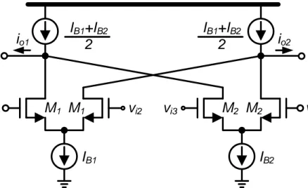
2.3 Continuous-Time Filters Employing Differential-Difference Amplifiers The differential-difference amplifier was first suggested in [10] as a versatile build-ing block offerbuild-ing a pair of differential inputs sharbuild-ing the same output (dual-input, single-output). The availability of multiple inputs makes this analog block attrac-tive for a number of applications such as filters [11], amplifiers [12], common-mode feedback circuits [13, 14], and input stages of fast comparators needed in a variety of analog-to-digital converters [15]. The simplified schematic of the single-stage fully-differential architecture is depicted in Figure 2.3. Two fully-differential pairs process the differential input signals with the drains of each differential pair being connected at the output leading to the differential output current given by
iout =io1 −io2 =Gm1(vi2−vi1) +Gm2(vi4−vi3) (2.2)
where Gmi is the small signal transconductance of the transistorsMi determined by
the bias current and transistor dimensions.
v
i2v
i1I
B1M
1M
1v
i3v
i4I
B2M
2M
2I
B1+I
B22
I
B1+I
B22
i
o1i
o2Figure 2.3: Single-stage differential difference amplifier.
significant noise contribution of the current sources used to compensate the DC current needed at the drain of the transistors; notice that the differential output referred current noise density due to these current sources is approximately equal to 8kT γGmp A2/Hz with the bias current source being equal to 0.5(IB1+IB2) and
Gmp being the transconductance of the bias current source transistors; ii) the power
efficiency of the OTA-C architecture is poor. The maximum AC voltage swing is limited by the linearity requirements which usually limit the signal magnitude to be less than the overdrive voltage of the transistors of the differential pairs; therefore, the voltage efficiency, defined here as the ratio of the peak value of the signal to the supply voltage, is usually small; e.g. less than 20 percent for medium linearity applications. With the aim of having first order results, consider the case of a single stage OTA employing a differential pair. First order estimation of the third order harmonic distortion HD3 leads to the following result for long channel devices [4]:
HD3 ∼= 1 32 vin VDSAT 2 (2.3)
wherevin is the amplitude of the input signal andVDSAT is the transistor’s overdrive
voltage. Thus for HD3 < −40 dB, the ratio of the input signal amplitude to the overdive voltage is limited to vin/VDSAT < 0.5. Assuming the quadratic model for
long-channel devices and (2.3), the OTA power efficiency P E can be obtained as
P E = vin VDD iO IB = vin VDD Gmvin IB = VDSAT VDD ×64×HD3. (2.4)
According to (2.4), the OTAP E is around 10 percent for the case ofHD3 =−40 dB (=0.01) and VDSAT/VDD = 0.3/1.8, but only 1 percent for the case of HD3 =−60 dB.
Source degeneration and other linearization techniques improve the voltage effi-ciency at the expense of a decrement in both current effieffi-ciency and voltage gain as well as an increase in noise level. Unfortunately, large source degeneration factors might not be feasible for advanced technologies where the power supplies are limited. On the other hand, current re-use techniques improve the OTA power efficiency since the same bias current is used for multiple purposes. In the next section, a current re-use biquad based on a DDA will be introduced.
2.4 Current Reused Gm Cells for Biquadratic Filters
One of the main issues of a biquad filter is that each implemented OTA is power hungry and noisy. Most of the research on biquad filters is focused on optimizing the design of the OTA by improving the linearity and attempting to reduce the power consumption; however, as predicted by (2.4), design tradeoffs limit its power efficiency.
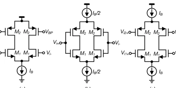
In Gm-C filter realizations such as the biquad shown in Figure 2.4, each of the OTAs is comprised of a voltage-to-current converter usually based on a conven-tional differential pair (CDP) as shown in Figure 2.5a. The N-type CDP realizes the voltage-to-current conversion while the P-type transistors are used as current sources to bias the arms of the CDP. Even if the CDP is an efficient voltage-to-current converter, the power dissipated by the P-type transistors is not used for signal processing thus reducing the circuit’s power efficiency; the noise introduced by the P-type transistors also reduces the OTA’s signal-to-noise ratio.
G
m1C
1G
m2C
2G
mRG
mFBV
i+V
i-V
o-V
o+V
x-V
x+Figure 2.4: Typical implementation of a Gm-C biquad filter.
In Figure 2.5b, the complimentary dual differential pair (DDP) based transcon-ductor which employs both N- and P-type differential pairs is shown. If the DDP is designed to have the same transconductance as the CDP of Figure 2.5a, and assum-ing that each differential pair provides equal transconductance, the current of the DDP can be halved. The output noise current is reduced from the CDP case since both of the noise contributors are halved. One downside is that the input capacitance increases.
VBP VBP V i-Vi+ IB IB/2 Vi+ V i-IB/2 IB Vi2+ V i1-IB Vi1+ V i2-(a) (b) (c) M1 M1 M2 M2 M2 M2 M1 M1 M1 M1 M2 M2
Figure 2.5: (a) Conventional differential pair, (b) dual differential pair using half the bias current, and (c) current-reuse differential difference amplifier.
however, the P-type transistors are arranged to produce a second transconductance which can be used in the biquad filter to make it more efficient. The DDA topol-ogy produces two transconductors for the same bias current as the CDP therefore reducing the average power per OTA by half.
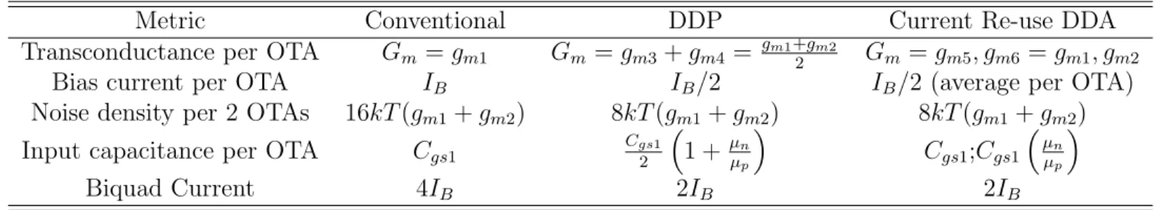
Table 2.2 compares the various performance metrics of the three topologies. For this table, it is assumed that the overdrive voltage is maintained constant for all transistors. The CDP employs two bias currents which contribute to 50 percent of the power and noise but not to signal power. The DDP topology is more efficient in terms of power due to the bias current being reused which results in a 50 per-cent reduction in power consumption for the same transconductance gain compared to the conventional differential pair case. Input capacitance for the DDP OTA ap-proximately doubles compared to the CDP since µn is approximately three times µp
for modern technologies and Cgs1 is around 50 percent of that of the conventional architecture due to the reduced bias current used. Even though the output noise
Table 2.2: Performance comparison between the conventional differential pair, dual differential pair, and proposed current reuse topology.
Metric Conventional DDP Current Re-use DDA
Transconductance per OTA Gm =gm1 Gm =gm3+gm4 = gm1+2gm2 Gm =gm5, gm6 =gm1, gm2
Bias current per OTA IB IB/2 IB/2 (average per OTA)
Noise density per 2 OTAs 16kT(gm1+gm2) 8kT(gm1+gm2) 8kT(gm1+gm2) Input capacitance per OTA Cgs1 Cgs21
1 + µnµp Cgs1;Cgs1 µn µp Biquad Current 4IB 2IB 2IB 16
density of the DDP is approximately half that of the DDA, total noise will be ap-proximately equal since two DDPs must be used for the same functionality as the DDA architecture. For the DDA architecture, the input capacitance for the biquad filter is similar to the CDP if the N-type differential pair is used. In the proposed biquadratic filter, the small capacitance N-type differential pair is used as the input stage to reduce loading in the preceding stage, while the P-type differential pairs with larger capacitances are used for internal filter nodes where the capacitance can easily be absorbed.
One drawback of biasing the two differential pairs with the same current is that design freedom becomes limited. If the bias current is set to provide the desired gm
for one of the differential pairs, only the transistor dimensions can be changed for the second differential pair which affects linear range. This drawback is somewhat alleviated by adding source degeneration resistors which give an extra design variable as shown in the following section.
2.5 DDA Based Biquad Filter Circuit Implementation
The transistor level schematic of the implemented current reused biquad is shown in Figure 2.6. A differential pair with source degeneration is used to implement the OTA. Since linearity is relaxed in this application, no additional linearization techniques are used because they would likely increase power consumption and hinder noise performance. The NMOS input OTA is biased with a PMOS differential pair with source degeneration which acts as the feedback OTA from Figure 2.4. The design uses a split tail-current design in order to not encounter the voltage drop across the source degeneration resistors which was found not to be feasible due to limited voltage headroom. Unfortunately the noise of the bias current source IB1 contributes the differential OTA output noise; this drawback, however, may not
be very significant as demonstrated in the following section. The full biquad filter of Figure 2.4 was implemented using two DDAs with the PMOS inputs receiving the output from the opposite DDA. The second N-type differential pair realizes the biquad lossy element that determines the filters Q-factor.
CMFB VCM RFB RFB R1 R1 C1 Vin+ V in-Vout- Vout+ CMFB VCM R2 R2 RQ RQ V x-Vx+ Vout- Vout+ VBP VBN M1 M1 MFB MFB M2 M2 MQ MQ MB1 MB1 MB1 MB1 MB2 MB2 MB2 MB2 V x-Vx+ C1 C2 C2
Figure 2.6: Transistor level implementation of proposed current-reused Gm-C biquad.
The transfer function of the implemented circuit is equal to the classical biquad circuit implementation of Figure 2.4
H(s) = Gm1Gm2 C1C2 s2+sGmR C1 + Gm2GmF B C1C2 (2.5)
where Gmi is the overall transconductance gain of the ith source-degenerated
differ-ential pair and are calculated as
Gm1 =
gm1 1 +gm1R1
Gm2 = gm2 1 +gm2R2 (2.7) GmR= gm,Q 1 +gmQRQ (2.8) GmF B = gm,F B 1 +gm,F BRF B (2.9) The common-mode detector needed for the common-mode feedback (CMFB) is non-invasive to the output avoiding extra resistive loading that can reduce the gain of the OTAs and limit their bandwidth due to extra parasitic capactiance. The realization of the CMFB amplifier is discussed in the following subsections.
Table 2.3 lists the sizes of the transistors used in the biquad filter. All three biquad filters used the same tranistor sizes in order to simplify the design. The source degeneration resistors were modified between stages to tune the transconductances to the needed value. Table 2.4 lists the sizes of the source degeneration resistors that were used.
Table 2.3: Biquad filter transistor sizes. Transistor Size (µm/µm)
M1, MQ 175/0.36
M2, MF B, MB2 126/0.18
MB1 84/0.36
2.5.1 Power Efficiency
The primary benefit of the proposed current-reused biquad is reduced current consumption which will double the power efficiency of the proposed topology if the voltage swing can be accommodated without increasing the power supply. In princi-ple, the voltage swing can be as large as the threshold voltage VT H of the transistors
Table 2.4: Biquad filter source degeneration resistor values. Component Biquad 1 Biquad 2 Biquad 3
R1 24 kΩ 800 Ω 2.3 kΩ
R2 1.6 kΩ 720 Ω 720 Ω
RF B 1.6 kΩ 4.4 kΩ 4.4 kΩ
RRQ 1.5 kΩ 1.4 kΩ 7 kΩ
if the OTA’s input and output signals are around 90 degrees out-of-phase, but signal swing could be limited toVT H/2 if they are around 180 degrees out-of-phase.
Fortu-nately, in the case of filters with low Q(less than 1), the signal swing at the filter’s internal nodes is less than or equal to the signal swing at the input which alleviates these issues. Also, in filters such as the one shown in Figure 2.4, the node Vx is
ap-proximately 90 degrees out-of-phase with respect the input and output signals which helps to avoid signal saturation.
2.5.2 Noise
It is well known that the reduction of input referred noise comes with the penalty of more power consumption and larger area since thermal noise is inversely propor-tional to capacitance. The DDA implementation in this design reduces the input referred noise without the need of additional power or increasing the area. In order to have a fair comparison in the noise performance of a biquad filter using DDAs and one using current-source loaded differential pairs, it is useful to look at the noise performance of just a single OTA in the system. Figure 2.7 shows the included noise sources for one of the OTAs in the DDA current-reused topology. Only the NMOS transistors with their noise sources are included because the PMOS transistors are all used to create a separate transconductor. The differential input referred noise of the transconductor is given by (2.10) where gmB1 is the transconductance of the
R1 M1 MB1 2 1 ,B n
i
i
n2,R1 R1 M1 MB1 2 1 ,B ni
2 1 ,R ni
2 1 , nv
v
n2,1 2 oni
i
on2 2 1 ,2
i
n R 2 2 ,B ni
2 2 ,B ni
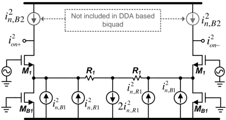
Not included in DDA based biquad
Figure 2.7: Noise sources for a single transconductor in the proposed DDA topology.
bias transistor MB1 and NR is the source degeneration factor gm1R1. To compare the noise to that of a current source loaded differential pair with source degeneration using the same split tail current topology, the input referred noise can be derived as in (2.11) where the only difference is the right-most term in the bracket which is the noise from the bias current source.
Vn,i,DDA2 = 8kT gm1 γ+NR+ γgmB1NR2 gm1 (2.10) Vn,i,conventional2 = 8kT gm1 γ+NR+ γgmB1NR2 gm1 + γgmB2(1 +NR) 2 gm1 ! (2.11) As shown in (2.10) and (2.11), the proposed topology will reduce the input re-ferred noise of the filter. As previously mentioned, it was necessary to split the tail current source in order to alleviate the voltage drop on the source degenera-tion resistor since the input common-mode voltage needs to be in the middle of the supply rails. For a current-source loaded OTA, it would be possible to raise the input common-mode voltage which would allow the tail current to be placed
be-tween the source-degeneration resistors. In this case, the noise from the tail current source would only be common-mode noise (ignoring differential mode noise due to mismatch) which would set the third term in the parenthesis in (2.11) to zero; the noise would thus be approximately equal to that of (2.10), the DDA case.
The filter was simulated in Cadence to test the noise performance. Figure 2.8 shows the input noise spectral density in the FIR filter’s passband range of 25 to 55 MHz. The noise spectral density is approximately 40 nV/Hz1/2 which is comparable to previously published results [6,7]. Integrated across the 30 MHz bandwidth of the maximum bandwidth of the matched filter, the total noise is 48 nV which is around 61 dB SNR for a 0 dBm input power. This result is better than the following sample-and-hold, therefore it will have negligble effect on the total SNR of the system.
25 30 35 40 45 50 55 38.5 39 39.5 40 40.5 41 41.5 42 42.5 43 Frequency (MHz) N o is e ( n V /H z 1 /2)
2.5.3 Common-Mode Feedback
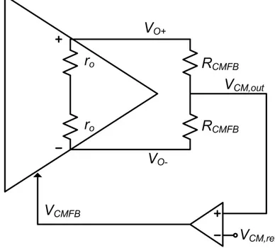
In order to reduce Q variations, high gain from the OTA is desired. Figure 2.9 shows an example of the classical way CMFB is employed [16]. The two resistors RCM F B at the output sense the output common-mode voltage VCM,out which is then
compared to a reference voltage VCM,ref which is the desired common-mode output.
This creates a control voltage VCM F B which is fed back to the amplifier to adjust
the output common-mode level. Because the two sense resistors are at the output node, they will be in parallel with the amplifier’s output resistance which causes a reduction in gain.
Figure 2.9: Classical CMFB topology which loads the amplifier output causing a reduction in gain.
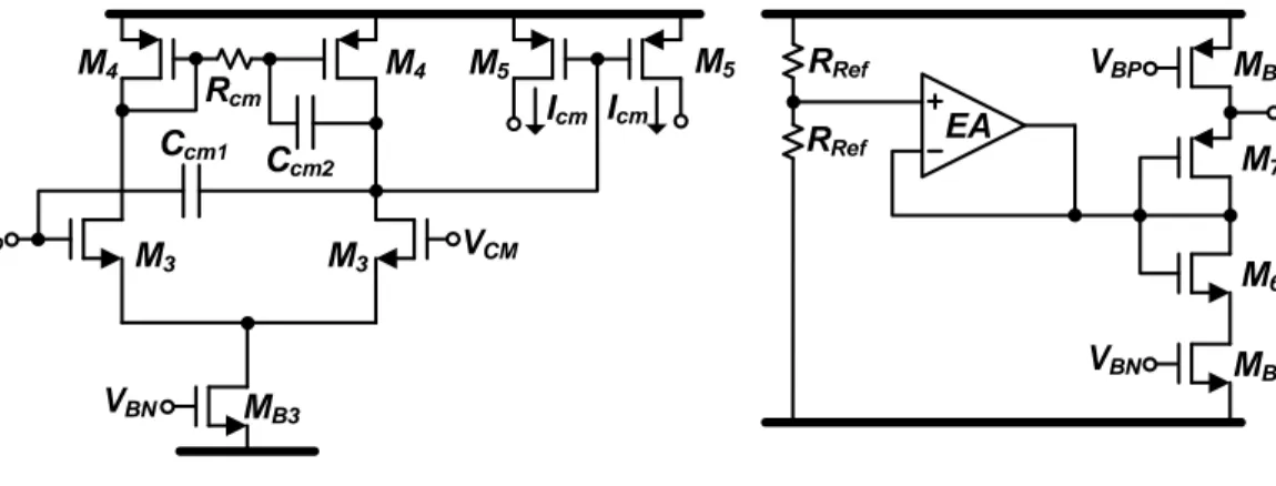
As shown in Figure 2.6, the implemented CMFB avoids loading of the output nodes by sensing the common-mode voltage from the node between the source
degen-eration resistors, albeit with a DC level shift. The implemented OTA to compensate for common-mode variations is shown in Figure 2.10a which is based on the topology presented in [17] with the capacitor Ccm1 added. The small signal model of one of the two common-mode loops is illustrated in Figure 2.11. Without the compensation network consisting ofRcm, Ccm1, andCcm2, there are three parasitic poles which are given by ωp1 =− 1 Ro1Cp2 (2.12) ωp2 =− 1 Ro2Cp3 (2.13) ωp3 =− 1 RsdCp1 (2.14) where Cpi is the parasitic capacitance at each respective node, Ro1 and Ro2 are the output resistances of the two amplification stages, andRsd is the source-degeneration
resistance from Figure 2.6 used to detect the common-mode signal.
MB3 M3 M3 Rcm Ccm1 C cm2 M4 M4 Vfb VCM VBN M5 M5 Icm Icm EA VBN VBP MB1 M6 M7 MB2 VCM RRef RRef (a) (b)
Figure 2.10: (a) Proposed common-mode feedback circuit with (b) replica circuit for proper generation of common-mode voltage reference VCM.
gm3 2 Ccm1 Ro1 Cp2 -gm5 Ro2 Cp3 RFB Cp1 Vi Vo
Figure 2.11: Small signal model of mode loop for one of the two common-mode loops.
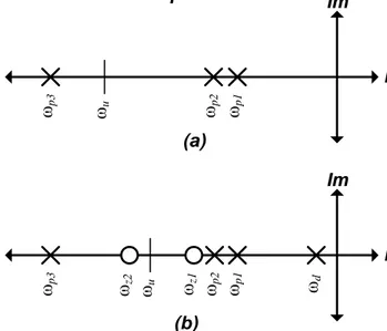
The location of these parasitic poles is illustrated in thes-plane diagram of Figure 2.12a. While ωp3 is located well beyond the unity gain frequency, ωp1 and ωp2 are located very near each other which will result in poor phase performance.
Im Re s-plane ωp1 ωp2 ωp3 ωu Im Re ωp1 ωp2 ωp3 ωz2 ωu ωz1 ωd (a) (b)
Figure 2.12: Pole-zero plot for the CMFB loop when the circuit is (a) uncompensated and (b) compensated.
Ccm1, andCcm2 were added. By adding the compensation network, the loop gain can be derived as in (2.15)-(2.19) HCM(s)≈H0 (1 +s/ωz1) (1 +s/ωz2) (1 +s/ωd) (1 +s/ωp1) (1 +s/ωp2) (1 +s/ωp3) (2.15) H0 =gm3gm5Ro1Ro2 (2.16) ωz1 =− 2 Rcm− gm14 Ccm2 (2.17) ωz2 =− gm3 2Ccm1 (2.18) ωd =− 1 gm4Ro1RcmCcm2 (2.19) where ωp1, ωp2, andωp3 are the same as the uncompensated case.
The s-plane representation of the compensated system is illustrated in Figure 2.12b. Because of the Miller effect, the dominant pole ωdis controlled with Rcm and
Ccm2. If Rcm is made large enough, i.e. greater than 1/gm4, the zero introduced through this network is pushed into the left-hand plane which helps to further sta-bilize the system. In this design, this zero was placed near ωp1 and ωp2. To further improve the stability, Ccm1 is added which will introduce another left-hand plane zero which can be placed near the unity gain frequency to provide a boost in phase margin. Notice thatCcm1 also introduces a negative capacitance atVf bwhich further
moves the parastic pole at that node to higher frequencies.
The purpose of Rcm and Ccm2 are twofold: i) make transistors M4 operate as a current mirror to properly bias M3 while reducing AC signal at medium and high frequencies and ii) Ccm2 makes the right hand side M4 transistor operate with its drain-gate connection shorted. This connection results in a low impedance node
of the M3 differential pair is shifted to high frequencies to assist with stability. Since the CMFB amplifier senses the common-mode voltage from the node be-tween the degeneration resistors, the measured DC voltage is not the desired DC voltage for the OTA output as in classical CMFB circuits; instead, it isVCM+VGS,p.
To force the output DC voltage to the required VDD/2, a replica circuit needs to be
implemented to generate the required reference voltage. The implemented circuit is shown in Figure 2.10b. A replica circuit of one branch of the proposed current reused biquad is used. Bias transistors Mb1 and Mb2 share the same bias circuit as the biquad to ensure that the same DC current is obtained in the replica circuit as the current-reuse OTA. Diode connecting M2 and forcing its drain to VDD/2 by
controlling its gate voltage with a local feedback loop is implemented with the error amplifier EA and Mb3 ensuring an accurate common-mode feedback reference volt-age generation. The implementation of the error amplifier is identical to that of the CMFB amplifier of Figure 2.10a except that the transistors M5 are not included.
Because the sensed common-mode voltage that is fed into the CMFB amplifier has a DC level shift from the true output common-mode voltage, a replica circuit is used to create the appropriate common-mode reference voltage. Figure 2.10b illustrates how the reference voltage for the CMFB amplifier is generated. The error amplifier EA used in the replica circuit is the OTA from Figure 2.10a without the additional transistors M5.
Transistor sizes for the CMFB network are listed in Table 2.5. The compensation resistor Rcm was 15 kΩ while the compensation capacitors Ccm1 and Ccm2 were 500 fF and 200 fF, respectively.
Table 2.5: Biquad filter CMFB transistor sizes. Component Size (µm/µm) M3,MB3 42/0.36 M4 112/0.36 M5, M7, MB2 126/0.18 M6,MB1 84/0.36 M8 56/0.18 2.6 Measurement Results
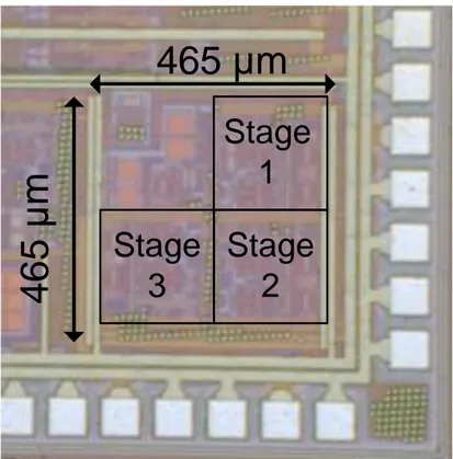
The Gm-C filter was designed and fabricated in 0.18 µm SOI CMOS process by Jazz Semiconductor [18]. Figure 2.13 shows the microphotograph of the fabricated anti-alias filter. The total chip area is 0.21 mm2.
To measure the frequency response of the filter, the filter was connected to a network analyzer. Figure 2.14 shows the magnitude response of the fabricated filter. The -3 dB corner frequency is approximately 65 MHz. The in-band group delay of the anti-alias filter is shown in Figure 2.15. From 25 MHz to 55 MHz, the maximum passband range of the FIR filter, there is about 3.5 ns total variation in the group delay.
To test the linearity of the filter, two input tones were applied at 39.5 MHz and 40.5 MHz. The power of the two input tones were swept while measuring the total power of the two fundamental tones and two IM3 tones at the output as shown in Fig-ure 2.16. The measFig-ured input referred third-order intercept (IIP3) is approximately 12.0 dBm with a 1-dB compression point of 0 dBm. With source degeneration as the only method of linearity improvement and the inclusion of additional current source transistors which limit available voltage headroom, these results are expected.
465 µm
4
6
5
µ
m
Stage
3
Stage
1
Stage
2
Figure 2.13: Microphotograph of the fabricated low-power Gm-C filter.
Table 2.6 with the Figure of Merrit (FoM) used defined as
FoM = IIP3×f-3dB,MHz×N PmW
(2.20)
where f-3dB,MHz is the -3 dB frequency in MHz, N is the filter order, and PmW is the filter’s power consumption in mW. It is seen that this work compares favorably to the state-of-the-art as its FoM greatly exceeds that of the previously published results predominantly because the power per pole in this design is vastly superior.
106 107 108 -70 -60 -50 -40 -30 -20 -10 0 Frequency (Hz) G a in ( d B )
Figure 2.14: Magnitude response of the Gm-C filter.
20 25 30 35 40 45 50 55 60 26.5 27 27.5 28 28.5 29 29.5 30 30.5 31 31.5 Frequency (MHz) G ro u p D e la y ( n s )
-20 -15 -10 -5 0 5 10 15 -80 -70 -60 -50 -40 -30 -20 -10 0 10 20 Input Power (dBm) O u tp u t P o w e r (d B m ) OIP3 = 12.0 dBm
Figure 2.16: Linearity measurement for the Gm-C filter.
Table 2.6: Comparison to previously published results. Specification [5] [6] [7] [9] This Work
Technology (nm) 180 130 350 180 180
Bandwidth (MHz) 50-200 200 200 50-300 65
Filter Order 3 2 7 3 6
Input Noise (nV/√Hz) 5 22 65 3 40
IIP3 (dBm) 16 14 11 19 12
Power per Pole (mW) 7.8 10.4 8.6 68.3 1.34
2.7 Conclusion
A Gm-C anti-alias filter has been designed for low power applications. Since signal-to-noise-and-distortion ratio (SNDR) for the final application is not critical, the focus of the design was put into power efficiency instead of linearity. The power efficiency was optimized by 50 percent compared to conventional implementations. The architecture was implemented with a current-reuse technique which allows bias-ing two OTAs with the same DC current. With the implementation of the current-reuse technique, the need of extra bias current sources is avoided. Additionally, the noise performance is improved since fewer transistors will be contributing to the fil-ter’s noise. Source degeneration resistors were used to improve the circuit’s linearity. The CMFB circuitry measures the common-mode signal from the source degenera-tion resistors and thus does not load the output of the OTA helping maintain OTA gain. The filter was implemented in Jazz 0.18 µm SOI CMOS and achieves the best power consumption per filter pole compared to previously reported results.
3. A 128-TAP HIGHLY TUNABLE CMOS IF MATCHED FILTER FOR PULSED RADAR APPLICATIONS
In the radar system of Figure 1.2, there is a matched filter which is used to eliminate as much as possible the surrounding thermal noise and blockers that are present in the received signal spectrum. In designing the matched filter, it would be beneficial to reduce the bandwidth as much as possible in order to improve the SNR; however, filter bandwidths that are too narrow would not be able to pass the received pulse without distortion of the pulse envelope in the time-domain. This effect is shown in Figure 3.1. The top waveform in the figure is a 40 MHz input pulsed for 100 ns. When the filter bandwidth is too small, there will be excessive spreading in the time domain. This effect is illustrated in the second waveform which is the case when the filter bandwidth is 3 MHz. Ideally, the filter bandwidth should be approximately the inverse of the pulse width, or 10 MHz in this case. The third waveform shows the case for the 10 MHz bandwidth. The pulse passes without too much spreading in the time domain. The bottom waveform is the case when the bandwidth is wider than necessary, or 30 MHz in this case. There is little difference in the envelope of the 10 MHz and 30 MHz waveforms which means that the filter bandwidth could be reduced in the final case to achieve a better SNR. Therefore the matched filter should be designed with a bandwidth large enough to pass the received pulse without causing extreme time-domain distortion while being narrow enough to maximize receiver SNR.
0 0.1 0.2 0.3 0.4 0.5 0.6 0.7 0.8 0.9 1 -1 -0.5 0 0.5 1
Input - 100 ns pulse length
0 0.1 0.2 0.3 0.4 0.5 0.6 0.7 0.8 0.9 1 -1 -0.5 0 0.5 1 3 MHz Bandwidth Filtering 0 0.1 0.2 0.3 0.4 0.5 0.6 0.7 0.8 0.9 1 -1 -0.5 0 0.5 1 10 MHz Bandwidth Filtering 0 0.1 0.2 0.3 0.4 0.5 0.6 0.7 0.8 0.9 1 -1 -0.5 0 0.5 1 Time (us) 30 MHz Bandwidth Filtering
Figure 3.1: Matched filter example with 100 ns pulse time. Top waveform is the input. The second waveform is a filter with 3 MHz bandwidth which is too small for the pulse. The second waveform is the matched filter bandwidth of 10 MHz. The bottom waveform is a 30 MHz bandwidth filter which is excessive.
In current applications, the matched filter has typically been implemented with SAW and BAW filters. The disadvantage of these filters is that they are bulky, untunable, temperature senstive, and must be off chip which is expensive compared to on-chip solutions. In this dissertation, an FIR filter structure is introduced which is widely tunable in bandwidth in order for it to be optimized depending on the pulse width of the transmitted signal.
Most previously reported FIR filters typically fall into one of two categories. References [19–28] all use switched capacitor designs which typically need one am-plifier per tap whereas the new trend in research tends toward switched-current techniques [29–46]. Of these, only [39, 40] have reported tunable designs; however, these are lowpass filters which can be adjusted in bandwidth by varying the clock rate. If the transfer functions were modified to a bandpass shape, adjusting the clock rate would not only vary the bandwidth but could also have the unfortunate side effect of varying the filter’s center frequency.
In this chapter, an FIR bandpass matched filter design is presented which has a tunable bandwidth from 3 to 30 MHz while being centered at 40 MHz. This fil-ter could potentially replace the SAW or BAW filfil-ters that are typically used while moving the filtering function on chip where it can be nearer to the receiver and DSP reducing overall cost. The proposed FIR filter employs 128-taps realized by transconductors, switches, capacitors, and 34 non-overlapping clock phases. The transconductors are highly tunable which allows them to realize various filter band-widths without modifying the filter’s clock rate of 150 MHz. The filter was designed in a Jazz 0.18µm CMOS SOI process [18] and consumed 450 mW with an attenuation greater than 40 dB at 10 MHz beyond the -3 dB frequency.
3.1 FIR Filter System Level Design
To meet the requirements of the radar receiver, the filter needs to be tunable in bandwidth from 3 to 30 MHz with greater than 40 dB attenuation just 10 MHz beyond the passband while maintaining a linear phase response, i.e. constant group delay. Because this is difficult to achieve with conventional analog filters, a discrete-time FIR topology was chosen. Due to their simplicity, FIR filters can usually be implemented at a much higher order than would be conceivable with Gm-C, active-RC, or switched-capacitor techniques. FIR filters are process, voltage, and tempera-ture (PVT) variation tolerant and usually can be scaled up or down in frequency by scaling the clock frequency. The discrete time FIR filter can have a constant group delay whose value only depends on the clock rate and number of taps.
FIR filters can be described by the equation
H(z) =
N X
n=0
αnz−n (3.1)
where N is the number of taps. If the coefficients of 3.1 are symmetric, meaning
αn =αN−n,0≤n≤N, (3.2)
then the filter will have linear phase response which provides constant group delay across the frequency band [47]. For the pulsed-Doppler radar filter, constant group delay is desirable because it will allow the received signal to pass the desired inter-mediate frequency (IF) pulse without causing time-domain distortion in the pulse shape.
Matlab was used to obtain the required order and coefficients needed for each
The bandwidth was tunable from approximately 3 MHz to 30 MHz. In order to obtain the required attenuation of -40 dB at 10 MHz beyond the passband, four identical FIR filters were cascaded as illustrated in Figure 3.2. Since the operation of the FIR filter in this application is discrete-time in nature, the input was first sampled with a sample-and-hold circuit. As will be seen during the discussion of the filter architecture, the input to the filter must remain constant during each clock cycle; therefore, a time-interleaved sample-and-hold topology was used to provide a constant input throughout the entire clock cycle. Using Matlab, the required FIR
filter coefficients αn were calculated as listed in Table 3.1.
32 – Tap FIR M U X Time Interleaved SH 32 – Tap FIR M U X 32 – Tap FIR M U X 32 – Tap FIR M U X Vout Vin BW Select
Figure 3.2: Proposed 128-tap programmable FIR bandpass filter block diagram in-cluding time-interleaved sample-and-hold followed by four 32-tap FIR filters with controllable bandwidth.
Table 3.1: FIR filter coefficients to meet the desired filter bandwidths. Coefficient 3 MHz 4 MHz 6 MHz 8 MHz 10 MHz 12 MHz 15 MHz 20 MHz 25 MHz 30 MHz α0,32 0 0 0 0 0 0 0 0 0 0 α1,31 0.0081 0.0005 -0.0028 -0.0018 0.0002 0.0020 0.0026 -0.0010 -0.0026 0.0015 α2,30 -0.0012 -0.0002 0.0004 0.0004 0.0002 -0.0001 -0.0004 -0.0001 0.0004 0.0001 α3,29 -0.0157 -0.0040 0.0051 0.0061 0.0043 0.0008 -0.0043 -0.0049 0.0022 0.0056 α4,28 0.0067 0.0024 -0.0017 -0.0028 -0.0027 -0.0016 0.0007 0.0028 0.0010 -0.0025 α5,27 0.0263 0.0123 -0.0039 -0.0101 -0.0122 -0.0107 -0.0035 0.0095 0.0109 -0.0025 α6,26 -0.0186 -0.0107 0 0.0053 0.0084 0.0094 0.0070 -0.0023 -0.0089 -0.0058 α7,25 -0.0380 -0.0260 -0.0069 0.0046 0.0133 0.0192 0.0209 0.0083 -0.0103 -0.0213 α8,24 0.0387 0.0305 0.0150 0.0039 -0.0059 -0.0147 -0.0228 -0.0212 -0.0061 0.0161 α9,23 0.0464 0.0412 0.0283 0.0173 0.0061 -0.0057 -0.0208 -0.0331 -0.0283 -0.0052 α10,22 -0.0658 -0.0644 -0.0549 -0.0443 -0.0317 -0.0165 0.0069 0.0388 0.0544 0.0475 α11,21 -0.0465 -0.0493 -0.0490 -0.0457 -0.0405 -0.0330 -0.0191 0.0059 0.0276 0.0443 α12,20 0.0948 0.1070 0.1188 0.1214 0.1198 0.1140 0.0982 0.0601 0.0150 -0.0422 α13,19 0.0349 0.0414 0.0496 0.0538 0.0566 0.0584 0.0586 0.0542 0.0453 0.0290 α14,18 -0.1176 -0.1439 -0.1820 -0.2049 -0.2241 -0.2417 -0.2628 -0.2857 -0.2963 -0.2920 α15,17 -0.0130 -0.0163 -0.0212 -0.0244 -0.0272 -0.0301 -0.0341 -0.0399 -0.0451 -0.0505 α16 0.1262 0.1586 0.2089 0.2417 0.2719 0.3027 0.3467 0.4152 0.4806 0.5578 38
In order to implement the desired FIR transfer function, first consider the circuit illustrated in Figure 3.3a which includes 32 transconductors, one capacitor, and switches controlled by the set of 34 non-overlapping clock phases shown in Figure 3.3b. The input voltage which is constant during an entire clock cycle is converted into a set of currents which, depending on the current clock phase, charge/discharge the capacitor. The total charge accumulated on the capacitor after 32 clock cycles and measured at the end of the process during clock phase φ34 is
QC1[φ34] = 32
X
i=1
gmivin[φi]Tck (3.3)
where Tck is the period of the master clock clk. Since the charge is accumlated on a
capacitor, the voltage at the evaluation phase is
VO[φ34] = Tck C 32 X i=1 gmivin[φi]. (3.4)
Employing the z-transform of the discrete time equation leads to
VO[z] φ34 = Tck C 32 X i=1 gmiz−i ! Vin[z] = Tck C gm1Vin[z] 32 X i=1 αiz−i ! (3.5)
where the coefficient α1 = 1 and all other coefficientsα2−32=gm2−32/gm1. It is clear that (3.5) resembles a typical discrete time filter transfer function thus enabling an FIR topology where the filter coefficients are implemented by ratios of transconduc-tances making the overall filter shape less sensitive to PVT variations; the in-band gain, however is sensitive to PVT variations since gm1 itself will be susceptibe to PVT variations causing errors in the magnitude of the passband gain.
Vin f1 Vo (a) Gm1 f33 Gm2 Gm32 f1 f2 f3 (b) f33 f34 clk C f2 f32 f34
Figure 3.3: Single-tap implementation illustrating a) system level which includes 32 tunable transconductor cells, charge accumulation capacitor, and switches with b) 34 non-overlapping clock phases.
Although this architecture is interesting, filter latency is excessive; the overall sampling rate is only Tck/34 which is too slow for the intended application. The
circuit of Figure 3.3a can be expanded to the proposed FIR filter topology illustrated in Figure 3.4. This filter adds additional capacitors and a multiplexer (MUX) to allow the output signal to be taken from one capacitor each clock cycle. (3.5) can thus be extended to obtain the overall transfer function of
VO[z] Vin[z] = gm1Tck C 32 X i=1 αiz−i ! . (3.6)