1
1964fb
TYPICAL APPLICATION
DESCRIPTION
200mA, Low Noise,
Low Dropout Negative
Micropower Regulator
The LT®1964 is a micropower low noise, low dropout nega-tive regulator. The device is capable of supplying 200mA of output current with a dropout voltage of 340mV. Low quiescent current (30μA operating and 3μA shutdown) makes the LT1964 an excellent choice for battery-pow-ered applications. Quiescent current is well controlled in dropout.
Other features of the LT1964 include low output noise. With the addition of an external 0.01μF bypass capacitor, output noise is reduced to 30μVRMS over a 10Hz to 100kHz bandwidth. The LT1964 is capable of operating with small capacitors and is stable with output capacitors as low as 1μF. Small ceramic capacitors can be used without the necessary addition of ESR as is common with other regulators. Internal protection circuitry includes reverse output protection, current limiting, and thermal limiting. The device is available with a fi xed output voltage of –5V and as an adjustable device with a –1.22V reference volt-age. The LT1964 regulators are available in a low profi le (1mm) ThinSOT and the low profi le (0.75mm) 8-pin
(3mm × 3mm) DFN packages.
L, LT, LTC and LTM are registered trademarks of Linear Technology Corporation. ThinSOT is a trademark of Linear Technology Corporation. All other trademarks are the property of their respective owners.
FEATURES
APPLICATIONS
n Low Noise: 30μVRMS (10Hz to 100kHz) n Low Quiescent Current: 30μA
n Low Dropout Voltage: 340mV n Output Current: 200mA n Fixed Output Voltage: –5V
n Adjustable Output from –1.22V to – 20V n Positive or Negative Shutdown Logic
n 3μA Quiescent Current in Shutdown
n Stable with 1μF Output Capacitor
n Stable with Aluminum, Tantalum, or Ceramic
Capacitors
n Thermal Limiting
n Low Profi le (1mm) ThinSOT™ and (0.75mm) 8-Pin
3mm × 3mm DFN Packages
n Battery-Powered Instruments
n Low Noise Regulator for Noise-Sensitive
Instrumentation
n Negative Complement to LT1761 Family of
Positive LDOs
–5V Low Noise Regulator
10Hz to 100kHz Output Noise 1964 TA01a GND SHDN BYP IN OUT LT1964-5 1μF 10μF 0.01μF VIN –5.4V TO –20V –5V AT 200mA 30μVRMS NOISE VOUT 100μV/DIV 1ms/DIV 1964 TA01b 30μVRMS
2
1964fb
ABSOLUTE MAXIMUM RATINGS
IN Pin Voltage ... ±20V OUT Pin Voltage (Note 11) ...±20V OUT to IN Differential Voltage (Note 11) ... –0.5V, 20V ADJ Pin Voltage
(with Respect to IN Pin) (Note 11) ... –0.5V, 20V BYP Pin Voltage
(with Respect to IN Pin) ... ±20V
SHDN Pin Voltage
(with Respect to IN Pin) (Note 11) ... –0.5V, 35V
(Note 1) LT1964 LT1964-SD TOP VIEW DD PACKAGE 8-LEAD (3mm s 3mm) PLASTIC DFN 5 6 7 8 9 4 3 2 1 OUT OUT ADJ SHDN IN IN GND BYP TJMAX = 125°C, θJA = 40°C/W, θJC = 16°C/W (NOTE 13)
EXPOSED PAD (PIN 9) IS IN, MUST BE SOLDERED TO PCB
5 OUT
4 ADJ GND 1
TOP VIEW
S5 PACKAGE 5-LEAD PLASTIC SOT-23 IN 2
SHDN 3
TJMAX = 150°C, θJA ≈125°C/W to 250°C/W
(NOTE 13)
SEE THE APPLICATIONS INFORMATION SECTION
LT1964-BYP LT1964-5 5 OUT 4 ADJ GND 1 TOP VIEW S5 PACKAGE 5-LEAD PLASTIC SOT-23 IN 2
BYP 3
TJMAX = 150°C, θJA ≈125°C/W to 250°C/W
(NOTE 13)
SEE THE APPLICATIONS INFORMATION SECTION
5 OUT
4SHDN GND 1
TOP VIEW
S5 PACKAGE 5-LEAD PLASTIC SOT-23 IN 2
BYP 3
TJMAX = 150°C, θJA ≈125°C/W to 250°C/W
(NOTE 13)
SEE THE APPLICATIONS INFORMATION SECTION
PIN CONFIGURATION
ORDER INFORMATION
LEAD FREE FINISH TAPE AND REEL PART MARKING* PACKAGE DESCRIPTION TEMPERATURE RANGE
LT1964ES5-SD#PBF LT1964ES5-SD#TRPBF LTVX 5-Lead Plastic SOT-23 –40°C to 125°C LT1964ES5-BYP#PBF LT1964ES5-BYP#TRPBF LTVY 5-Lead Plastic SOT-23 –40°C to 125°C
LT1964ES5-5#PBF LT1964ES5-5#TRPBF LTVZ 5-Lead Plastic SOT-23 –40°C to 125°C
LT1964EDD#PBF LT1964EDD#TRPBF LDVM 8-Lead (3mm × 3mm) Plastic DFN –40°C to 125°C LT1964IS5-SD#PBF LT1964IS5-SD#TRPBF LTVX 5-Lead Plastic SOT-23 –40°C to 125°C LT1964IS5-BYP#PBF LT1964IS5-BYP#TRPBF LTVY 5-Lead Plastic SOT-23 –40°C to 125°C
LT1964IS5-5#PBF LT1964IS5-5#TRPBF LTVZ 5-Lead Plastic SOT-23 –40°C to 125°C
LT1964IDD#PBF LT1964IDD#TRPBF LDVM 8-Lead (3mm × 3mm) Plastic DFN –40°C to 125°C
SHDN Pin Voltage
(with Respect to GND Pin) ...–20V, 15V Output Short-Circuit Duration ... Indefi nite Operating Junction Temperature (E, I Grade)
Range (Note 10) ... – 40°C to 125°C Storage Temperature Range ... –65°C to 150°C Lead Temperature (Soldering, 10 sec)
3
1964fb
ELECTRICAL CHARACTERISTICS
The l denotes the specifi cations which apply over the full operating temperature range, otherwise specifi cations are at TA = 25°C.
PARAMETER CONDITIONS MIN TYP MAX UNITS
Regulated Output Voltage (Notes 3, 9)
LT1964-5 VIN = –5.5V, ILOAD = –1mA
–20V < VIN < –6V, –200mA < ILOAD < –1mA l
–4.925 –4.850 –5 –5 –5.075 –5.150 V V ADJ Pin Voltage
(Notes 2, 3, 9)
LT1964 VIN = –2V, ILOAD = –1mA
–20V < VIN < –2.8V, –200mA < ILOAD < –1mA l
–1.202 –1.184 –1.22 –1.22 –1.238 –1.256 V V Line Regulation LT1964-5 ΔVIN = –5.5V to –20V, ILOAD = –1mA
LT1964 (Note 2) ΔVIN = –2.8V to –20V, ILOAD = –1mA
l l 151 50 12 mV mV Load Regulation LT1964-5 VIN = –6V, ΔILOAD = –1mA to –200mA
VIN = –6V, ΔILOAD = –1mA to –200mA l
15 35
50
mV mV LT1964 VIN = –2.8V, ΔILOAD = –1mA to –200mA
VIN = –2.8V, ΔILOAD = –1mA to –200mA l
2 7 15 mV mV Dropout Voltage VIN = VOUT(NOMINAL) (Notes 4, 5) ILOAD = –1mA ILOAD = –1mA l 0.1 0.15 0.19 V V ILOAD = –10mA ILOAD = –10mA l 0.15 0.20 0.25 V V ILOAD = –100mA ILOAD = –100mA l 0.26 0.33 0.39 V V ILOAD = –200mA ILOAD = –200mA l 0.34 0.42 0.49 V V GND Pin Current VIN = VOUT(NOMINAL) (Notes 4, 6) ILOAD = 0mA ILOAD = –1mA ILOAD = –10mA ILOAD = –100mA ILOAD = –200mA l l l l l 30 85 300 1.3 2.5 70 180 600 3 6 μA μA μA mA mA
ORDER INFORMATION
LEAD BASED FINISH TAPE AND REEL PART MARKING* PACKAGE DESCRIPTION TEMPERATURE RANGE
LT1964ES5-SD LT1964ES5-SD#TR LTVX 5-Lead Plastic SOT-23 –40°C to 125°C
LT1964ES5-BYP LT1964ES5-BYP#TR LTVY 5-Lead Plastic SOT-23 –40°C to 125°C
LT1964ES5-5 LT1964ES5-5#TR LTVZ 5-Lead Plastic SOT-23 –40°C to 125°C
LT1964EDD LT1964EDD#TR LDVM 8-Lead (3mm × 3mm) Plastic DFN –40°C to 125°C
LT1964IS5-SD LT1964IS5-SD#TR LTVX 5-Lead Plastic SOT-23 –40°C to 125°C
LT1964IS5-BYP LT1964IS5-BYP#TR LTVY 5-Lead Plastic SOT-23 –40°C to 125°C
LT1964IS5-5 LT1964IS5-5#TR LTVZ 5-Lead Plastic SOT-23 –40°C to 125°C
LT1964IDD LT1964IDD#TR LDVM 8-Lead (3mm × 3mm) Plastic DFN –40°C to 125°C
Consult LTC Marketing for parts specifi ed with wider operating temperature ranges. *The temperature grade is identifi ed by a label on the shipping container. For more information on lead free part marking, go to: http://www.linear.com/leadfree/
4
1964fb
Note 1: Stresses beyond those listed under Absolute Maximum Ratings may cause permanent damage to the device. Exposure to any Absolute Maximum Rating condition for extended periods may affect device reliability and lifetime
Note 2: The LT1964 (adjustable version) is tested and specifi ed for these conditions with the ADJ pin connected to the OUT pin.
Note 3: Operating conditions are limited by maximum junction temperature. The regulated output voltage specifi cation will not apply for all possible combinations of input voltage and output current. When operating at maximum input voltage, the output current range must be limited. When operating at maximum output current, the input voltage range must be limited.
Note 4: To satisfy requirements for minimum input voltage, the LT1964 (adjustable version) is tested and specifi ed for these conditions with an external resistor divider (two 249k resistors) for an output voltage of –2.44V. The external resistor divider will add a 5μA DC load on the output.
Note 5: Dropout voltage is the minimum input to output voltage differential needed to maintain regulation at a specifi ed output current. In dropout, the output voltage will be equal to: (VIN + VDROPOUT).
Note 6: GND pin current is tested with VIN = VOUT(NOMINAL) and a current
source load. This means the device is tested while operating in its dropout region. This is the worst-case GND pin current. The GND pin current will decrease slightly at higher input voltages.
Note 7: ADJ pin bias current fl ows out of the ADJ pin.
Note 8: Positive SHDN pin current fl ows into the SHDN pin. SHDN pin current is included in the GND pin current specifi cation.
Note 9: For input-to-output differential voltages greater than 7V, a 50μA load is needed to maintain regulation.
Note 10: The LT1964 is tested and specifi ed under pulse load conditions such that TJ≅ TA. The LT1964E is tested at TA = 25°C. Performance at
–40°C to 125°C is assured by design, characterization and correlation with statistical process controls. The LT1964I is guaranteed over the full –40°C to 125°C operating junction temperature range.
Note 11: A parasitic diode exists internally on the LT1964 between the OUT, ADJ and SHDN pins and the IN pin. The OUT, ADJ and SHDN pins cannot be pulled more than 0.5V more negative than the IN pin during fault conditions, and must remain at a voltage more positive than the IN pin during operation.
Note 12: For the LT1964-BYP, this specifi cation accounts for the operating threshold of the SHDN pin, which is tied to the IN pin internally. For the LT1964-SD, the SHDN threshold must be met to ensure device operation.
Note 13: Actual thermal resistance (θJA) junction to ambient will be a
function of board layout. See the Thermal Considerations section in the Applications Information.
ELECTRICAL CHARACTERISTICS
The l denotes the specifi cations which apply over the full operating temperature range, otherwise specifi cations are at TA = 25°C.Output Voltage Noise COUT = 10μF, CBYP = 0.01μF, ILOAD = –200mA, BW = 10Hz to 100kHz 30 μVRMS
ADJ Pin Bias Current (Notes 2, 7) 30 100 nA
Minimum Input Voltage (Note 12) ILOAD = –200mA LT1964-BYP LT1964-SD l l –1.9–1.6 –2.8 –2.2 V V Shutdown Threshold VOUT = Off to On (Positive)
VOUT = Off to On (Negative)
VOUT = On to Off (Positive)
VOUT = On to Off (Negative)
l l l l –0.250.25 1.6 –1.9 0.8 –0.8 2.1 –2.8 V V V V
SHDN Pin Current (Note 8) VSHDN = 0V VSHDN = 15V VSHDN = –15V –1 ±0.1 6 –3 1 15 –9 μA μA μA
Quiescent Current in Shutdown VIN = –6V, VSHDN = 0V l 3 10 μA
Ripple Rejection VIN – VOUT = –1.5V(Avg), VRIPPLE = 0.5VP-P,
fRIPPLE = 120Hz, ILOAD = –200mA
46 54 dB
Current Limit VIN = –6V, VOUT = 0V
VIN = VOUT(NOMINAL) –1.5V, ΔVOUT = 0.1V l 220
350 mA
mA Input Reverse Leakage Current VIN = 20V, VOUT, VADJ, VSHDN = Open Circuit l 1 mA
5
1964fb
TYPICAL PERFORMANCE CHARACTERISTICS
Quiescent Current
LT1964-5
Output Voltage LT1964 ADJ Pin Voltage
LT1964-5
Quiescent Current LT1964 Quiescent Current
LT1964-5 GND Pin Current Typical Dropout Voltage Guaranteed Dropout Voltage Dropout Voltage
OUTPUT CURRENT (mA) 0 500 450 400 350 300 250 200 150 100 50 0 1964 G01 –40 –80 –120 –160 –200 DROPOUT VOLTAGE (mV) TJ = 125°C TJ = 25°C
OUTPUT CURRENT (mA) 0 500 450 400 350 300 250 200 150 100 50 0 1964 G02 –40 –80 –120 –160 –200 DROPOUT VOLTAGE (mV) TJ ≤ 125°C = TEST POINT TJ ≤ 25°C TEMPERATURE (°C) 500 450 400 350 300 250 200 150 100 50 0 1964 G03 DROPOUT VOLTAGE (mV) IL = –100mA IL = –50mA IL = –10mA IL = –1mA IL = –200mA –50 –25 0 25 50 75 100 125 TEMPERATURE (°C) –50 –45 –40 –35 –30 –25 –20 –15 –10 –5 0 1964 G04
QUIESCENT CURRENT (μA)
VIN = –6V RL = 250k (∞ FOR LT1964-5) IL = –5μA (0 FOR LT1964-5) –50 –25 0 25 50 75 100 125 VSHDN = VIN VSHDN = 0V TEMPERATURE (°C) –5.12 –5.09 –5.06 –5.03 –5.00 –4.97 –4.94 –4.91 –4.88 1964 G05 OUTPUT VOLTAGE (V) IL = –1mA –50 –25 0 25 50 75 100 125 TEMPERATURE (°C) –1.240 –1.235 –1.230 –1.225 –1.220 –1.215 –1.210 –1.205 –1.200 1964 G06
ADJ PIN VOLTAGE (V)
IL = –1mA –50 –25 0 25 50 75 100 125 INPUT VOLTAGE (V) –40 –35 –30 –25 –20 –15 –10 –5 –0 1964 G07
QUIESCENT CURRENT (μA)
0 –1 –2 –3 –4 –5 –6 –7 –8 –9 –10 TJ = 25°C RL = ∞ VSHDN = VIN VSHDN = 0V INPUT VOLTAGE (V) –40 –35 –30 –25 –20 –15 –10 –5 –0 1964 G08
QUIESCENT CURRENT (μA)
0 –1 –2 –3 –4 –5 –6 –7 –8 –9 –10 TJ = 25°C RL = 250k IL = –5μA VSHDN = VIN VSHDN = 0V INPUT VOLTAGE (V) –3.0 –2.5 –2.0 –1.5 –1.0 –0.5 0 1964 G09
GND PIN CURRENT (mA)
0 –1 –2 –3 –4 –5 –6 –7 –8 –9 –10 TJ = 25°C VSHDN = VIN *FOR VOUT = –5V RL = 25 IL = –200mA* RL = 50 IL = –100mA* RL = 100 IL = –50mA* RL = 500 IL = –10mA*
6
1964fb
TYPICAL PERFORMANCE CHARACTERISTICS
SHDN Pin Input Current SHDN Pin Input Current ADJ Pin Bias Current LT1964 GND Pin Current GND Pin Current vs ILOAD SHDN Pin Thresholds
–3.0 –2.5 –2.0 –1.5 –1.0 –0.5 0 1964 G10
GND PIN CURRENT (mA)
0 –1 –2 –3 –4 –5 –6 –7 –8 –9 –10 RL = 12.2Ω IL = –100mA* RL = 24.4Ω IL = –50mA* RL = 122Ω IL = –10mA* TJ = 25°C; VSHDN = VIN; *FOR VOUT = –1.22V RL = 6.1Ω IL = –200mA* INPUT VOLTAGE (V) –4.0 –3.5 –3.0 –2.5 –2.0 –1.5 –1.0 –0.5 0 1964 G11
GND PIN CURRENT (mA)
0 –40 –80 –120 –160 –200
VIN = VOUT(NOMINAL) – 1V
TJ = –50°C
TJ = 25°C
TJ = 125°C
OUTPUT CURRENT (mA)
2.5 2.0 1.5 1.0 0.5 0 –0.5 –1.0 –1.5 –2.0 –2.5 1964 G12 SHDN PIN VOLTAGE (V) ON ON OFF TEMPERATURE (°C) –50 –25 0 25 50 75 100 125 10 8 6 4 2 0 –2 –4 –6 –8 –10 1964 G13 SHDN
PIN INPUT CURRENT (μA)
SHDN PIN VOLTAGE (V)
–10 –8 –6 –4 –2 0 2 4 6 8 10
TJ = 25°C POSITIVE CURRENT FLOWS INTO THE PIN
12 9 6 3 0 –3 –6 –9 1964 G14 SHDN
PIN INPUT CURRENT (μA)
TEMPERATURE (°C) –50 –25 0 25 50 75 100 125 VSHDN = 15V VSHDN = –15V VIN = –15V POSITIVE CURRENT FLOWS INTO THE PIN
–70 –60 –50 –40 –30 –20 –10 0 1964 G15
ADJ PIN BIAS CURRENT (nA)
TEMPERATURE (°C)
7
1964fb
Input Ripple Rejection
LT1964-BYP
Minimum Input Voltage
LT1964, LT1964-SD Minimum Input Voltage
TEMPERATURE (°C) 60 58 56 54 52 50 48 46 44 1964 G19 RIPPLE REJECTION (dB) VIN = VOUT(NOMINAL) – 1V + 0.5VP-P RIPPLE AT f = 120Hz IL = –200mA –50 –25 0 25 50 75 100 125 TEMPERATURE (°C) –3.0 –2.5 –2.0 –1.5 –1.0 –0.5 0 1964 G20
MINIMUM INPUT VOLTAGE (V)
NOTE: THE MINIMUM INPUT VOLTAGE ACCOUNTS FOR THE OPERATING THRESHOLD OF THE SHDN PIN WHICH IS TIED TO THE IN PIN INTERNALLY
IL = –200mA IL = –1mA –50 –25 0 25 50 75 100 125 TEMPERATURE (°C) –3.0 –2.5 –2.0 –1.5 –1.0 –0.5 0 1964 G21
MINIMUM INPUT VOLTAGE (V)
IL = –200mA
IL = –1mA
–50 –25 0 25 50 75 100 125
NOTE: THE SHDN PIN THRESHOLD MUST BE MET TO ENSURE DEVICE OPERATION
Current Limit Current Limit Input Ripple Rejection
INPUT/OUTPUT DIFFERENTIAL (V) 0 –600 –500 –400 –300 –200 –100 0 1964 G16 –4 –8 –12 –16 –20
CURRENT LIMIT (mA)
ΔVOUT = 100mV TEMPERATURE (°C) –600 –500 –400 –300 –200 –100 0 1964 G17
CURRENT LIMIT (mA)
–50 –25 0 25 50 75 100 125 VIN = –7V VOUT = 0V 10 100 1k 10k 100k 1M FREQUENCY (Hz) RIPPLE REJECTION (dB) 80 70 60 50 40 30 20 10 0 1964 G18 IL = –200mA VIN = VOUT(NOMINAL) – 1V + 50mVRMS RIPPLE CBYP = 0 COUT = 10μF COUT = 1μF
8
1964fb
TYPICAL PERFORMANCE CHARACTERISTICS
Load Regulation Output Noise Spectral Density
RMS Output Noise vs Bypass Capacitor
RMS Output Noise vs Load Current LT1964-5, 10Hz to 100kHz Output Noise, CBYP = 0 LT1964-5, 10Hz to 100kHz Output Noise, CBYP = 100pF TEMPERATURE (°C) 30 25 20 15 10 5 0 1964 G22 LOAD REGULATION (mV) LT1964-5 LT1964 IL = –1mA TO –200mA –50 –25 0 25 50 75 100 125 FREQUENCY (Hz) 0.1
OUTPUT NOISE SPECTRAL DENSITY (μV/√
Hz ) 1 10 1k 10k 100k 1964 G23 0.01 100 10 COUT = 10μF IL = 200mA CBYP = 1000pF CBYP = 100pF CBYP = 0 LT1964-5 LT1964 CBYP = 0.01μF CBYP (pF) 10 OUTPUT NOISE (μV RMS ) 140 120 100 80 60 40 20 0 100 1k 10k 1964 G24 COUT = 10μF IL = –200mA f = 10Hz TO 100kHz LT1964 LT1964-5 140 120 100 80 60 40 20 0
LOAD CURRENT (mA)
OUTPUT NOISE (μV RMS ) –0.01 1964 G25 COUT = 10μF CBYP = 0.01μF LT1964-5 LT1964 LT1964-5 LT1964 CBYP = 0 –1 –10 –1k –0.1 –100 VOUT 200μV/DIV 1ms/DIV COUT = 10μF ILOAD = –200mA 1964 G26 VOUT 100μV/DIV 1ms/DIV COUT = 10μF ILOAD = –200mA 1964 G27
9
1964fb LT1964-5, Transient Response, CBYP = 0 LT1964-5, Transient Response, CBYP = 0.01μF LT1964-5, 10Hz to 100kHz Output Noise, CBYP = 1000pF LT1964-5, 10Hz to 100kHz Output Noise, CBYP = 0.01μF VOUT 100μV/DIV 1ms/DIV COUT = 10μF ILOAD = –200mA 1964 G28 VOUT 100μV/DIV 1ms/DIV COUT = 10μF ILOAD = –200mA 1964 G29 TIME (μs) 0 0.2 0.1 0 –0.1 –0.2 0 –100 –200 1964 G30 400 800 1200 1600 2000 LOAD CURRENT (mA)OUTPUT VOLTAGE DEVIATION (V)
VIN = –6V CIN = 10μF COUT = 10μF TIME (μs) 0 0.04 0.02 0 –0.02 –0.04 0 –100 –200 1964 G31 40 80 120 160 20 60 100 140 180 200 LOAD CURRENT (mA)
OUTPUT VOLTAGE DEVIATION (V)
VIN = –6V CIN = 10μF COUT = 10μF
10
1964fb
PIN FUNCTIONS
ADJ (Adjustable Devices only): For the Adjustable LT1964, this is the Input to the Error Amplifi er. The ADJ pin has a bias current of 30nA that fl ows out of the pin. The ADJ pin voltage is –1.22V referenced to ground, and the output voltage range is –1.22V to –20V. A parasitic diode exists between the ADJ pin and the input of the LT1964. The ADJ pin cannot be pulled more negative than the input during normal operation, or more than 0.5V more negative than the input during a fault condition.
BYP: The BYP Pin is used to Bypass the Reference of
the LT1964 to Achieve Low Noise Performance from the Regulator. A small capacitor from the output to this pin will bypass the reference to lower the output voltage noise. A maximum value of 0.01μF can be used for reducing output voltage noise to a typical 30μVRMS over a 10Hz to 100kHz bandwidth. If not used, this pin must be left unconnected.
Exposed Pad (DFN Package Only): IN. Connect to IN (Pins 7, 8) at the PCB.
GND: Ground.
IN: Power is Supplied to the Device Through the Input Pin. A bypass capacitor is required on this pin if the device is more than six inches away from the main input fi lter capacitor. In general, the output impedance of a battery rises with frequency, so it is advisable to include a bypass capacitor in battery-powered circuits. A bypass capacitor in the range of 1μF to 10μF is suffi cient.
OUT: The Output Supplies Power to the Load. A minimum output capacitor of 1μF is required to prevent oscillations. Larger output capacitors will be required for applications with large transient loads to limit peak voltage transients. A parasitic diode exists between the output and the input. The output cannot be pulled more negative than the input during normal operation, or more than 0.5V below the input during a fault condition. See the Applications Information section for more information on output capacitance and reverse output characteristics.
SHDN: The SHDN Pin is used to put the LT1964 into a Low
Power Shutdown State. The SHDN pin is referenced to
the GND pin for regulator control, allowing the LT1964 to be driven by either positive or negative logic. The output of the LT1964 will be off when the SHDN pin is pulled
within ±0.8V of GND. Pulling the SHDN pin more than
–1.9V or +1.6V will turn the LT1964 on. The SHDN pin can be driven by 5V logic or open collector logic with a pull-up resistor. The pull-up resistor is required to supply the pull-up current of the open collector gate, normally several microamperes, and the SHDN pin current, typi-cally 3μA out of the pin (for negative logic) or 6μA into the pin (for positive logic). If unused, the SHDN pin must be connected to VIN. The device will be shut down if the
SHDN pin is open circuit. For the LT1964-BYP, the SHDN pin is internally connected to VIN. A parasitic diode exists between the SHDN pin and the input of the LT1964. The
SHDN pin cannot be pulled more negative than the input during normal operation, or more than 0.5V below the input during a fault condition.
11
1964fb
APPLICATIONS INFORMATION
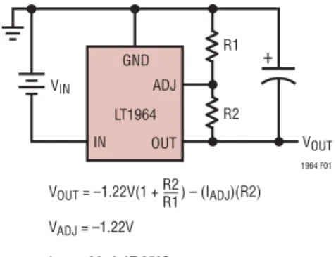
Figure 1. Adjustable Operation
The LT1964 is a 200mA negative low dropout regulator with micropower quiescent current and shutdown. The device is capable of supplying 200mA at a dropout voltage of 340mV. Output voltage noise can be lowered to 30μVRMS over a 10Hz to 100kHz bandwidth with the addition of a 0.01μF reference bypass capacitor. Additionally, the refer-ence bypass capacitor will improve transient response of the regulator, lowering the settling time for transient load conditions. The low operating quiescent current (30μA) drops to 3μA in shutdown. In addition to the low quies-cent current, the LT1964 incorporates several protection features which make it ideal for use in battery-powered systems. In dual supply applications where the regulator load is returned to a positive supply, the output can be pulled above ground by as much as 20V and still allow the device to start and operate.
Adjustable Operation
The adjustable version of the LT1964 has an output volt-age range of –1.22V to –20V. The output voltvolt-age is set by the ratio of two external resistors as shown in Figure 1. The device servos the output to maintain the voltage at the ADJ pin at –1.22V referenced to ground. The current in R1 is then equal to –1.22V/R1 and the current in R2 is the current in R1 plus the ADJ pin bias current. The ADJ pin bias current, 30nA at 25°C, fl ows through R2 out of the ADJ pin. The output voltage can be calculated using
the formula in Figure 1. The value of R1 should be less than 250k to minimize errors in the output voltage caused by the ADJ pin bias current. Note that in shutdown the output is turned off and the divider current will be zero. Curves of ADJ Pin Voltage vs Temperature and ADJ Pin Bias Current vs Temperature appear in the Typical Performance Characteristics section.
The adjustable device is tested and specifi ed with the ADJ pin tied to the OUT pin and a 5μA DC load (unless otherwise specifi ed) for an output voltage of –1.22V. Specifi cations for output voltages greater than –1.22V will be propor-tional to the ratio of the desired output voltage to –1.22V; (VOUT/ –1.22V). For example, load regulation for an output current change of 1mA to 200mA is 2mV typical at VOUT = –1.22V. At VOUT = –12V, load regulation is:
(–12V/–1.22V) • (2mV) = 19.6mV
Bypass Capacitance and Low Noise Performance
The LT1964 may be used with the addition of a bypass capacitor from VOUT to the BYP pin to lower output voltage noise. A good quality low leakage capacitor is recom-mended. This capacitor will bypass the reference of the LT1964, providing a low frequency noise pole. The noise pole provided by this bypass capacitor will lower the out-put voltage noise to as low as 30μVRMS with the addition of a 0.01μF bypass capacitor. Using a bypass capacitor has the added benefi t of improving transient response. With no bypass capacitor and a 10μF output capacitor, a –10mA to –200mA load step will settle to within 1% of its fi nal value in less than 100μs. With the addition of a 0.01μF bypass capacitor, the output will stay within 1% for the same –10mA to –200mA load step (see LT1964-5 Transient Response in the Typical Characteristics section). However, regulator start-up time is proportional to the size of the bypass capacitor.
Higher values of output voltage noise may be measured if care is not exercised with regard to circuit layout and testing. Crosstalk from nearby traces can induce unwanted noise onto the output of the LT1964-X.
1964 F01 GND ADJ IN OUT LT1964 VIN VOUT + R1 R2 VOUT = –1.22V(1 + ) – (IADJ)(R2) VADJ = –1.22V IADJ = 30nA AT 25°C OUTPUT RANGE = –1.22V TO –20V R2 R1
12
1964fb
APPLICATIONS INFORMATION
Output Capacitance and Transient ResponseThe LT1964 is designed to be stable with a wide range of output capacitors. The ESR of the output capacitor affects stability, most notably with small capacitors. A minimum output capacitor of 1μF with an ESR of 3Ω or less is recommended to prevent oscillations. The LT1964 is a micropower device and output transient response will be a function of output capacitance. Larger values of output capacitance decrease the peak deviations and provide improved transient response for larger load current changes. Bypass capacitors, used to decouple individual components powered by the LT1964, will increase the effective output capacitor value.
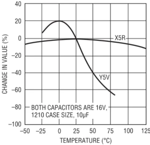
Extra consideration must be given to the use of ceramic capacitors. Ceramic capacitors are manufactured with a variety of dielectrics, each with different behavior across temperature and applied voltage. The most common dielectrics used are specifi ed with EIA temperature char-acteristic codes of Z5U, Y5V, X5R and X7R. The Z5U and Y5V dielectrics are good for providing high capacitances in a small package, but they tend to have strong voltage and temperature coeffi cients as shown in Figures 2 and 3. When used with a 5V regulator, a 16V 10μF Y5V capacitor can exhibit an effective value as low as 1μF to 2μF for the DC bias voltage applied and over the operating tempera-ture range. The X5R and X7R dielectrics result in more stable characteristics and are more suitable for use as the output capacitor. The X7R type has better stability across temperature, while the X5R is less expensive and is avail-able in higher values. Care still must be exercised when using X5R and X7R capacitors; the X5R and X7R codes only specify operating temperature range and maximum capacitance change over temperature. Capacitance change due to DC bias with X5R and X7R capacitors is better than Y5V and Z5U capacitors, but can still be signifi cant enough to drop capacitor values below appropriate levels. Capaci-tor DC bias characteristics tend to improve as component case size increases, but expected capacitance at operating voltage should be verifi ed.
Figure 2. Ceramic Capacitor DC Bias Characteristics
Figure 3. Ceramic Capacitor Temperature Characteristics
DC BIAS VOLTAGE (V) CHANGE IN V ALUE (%) 1964 F02 20 0 –20 –40 –60 –80 –100 0 2 4 6 8 10 12 14 X5R Y5V 16 BOTH CAPACITORS ARE 16V, 1210 CASE SIZE, 10μF TEMPERATURE (°C) –50 40 20 0 –20 –40 –60 –80 –100 25 75 1964 F03 –25 0 50 100 125 Y5V CHANGE IN VALUE (%) X5R
BOTH CAPACITORS ARE 16V, 1210 CASE SIZE, 10μF
Voltage and temperature coeffi cients are not the only sources of problems. Some ceramic capacitors have a piezoelectric response. A piezoelectric device generates voltage across its terminals due to mechanical stress, similar to the way a piezoelectric accelerometer or micro-phone works. For a ceramic capacitor the stress can be induced by vibrations in the system or thermal transients. The resulting voltages produced can cause appreciable
13
1964fb
APPLICATIONS INFORMATION
amounts of noise, especially when a ceramic capacitor is used for noise bypassing. A ceramic capacitor produced Figure 4’s trace in response to light tapping from a pencil. Similar vibration induced behavior can masquerade as increased output voltage noise.
For surface mount devices, heat sinking is accomplished by using the heat spreading capabilities of the PC board and its copper traces. Copper board stiffeners and plated through-holes can also be used to spread the heat gener-ated by power devices.
The following tables list thermal resistance for several different board sizes and copper areas. All measurements were taken in still air on 3/32" FR-4 board with one ounce copper.
Table 1. SOT-23 Thermal Resistance
COPPER AREA BOARD AREA THERMAL RESISTANCE (JUNCTION-TO-AMBIENT) TOPSIDE* BACKSIDE 2500mm2 2500mm2 2500mm2 125°C/W 1000mm2 2500mm2 2500mm2 125°C/W 225mm2 2500mm2 2500mm2 130°C/W 100mm2 2500mm2 2500mm2 135°C/W 50mm2 2500mm2 2500mm2 150°C/W *Device is mounted on topside.
Table 2. DFN Thermal Resistance
COPPER AREA BOARD AREA THERMAL RESISTANCE (JUNCTION-TO-AMBIENT) TOPSIDE* BACKSIDE 2500mm2 2500mm2 2500mm2 40°C/W 1000mm2 2500mm2 2500mm2 45°C/W 225mm2 2500mm2 2500mm2 50°C/W 100mm2 2500mm2 2500mm2 62°C/W *Device is mounted on topside.
The thermal resistance junction-to-case (θJC), measured at Pin 2, is 60°C/W. for the SOT-23 package and is 16°C/W measured at the backside of the exposed pad on the DFN package
Calculating Junction Temperature
Example: Given an output voltage of –5V, an input voltage range of –6V to –8V, an output current range of 0mA to –100mA, and a maximum ambient temperature of 50°C, what will the maximum junction temperature be?
The power dissipated by the device will be equal to:
Figure 4. Noise Resulting from Tapping on a Ceramic Capacitor
LT1964-5 COUT = 10μF CBYP = 0.01μF ILOAD = –200mA VOUT 1mV/DIV 100ms/DIV 1964 F04 Thermal Considerations
The power handling capability of the device will be limited by the maximum rated junction temperature (125°C). The power dissipated by the device will be made up of two components:
1. Output current multiplied by the input/output voltage differential: IOUT • (VIN – VOUT), and
2. Ground pin current multiplied by the input voltage: IGND • VIN
The GND pin current can be found by examining the GND Pin Current curves in the Typical Performance Character-istics. Power dissipation will be equal to the sum of the two components listed above.
The LT1964 series regulators have internal thermal limiting designed to protect the device during overload conditions. For continuous normal conditions the maximum junction temperature rating of 125°C must not be exceeded. It is important to give careful consideration to all sources of thermal resistance from junction to ambient. Additional heat sources mounted nearby must also be considered.
14
1964fb IOUT(MAX) • (VIN(MAX) – VOUT) + (IGND • VIN(MAX))
where,
IOUT(MAX) = –100mA VIN(MAX) = –8V
IGND at (IOUT = –100mA, VIN = –8V) = –2mA so,
P = –100mA • (–8V + 5V) + (–2mA • –8V) = 0.32W The thermal resistance (junction to ambient) will be in the range of 125°C/W to 150°C/W for the SOT-23 package depending on the copper area. So the junction temperature rise above ambient will be approximately equal to: 0.32W • 140°C/W = 44.2°C
The maximum junction temperature will then be equal to the maximum junction temperature rise above ambient plus the maximum ambient temperature or:
TJMAX = 50°C + 44.2°C = 94.2°C
Protection Features
The LT1964 incorporates several protection features which make it ideal for use in battery-powered circuits. In addition to the normal protection features associated with monolithic regulators, such as current limiting and thermal limiting, the device is protected against reverse input voltages and reverse output voltages.
Current limit protection and thermal overload protection are intended to protect the device against current overload conditions at the output of the device. For normal operation, the junction temperature should not exceed 125°C. The output of the LT1964 can be pulled above ground without damaging the device. If the input is left open circuit or grounded, the output can be pulled above ground by 20V. For fi xed voltage versions, the output will act like a large resistor, typically 500k or higher, limiting current fl ow to less than 40μA. For adjustable versions, the output will
APPLICATIONS INFORMATION
act like an open circuit, no current will fl ow into the pin. If the input is powered by a voltage source, the output will sink the short-circuit current of the device and will protect itself by thermal limiting. In this case, grounding the SHDN pin will turn off the device and stop the output from sinking the short-circuit current.
Like many IC power regulators, the LT1964 series have safe operating area protection. The safe area protection activates at input-to-output differential voltages greater than –7V. The safe area protection decreases the current limit as the input-to-output differential voltage increases and keeps the power transistor inside a safe operating region for all values of forward input to-output voltage. The protection is designed to provide some output current at all values of input-to-output voltage up to the device breakdown. A 50μA load is required at input-to-output differential voltages greater than –7V.
When power is fi rst turned on, as the input voltage rises, the output follows the input, allowing the regulator to start up into very heavy loads. During start-up, as the input voltage is rising, the input-to-output voltage differential is small, allowing the regulator to supply large output currents. With a high input voltage, a problem can occur wherein removal of an output short will not allow the output voltage to fully recover. Other regulators, such as the LT1175, also exhibit this phenomenon, so it is not unique to the LT1964 series.
The problem occurs with a heavy output load when the input voltage is high and the output voltage is low. Common situations are immediately after the removal of a short-circuit or when the SHDN pin is pulled high after the input voltage has already been turned on. The load line for such a load may intersect the output current curve at two points. If this happens, there are two stable operat-ing points for the regulator. With this double intersection, the input supply may need to be cycled down to zero and brought up again to make the output recover.
15
1964fb
Information furnished by Linear Technology Corporation is believed to be accurate and reliable. However, no responsibility is assumed for its use. Linear Technology Corporation makes no representa-tion that the interconnecrepresenta-tion of its circuits as described herein will not infringe on existing patent rights.
PACKAGE DESCRIPTION
1.50 – 1.75 (NOTE 4) 2.80 BSC 0.30 – 0.45 TYP 5 PLCS (NOTE 3) DATUM ‘A’ 0.09 – 0.20(NOTE 3) S5 TSOT-23 0302 REV B
PIN ONE 2.90 BSC (NOTE 4) 0.95 BSC 1.90 BSC 0.80 – 0.90 1.00 MAX 0.01 – 0.10 0.20 BSC 0.30 – 0.50 REF NOTE:
1. DIMENSIONS ARE IN MILLIMETERS 2. DRAWING NOT TO SCALE
3. DIMENSIONS ARE INCLUSIVE OF PLATING
4. DIMENSIONS ARE EXCLUSIVE OF MOLD FLASH AND METAL BURR 5. MOLD FLASH SHALL NOT EXCEED 0.254mm
6. JEDEC PACKAGE REFERENCE IS MO-193 3.85 MAX
0.62 MAX
0.95 REF
RECOMMENDED SOLDER PAD LAYOUT PER IPC CALCULATOR
1.4 MIN 2.62 REF
1.22 REF
S5 Package 5-Lead Plastic TSOT-23
(Reference LTC DWG # 05-08-1635) DD Package 8-Lead Plastic DFN (3mm × 3mm) (Reference LTC DWG # 05-08-1698) 3.00 ±0.10 (4 SIDES) NOTE:
1. DRAWING TO BE MADE A JEDEC PACKAGE OUTLINE M0-229 VARIATION OF (WEED-1) 2. DRAWING NOT TO SCALE
3. ALL DIMENSIONS ARE IN MILLIMETERS
4. DIMENSIONS OF EXPOSED PAD ON BOTTOM OF PACKAGE DO NOT INCLUDE MOLD FLASH. MOLD FLASH, IF PRESENT, SHALL NOT EXCEED 0.15mm ON ANY SIDE 5. EXPOSED PAD SHALL BE SOLDER PLATED
6. SHADED AREA IS ONLY A REFERENCE FOR PIN 1 LOCATION ON TOP AND BOTTOM OF PACKAGE
0.38 ± 0.10
BOTTOM VIEW—EXPOSED PAD 1.65 ± 0.10 (2 SIDES) 0.75 ±0.05 R = 0.115 TYP 2.38 ±0.10 (2 SIDES) 1 4 8 5 PIN 1 TOP MARK (NOTE 6) 0.200 REF 0.00 – 0.05 (DD) DFN 1203 0.25 ± 0.05 2.38 ±0.05 (2 SIDES)
RECOMMENDED SOLDER PAD PITCH AND DIMENSIONS 1.65 ±0.05 (2 SIDES) 2.15 ±0.05 0.50 BSC 0.675 ±0.05 3.5 ±0.05 PACKAGE OUTLINE 0.25 ± 0.05 0.50 BSC
16
1964fb
Linear Technology Corporation
1630 McCarthy Blvd., Milpitas, CA 95035-7417(408) 432-1900 ● FAX: (408) 434-0507 ● www.linear.com © LINEAR TECHNOLOGY CORPORATION 2001
LT 0708 REV B • PRINTED IN USA
RELATED PARTS
PART NUMBER DESCRIPTION COMMENTS
LT1120 125mA Micropower Low Dropout Regulator with Comparator and Shutdown
Includes 2.5V Reference and Comparator, VIN: 3.5V to 36V, IQ = 40μA,
N8 Package
LT1121 150mA Micropower Low Dropout Regulator VIN: 4.2V to 30V, IQ = 30μA; ThinSOT, S8 and MS8 Packages
LT1129 700mA Micropower Low Dropout Regulator VIN: 4.5V to 30V, IQ = 50μA; DD and S8 Packages
LT1175 800mA Negative Low Dropout Micropower Regulator VIN: 4.5V to 20V, IQ = 45μA, 0.26V Dropout Voltage, S8 and
ThinSOT Packages
LT1611 Inverting 1.4MHz Switching Regulator –5V at 150mA from 5V Input, ThinSOT Package
LT1761 Series 100mA, Low Noise, Low Dropout Micropower Regulators VIN: 1.5V to 20V, I Q = 20μA, 20μVRMS Noise, ThinSOT Package
LT1762 Series 150mA, Low Noise, LDO Micropower Regulators VIN: 1.5V to 20V, I Q = 25μA, 20μVRMS Noise, MS8 Package
LT1763 Series 500mA, Low Noise, LDO Micropower Regulators VIN: 1.5V to 20V, I Q = 30μA, 20μVRMS Noise, S8 Package
LT1764A 3A, Low Noise, Fast Transient Response LDO VIN: 1.5V to 20V, 40μVRMS Noise; DD and T5 Packages
LT1931/LT1931A Inverting 1.2MHz/2.2MHz Switching Regulators –5V at 350mA from 5V Input, ThinSOT Package
LT1962 300mA, Low Noise, LDO Micropower Regulator VIN: 1.5V to 20V, I Q = 30μA, 20μVRMS Noise, MS8 Package