I. Luk’yanchuk,1, 2 A. Sen´e,1 and V. M. Vinokur3
1University of Picardie, Laboratory of Condensed Matter Physics, Amiens, 80039, France 2Landau Institure for Theoretical Physics, Moscow, Russia
3Materials Science Division, Argonne National Laboratory, 9700 S. Cass Ave, Argonne, IL 60439, USA
We construct a comprehensive theory of the electrodynamic response of ferroelectric ultra-thin films con-taining periodic domain textures (PDT) with 180◦
polarization-oriented domains. The focal point of the theory is the negative-capacitance phenomenon which naturally arises from the depolarization field induced by PDT. We derive frequency-dependent dielectric permittivity related to the PDT dynamics across the entire frequency range. We find the resonance mode of domain oscillations in the THz spectral band and the singular points in the phase of the reflected THz beam that are intimately related to the negative capacitance. Our findings provide a platform for the THz negative capacitance-based optics of ferroelectric films and for engineering the epsilon-near-zero plasmonic THz metamaterials.
INTRODUCTION
Functional properties of ferroelectric films and superlattices are drastically different from those of the bulk materials. Ex-tensive experimental [1–6] and theoretical [7–13] studies re-vealed new physics that emerges from the periodic domain textures (PDT) stabilized by the strains and the depolarization fields. One of the most striking features of the PDT is the man-ifest of the negative capacitance [14], the phenomenon that has been a subject of an intense recent attention [15–20]. The interest is motivated by both, its fundamental importance, and by its high potential for technological applications, in partic-ular, as a platform for novel low-dissipation field-effect tran-sistors.
Another facet of emergent functionalities of ferroelectric films arises due to the strain-tunability of their multiscale spontaneous polarization dynamics that provides a wide range of operational frequencies from a few kilohertz to tens tera-hertz (1 THz=1012Hz). The spectral band 104Hz−0.3 THz is covered by the relaxation dynamics of the domain walls (DWs) and polar clusters. The far-infrared spectral region of 3−30 THz is governed by the soft-mode vibrations of the polar ions. Recent studies suggested that oscillations of do-main walls (DW) in PDT occur in the frequency window of 0.3 −3 THz [21–23], i.e within the least studied frequency range, referred to as a THz gap.
Our work steps into the breach and demonstrates that the resonant behavior of oscillations of PDT is the collective ef-fect similar to the standard plasmonic excitations in metals. We find that this effect is governed by the stiffness of depo-larization field and is a consequence of the negative capaci-tance. We calculate the electrodynamic response of PDT and find the frequency dependence of the effective dielectric per-mittivity. We investigate the THz optics of the PDT structure and demonstrate the existence of the topologically protected phase-singular points of the absolute darkness in the Fresnel reflection coefficient. These points are a fingerprint of the neg-ative capacitance phenomenon.
Formation of the PDT lowers the energy of the depolar-ization field induced by surface depolardepolar-ization charges that
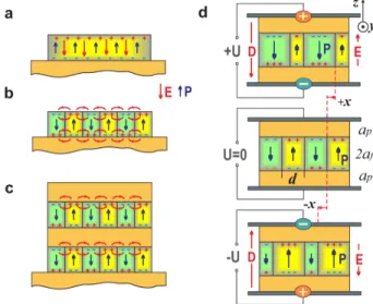
FIG. 1. Formation and dynamics of the periodic domain texture (PDT). (a) A single-domain state, the ferroelectric polarization and the depolarization field are shown by the blue and red arrows, re-spectively. The depolarization field traverses across the film. (b) The PDT with the alternating 180◦
polarization domains. The depolar-ization field is confined to the surface of the film. (c) A sketch of the ferroelectric-paraelectric superlattice with PDT. (d) The change of the PDT upon varying of the applied field in the ferroelectric-paraelectric system.
appear at polarization termination points. Had the polariza-tion maintained the same direcpolariza-tion throughout a slab, see Fig.1a, the electrostatic energy stored by the depolarization field would be proportional to the volume of the whole system hence huge. Splitting the system into the PDT implies that the surface depolarization charges form stripes of alternating signs. As a result, the depolarization field becomes restricted to the near-surface shell, see Fig.1b, hence drastically dimin-ishing the related electrostatic energy. Although predicted al-ready in earlier works by Landau [24,25] and Kittel [26] in the context of ferromagnetic systems, the PDT in ferroelectric films has long been viewed as unlikely until the recent direct experimental evidences for equilibrium 180◦ stripe domains in strained ferroelectric thin films of PbTiO3(PTO) deposited
the surfaces and flowing between the electrodes, thus compen-sating the depolarization field inside the ferroelectric. As a result, the depolarization energy is nullified, the domain walls would creep away, and the mono-domain state stabilizes. This tendency of a ferrolecric with the PDT to self-generating the charge at its surfaces can be expressed via attributing to the ferroelectric slab anegativecapacitance. One should bear in mind, however, that in reality, the slab that is not linked to the electrodes, maintains the PDT since charges cannot propagate across the dielectric and the charge redistribution described above would not occur.
It is the overscreeing effect due to the depolarization field that lies in the origin of the negative capacitance. The compo-nent of the depolarization field penetrating the bulk of the fer-roelectric slab from the surface is opposite to the applied field and exceeds it by the absolute value. As a result, the total field inside the slab is counter-directed to the induced polarization. Hence the dielectric permittivity is negative. Writing down the coupled PDT equations of motion and Maxwell equations, we derive the dynamic frequency-dependent dielectric permittiv-ity of the ferroelectric films and superlattices containing PDT across the entire frequency range and find the corresponding resonance mode. We show that its emergence is intimately related to the low frequency negative dielectric permittivity.
RESULTS Negative capacitance
We start the description of the domain electrodynamics with the static limit, and show that PDT in response to the applied field develops the fascinating negative dielectric per-mittivityεf and, accordingly, the negative capacitance,C =
ε0εfS/(2af), of the ferroelectric layer of surface area S and thickness 2af. We further demonstrate that the negative static εf of the PDT is a key element for striking arising of the reso-nance mode of DWs oscillations at THz frequencies.
The applied field is characterized by the inductionDthat conserves all across the system, see Fig.1d, and generates the net polarization of the ferroelectric layer,P k z(the electro-static fields in the ferroelectric slab with domains are macro-scopically averaged). In our ferroelectric film the induction is related to the electric field through
D=ε0εkE+Pdw. (1)
The contributionPdw stems from the motion of the domain
σ=Pdw. Thus the depolarization fieldEdep =−(ε0εk)−1Pdw penetrates the bulk of the slab and is directed opposite to the applied field D. This field, together with the driving field
ED=(ε0εk)−1Dwhich would have settled down if DWs were immobile, contributes to the total field,E=ED+Edep. Hence the sign of the system’s dielectric permittivity, which is de-fined as
εf =ε0D
E, (2)
depends on the relative magnitude of the oppositely oriented
EDandEdep.
Making use of the relation (1), one obtains εf= εkD
D−Pdw
. (3)
To deriveεf, we have to know how the polarization related to the DW displacement depends on the applied fieldD. The calculations presented in the Appendix result in
εf=εk− πς 4 ln 2 ε⊥ εk !1/22 af d εk, (4)
where the first term stems from the positive intrinsic contribu-tion ofED, whereas the second, the negative one, is generated by the depolarizing fieldEdep, reflecting the effect of the mov-ing DW. The depolarizmov-ing term outweights the intrinsic term, hence the negative dielectric permittivity settles, provided the film thickness, 2afexceeds the domain width,d. The equilib-rium value ofdcan be either taken from the experiment [1,4] or estimated by the Landau-Kittel square root law [24–26] specifically adapted for ferroelectrics in [7,11,27],
d'
q
3.53 ε⊥/εk1/2ςδ·2af. (5) The resulting typical domain configuration for PTO films is shown in Fig.1b. The DW thickness,δ, is about 1 nm [28]. In the above formulasς = 1+εp/ εkε⊥1/2, and the values of intrinsic permittivities along and across the polarization direction,εk, ε⊥, and of paraelectric layer, εp, are specified below; in the experimental range 1 6 ς 6 4. If the sand-wiching paraelectric layers possess different permittivities,ε+p andε−1
p , the effective parameterςeff is defined by the relation ς−1 eff = 1 2 h ς−1(ε+ p)+ς−1(ε−p) i
. In particular, if the ferroelectric film is deposited on the metallic substrate so thatε−
p =1 and ε+
p =∞, one hasςeff'2. The polarization profile in this case can be obtained by the image method.
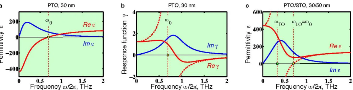
FIG. 2. Dynamical properties of the PDT. Real and imaginary parts of the frequency-dependent response are shown by red and blue colors respectively. Dashed lines depict the behavior of the system in the absence of dissipation. (a) Dielectric permittivity of the 30 nm thick film of the PTO. (b) Response function, defined asPdwω=γ(ω)Dω, for the same film. (c) Dielectric permittivity for either the 30/50 nm sandwich of
the PTO/STO layers, or for the equivalent superlattice.
DW oscillations
To quantify the electromagnetic behavior of PDT, we de-rive the dynamic response functionγ(ω), defined by the rela-tionPdwω=γ(ω)Dω, for the periodic structure of the domain
stripes aligned along they-axis which forms in the ferroelec-tric layer. The polarization axiszis perpendicular to the film plane, while the in-plane DW motion occurs along thex-axis, the indexω indicates the Fourrier transforms of the respec-tive quantities. We neglect the longitudinal DW fluctuations which can broad the resonance peak [29].
In the harmonic oscillator approximation [30] the driven dynamics of DWs is given by
µ..x(t)+ηx.(t)+kx(t)=2PsED(t), (6) where x is the coordinate of alternating DW displacements (Fig.1d), the coefficientsk,µandηare calculated per unit of DW area, and 2PsED(t) is the pressure due to the induction-induced driving field forcing DW to move to flip the surround-ing spontaneous polarization from−Psto+Ps.
Equation (6) presumes that the DW is rigid and atomically narrow. However, in the tens-nanometer-thin films the DW broadens significantly due to depolarization effects in the large range of temperatures (yet the effective thickness of the DWs remains smaller then the distance between them as long and the model holds). The broadening is especially pronounced on approach to the film surface [13] and upon the DW dis-placement the polarization reverses first at the surface and then propagates into the interior of the film [21]. As a result of the DW broadening, the underlying pinning potential for the DW due to the periodic atomic structure gets essentially reduced and becomes relevant only at low temperatures.
The stiffnesskis of a purely electrostatic origin and, there-fore, is not too sensitive to the explicit shape of DW. We cal-culate it as a coefficient at the restoring force that pushes the domain walls back in order to reduce the depolarization field,
Edep=−∆Ps/ε0=−2(x/ε0d)Ps, arising upon the displacment of DW from the equilibrium. This field is induced by the
ex-tra depolarization surface charges,σ =±∆Ps, appearing due to the spontaneous polarization excess,∆Ps =2(x/d)Ps, and is directed antiparallel to∆Ps. We evaluate the depolariza-tion energy of the system as the electrostatic energy of the dielectric slab with permittivityεk and with surface charges σ = 2(x/d)Psas W =
2afσ2/2ε0εk
S, where S is the sur-face area. The corresponding energy per unit area of the dis-placed DW isw=(d/2S af)W. Relating it with the harmonic oscillator stiffness energykx2/2, we find
k= 4P 2 s ε0εkd g, g'1−4 ln 2 πς εk ε⊥ !1/2 d 2af . (7)
The factorg≤1, calculated in the Appendix, makes the above qualitative consideration more precise, taking into account the non-uniform part of the depolarization field near the surface caused by the stepwise distribution of the depolarization sur-face charges. As follows from (7) in very thick samples, these corrections vanish andg→ 1. In realistic cases that we con-sidered here, namely, the PTO films with 2af '10−30 nm, it varies from 0.4 to 0.9.
The effective DW mass,µ, and the viscosity,η, in Eq. (6) are related to the motion of the material-constituent polar ions during the displacement of the DWs [31] and with the piezo-electric effect of the time-varying depolarization field [30]. The magnitude ofµwas calculated inab-initiosimulations of DW dynamics in the sub-THz range [21]. We propose an in-terpolation formulaµ[kg/m2]'1.3√2af[nm]×10−9, which fits well the numerical result. Viscosity,η, is expressed via damping factor of DW motion,Γ =η/µ. Since the consistent theory forΓis not available, we chose the one that appears in the measurements of the soft-mode relaxation of polar ions.
THZ resonance
In what follows we calculate the complex dynamic permit-tivity of PDT,εf(ω). The resulting plots of the real,<εf(ω),
ω0−ω −iΓω µdε0εk
where the characteristic oscillation frequency is the usual ω0=(k/µ)1/2withkandµrelated to the system parameters as discussed above. When deriving Eq. (8), we took into account thatPdwω=2Ps(xω/d)zandDω=ε0εkEDω.
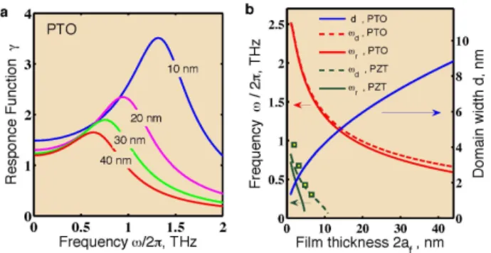
Shown in Fig.2b are the real and imaginary parts ofγ(ω) for our sample exhibiting a characteristic Lorentzian-type form. The latter is a legacy of a singularity at ω0, which would have been exhibited by a system without the dissipa-tion, illustrated by the dashed lines. The emergence of the resonance response to the applied field is clearly demonstrated by the frequency dependencies of the absolute value of the response function, |γ(ω)|, for different film thicknesses, see Fig.3a, and reaching its maximum at the resonance frequency ω2
r =ω20−Γ
2/2. The dependence ofωrupon the film thick-ness, 2af, is shown in Fig.3b. Shown by the blue line in the same panel is the Landau-Kittel dependence of the domain width,d, on the film thickness given by Eq. (5) .
Equation (8) enables optimization of the materials parame-ters and the film thickness to make sure thatωr falls within the desired THz frequency range. In particular, for the strained films of PTO with the high spontaneous polariza-tion, Ps ' 0.65 C m−2, see [32], relatively low permittivities εk ' 100,ε⊥ ' 30, soft mode damping factorΓ '20 cm−1 (0.6 THz) [33] and µ defined as above, the resonance fre-quencyωrdecreases and spans the range from 1.5 to 0.75 THz when 2af increases from 10 to 40 nm. We find the damping frequency,ω2d =ω20−Γ2/4, of the attenuated oscillations of domains in PTO, x(t) = x0e−(Γ/2)tsinωdt, which is slightly larger then ωr, see Fig.3b. Remarkably, our formulas per-fectly describe the results of ab-initio simulations of DWs oscillations in PZT free-standing ultrathin films [21]. The calculated damping frequency, ωd, is shown by the dashed line in the Fig.3b, the symbols display the results of simu-lations. Here we used the following parameters for PZT:Ps' 0.40 C m−2[32],εk, ε⊥'350,Γ'27cm−1(0.8 THz) [34] and the same value for DW mass,µ. At the same time, the res-onance frequency of PZT, ωr, drops rapidly with the thick-ness and vanishes above 4 nm. The data in this paragraph are given for ceramic samples. The values for strained films can be slightly different.
Making use of the relationγ(ω)=1−εk/εf(ω) that follows directly from Eq. (1), we obtain the dynamic permittivity of a ferroelectric layer εf(ω)= εk 1−γ(ω) =εk ω2 0−ω 2−iΓω 1−g−1ω2 0−ω2−iΓω , (9) = 0 f 0 =
This behavior of PDT permittivity resembles that of a metal, having the negative real part of permittivity below theplasma
frequency at which it becomes equal to zero. Accordingly,
this will lead to the plasma resonance atω =ω0in a PDT as a response to the driving fieldD.
The discovered resonance mode gives rise to the Drude-Lorentz frequency response of a biased capacitor consist-ing of the ferroelectric layer (of thickness 2af) sandwiched between paraelectric buffer layers (of thickness ap and per-mittivity εp each). The same response appears in 2af/2ap ferroelectric-paraelectric superlattice. The effective permittiv-ity, calculated for the system of in-series capacitors,ε−1
tot(ω)= αpε−1p +αfε−1f (ω), results from the interplay of the positive, paralectric, and negative, ferroelectric, contributions and re-mains positive at small ω. Here αp = ap/(ap +af) and αf = af/(ap+af) are the relative weights of the respective layers. That it is the paraelectric contribution that dominates the behavior of the effective permittivity atω = 0, is inher-ently related to the very emergence of the domains. Namely, it is related to the fact that the thickness of the paraelectric buffer,ap, is larger then the domain width,d, and thus domain depolarization stray fields do not interact with electrodes [35]. The frequency dependence of theεtot(ω) for PTO/STO 30/50 nm system is shown in Fig.2c. One sees (the detail of cal-culations are given further) that<εtot(ω) maintains a
posi-FIG. 3. Resonance in the PDT. (a) Resonance behavior of the am-plitude of the response function|γ(ω)|for different film thickness of the PTO. (b) Dependencies of the domain resonance frequency,ωr,
of the damping frequency,ωd, and of the domain width,d, upon the
film thickness. The solid red line stands forωrof the PTO, the dashed
red line showsωdof the PTO. The solid and dashed green lines show ωrandωd, respectively, for PZT. Green square symbols display the
results of theab-initiosimulations for the PZT [21]. The blue solid line displays the behavior of the domain width,d.
tive value for low frequencies and reflects the presence of the oscillatory mode at ω slightly less thenω0. As before, the dashed line depicts the behavior of<εtot(ω) in the absence of dissipation. We thus introduce a new metamaterial operating in the THz frequency-rangeεtot(ω) tunable by the variation of ratio 2af/2ap.
Optics
The effective permittivity of a ferroelectric/paraelectric lay-ered system is calculated asε−1
tot(ω) =αpε−1p +αfε−1f (ω) and can be conveniently written in a standard form:
εtot(ω)=ω 2 LO−ω 2−iΓω ω2 TO−ω2−iΓω εtot(∞), (10) where the characteristic frequencies ωLO, ωTO are the
ana-logues of the longitudinal and traversal oscillation frequen-cies in the polar mode spectroscopy. The former one, is the DW oscillation frequency, ωLO = ω0. The latter frequency
can be obtained from the relationω2
TO/ω
2
LO = εtot(∞)/εtot(0)
that is the analog of the Lyddane-Sachs-Teller relation. Here ε−1 tot(0) =αpε −1 p +αfε −1 f andε −1 tot(∞)=αpε −1 p +αfε −1 k . Equa-tion (10) describes the dispersion curve in Fig.2c. It clearly shows that the obtained PDT resonance mode freezes out when the frequency exceedsω0and what is left are the molec-ular vibrations including the polar soft mode oscillations.
The derived dispersion relation for the dielectric permittiv-ity provides a foundation for the description of the THz op-tical properties of a ferroelectric film with PDT, in particu-lar, for finding its complex refraction index, n(ω) = √ε(ω). This enables to devise an approach for inferring the reso-nance properties and negative permittivity effects from the op-tical measurements in the sub(THz) frequency band. Impor-tantly, in the systems that we address, the typical thicknesses of the ferroelectric layer, 2af '10÷40 nm and the PDT pe-riod, 2d, are both less then the wavelength of THz radiation, λ'1÷0.15 mm for 0.3÷2 THz. Hence the THZ wave will interact with the system hosting the PDT as with an ultra-thin dielectric film endowed with the anisotropic dielectric permit-tivity, the latter having the in- and out of plane componentsε⊥ andεf(ω) respectively.
Reflection
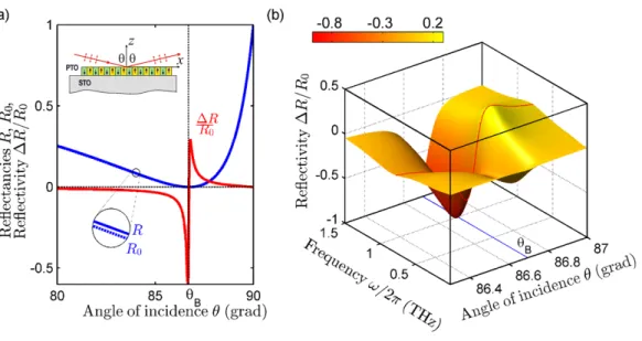
We consider the situation where the incident THz beam gets reflected from the dielectric substrate, STO, with dielectric permittivityεp =300+10iin the sub-THz frequency range, passing twice through the PTO ferroelectric film with PDT. To ensure the interaction of the beam with the PDT polariza-tion, the electric field of the light should be confined to the plane of incidence, hence the p-wave polarization geometry should be used. The experimental setup is shown in the inset in Fig.4a. The calculated reflectance,R, of such a system is
shown in the main panel of Fig.4a as function of the angle of incidence,θ, by the solid blue line. The plot illustrates a typical p-wave reflectance with the amplitude that nearly van-ishes in the vicinity of the Brewster angle of the substrate, θB ≈ arctan
<εp1/2 ' 86.7◦. For comparison, shown in Fig.4a by the blue dashed line is also the net contribution of the substrate. Note that because of the very small thick-ness of the film, it is practically indistinguishable from the re-flectance of the whole system. The difference between them, ∆R = R0 −R ' 10−3, is seen only under a magnification. Thus, to ensure the efficient filtering of the resonance PDT signal from the background substrate contribution, one has to focus instead on the relative variance of the signals difference, ∆R/R0, usually referred to as to reflectively and used to detect the tiny molecular mono-layers adsorbed on the substrate [36], see Fig.4.
An advantage of using the reflectivity is that the value of the substrate reflectance,R0, almost vanishes atθBand the use
of the ratio∆R/R0 unravels the net contribution of the ultra-thin filmper se. Shown by the solid red line, the reflectivity of our system does experience the drastic variation of about unity and clearly displays the Lorentz-like spike in vicinity ofθB. This spike is a fingerprint of the PDT resonance and
can be used for its experimental identification. The complete qualitative behavior of the resonance feature is illuminated by the three-dimensional color plot of∆R/R0, as function of the frequency and the angle of incidence (Fig.4b). The Lorentz-spike sharp behaviour gets smoothed upon the deviation from the resonance frequency.
The reflectancies R and R0 are calculated as a square of the magnitude of the corresponding Fresnel reflection coeffi -cients,R = |r123p |2 andR
0 = |r p 13|
2. Here index p refers to the beam polarization and indices 1, 2, and 3 correspond to the ordering of the media: the air, the film, and the substrate, respectively.
The Fresnel reflection coefficient of the substrate-deposited film is given by the expression [36]
r123p = r p 12+r p 23e 2iβ 1+r12pr23pe2iβ, (11) where ri jp = εjξi−εiξj εjξi+εiξj , i,j=1,2,3 (12)
are the generalized Fresnel reflection coefficients between two adjacent media andβ=2π2af/λ
ξ2is the phase shift of the electromagnetic wave after a single pass through the film. The generalized indices of refraction,ξi, are defined via the angle of incidence,θ1, and dielectric permittivities of the media,εi, as ξ1= √ ε1cosθ1, ξ2= ε⊥− ε⊥ ε2 ε1sin2θ1 !1/2 (13) ξ3 = ε3−ε1sin2θ1 1/2 . (14)
FIG. 4. Reflection characteristics of the PDT. The p-polarized THz beam reflects from the 2af ' 30 nm-thick PTO film deposited on the
STO dielectric substrate. (a) The dependence of the reflectance of the film on the substrate,R, and the dependence of the net reflectance of the substrate,R0, on the incidence angle,θ, calculated at the PDT oscillation frequencyω0/2π' 0.75 THz are shown by the blue solid
and dashed lines correspondingly. The difference between the both is tiny, |∆R| = |R0−R| . 10−3, and in the figure scale is seen only
under magnification. At variance, the reflectivity,∆R/R0, experiences the drastic variation of about unity and clearly displays the Lorentz-like
spike at the Brewster angleθB '86.7◦
whereR0 almost vanishes. This spike is a fingerprint of the PDT resonance and can be used for its
experimental identification. The inset shows the geometry of the experiment. (b) The 3D color plot of the reflectivity,∆R/R0, as function of
the frequency and the incident angle in the immediate vicinity of the Brewster angle,θB, marked by thin blue line. The red line corresponds to
the Lorentz-spike-like reflectivity behaviour at the PDT oscillation frequency,ω0. This spike smoothens upon the deviation fromω0.
FIG. 5. The complex Fresnel reflection coefficient,r123p , of the PDT. (a) The 3D color plot of the phase and the amplitude ofr123p as function of the frequency,ω, and the angle of incidence,θ, for the 2af '30 nm-thick PTO film deposited on the transparent substrate. The substrate
permittivityεp =300 is real with the vanishingly small imaginary part. Two topologically protected phase singularity dark points, at which |r123p |=0, appear in the vicinity of the Brewster angleθBat frequencies whereεf =0 and whereεf' −
√
εpε⊥. These singular points and the
inversion of the phase rotation between them that came out in blue is the fingerprint of the negative permittivity in the low-frequency region atω < ω0. (b) The same as (a) but for the finite transparency STO substrate withεp =300+10i. The singular phase dark points merge and
annihilate. The color legend refers to both panels (a) and (b). The color maps of the phase distribution are shifted down from|r123p |=0 plain for convenience.
While the refraction indicesξ1andξ3represent the customary properties of the air,ε1 =1, and substrate,ε3 =εpendowed with the isotropic permittivities, the targeted electrodynamic response of PDT with negative capacitance is encoded in the anisotropic refraction indexξ2that is deduced from [37]. The latter grasps both the transversal permittivity of the film,ε⊥, and the effective longitudinal permittivity of PDS,ε2=εf(ω). The described approach identifies the PDT resonance be-havior via detecting the characteristic Lorentz-like spike fea-tures in the angular and frequency dependencies of the re-flectance. However, the developed theory of the electro-magnetic response equips us with the extraordinary more ad-vanced technique. Namely, the resonance point ω0 where εf(ω) changes the sign, is found, with the great precision from the phase map of the Fresnel coefficientr123p . The latter (unlike the real-value reflectanceR = |r123p |2, where the phase infor-mation is lost) is a complex quantity which is measured, for example, by the phase-resolved ellipsometry technique [38].
To develop a feasible protocol for observation of the fre-quency domain endowed with negativeεf let us describe the dependencer123p (θ) near the Brewster angle in the system with the ideally transparent substrate with=εp = 0. If the film were absent, the Fresnel coefficient would have been real and changed the sign upon passing zero atθ=θB. Placing the film
on the substrate, gives the contribution, albeit very small, that pullsr123p into a complex plane, where the trajectory r123p (θ) circumflexes the zero from the positive- to negative semi-axis acquiring the phase±π. Equations (11)-(14) offering a full description of the electromagnetic response show that the di-rection (clock- vs. anticlock-wise) of the phase rotation is de-termined by the sign of εf. The frequency ω0 at which εf changes the sign corresponds, therefore, to a particular point in the (θ, ω)-plane where phase acquires a factor of 2πwhen making a close loop around it, and the Fresnel coefficient,
r123p , vanishes. These zeros of the complex function,r123p (θ, ω), where the intensity of the reflected light is zero are often called ‘points of absolute darkness’ [39]. They are stable with re-spect to small variations of parameters hence topologically protected, and we refer to them as to topological darkness points.
Figure5a displays the 3D color plot of the phase and am-plitude of the Fresnel reflection coefficient,r123p , of the PDT in the 30nm PTO film as a function of an incident angle and frequency for the case of transparent substrate withεp =300, derived from Eqs. (11)-(14). Two topological dark points re-sulting from the negative permittivity are clearly visible at the manifold depictingr123p (θ, ω). The higher-frequency point A corresponds to the discussed above sign change of εf. The second, lower-frequency one, appears when εf ' −√εpε⊥. This manifestly illustrates the topological protection effect: the topological darkness points are not smoothed but merely shifted by dissipation. Figure5b shows the the same phase plot for the PTO on a real substrate STO withεp=300+10i. One sees that if the dissipation is sufficiently large, the dark-ness points merge and cease to exist, i.e. the sharp Brewster-angle singularities in the phase plot get smoothened.
The obtained results and recent measurements of the nega-tive capacitance in PDT [14] open a new area of research in the field of the THz optics in ferroelectric materials. Exciting op-portunities open in the area of the plasmonic epsilon-near-zero (ENZ) metamaterials having the unique property that the elec-tromagnetic wave propagates with almost no phase advance. Although such materials have been made artificially in the mi-crowave, visible and far-infrared spectral ranges [40], the en-gineered ENZ structures in the THz spectral range have not been explored so far.
Acknowledgments
The work was supported by the U.S. Department of En-ergy, Office of Science, Materials Sciences and Engineering Division (VV) and European FP7-MC-ITN-NOTEDEV and H2020-MC-RISE-ENGIMA actions (IL).
APPENDIX
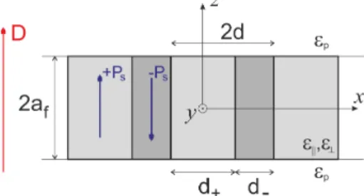
Calculations of the electrostatic properties of PDT in the ap-plied fieldDgeneralize the zero-field Landau-Kittel calcula-tions of PDT given in the textbook [25] in application to mag-netic domains. The geometry of the system is shown in Fig.6. Thex-axis is directed along the PDT texture, they-axis is par-allel to the domains and thez-axis is directed across the film. Since the polarization distribution does not change along the y-axis, the problem is reduced to the 2D one in thexz-plane. In the external field the up- and down-oriented polarization domains have different widths,d+ andd−, the field-induced polarization due to DW motion being expressed via the field dependence of the asymmetry factorη = (d+−d−)/2d as
Pdw = η(D)Ps, with 2d = d++d− being the period of the structure. Following the relation (3) we express the dielectric permittivity of the PDT as:
εf = εk
1−(η(D)/D)Ps
. (15)
The linear dependenceηonDis found by minimization of the electrostatic energy of the system, consideringηas variation parameter.
FIG. 6. The geometry of the system.
We start with the derivation of the spacial distribution of the electric fields inside the ferroelectric (f) and paraelectric (p)
(εk∂2z+ε⊥∂2x)ϕ
(f)=0, (16) εp(∂2z+∂2x)ϕ(p) =0.
The boundary conditions for the potential at the interfaces are fixed by the chargesσ±(x):
ε0εk∂zϕ(f)−ε0εp∂zϕ(p) =±σ±(x), (17) ϕ(f)=ϕ(p).
System (16) with boundary conditions (17) is solved by the Fourier-series expansion method, taking into account that
σ±(x)=±ϑ(x)Ps=± η+ ∞ X n=1 pncosqnx Ps (18) withqn=πn/dand pn= 4 πnsin 1+η 2 πn (19)
After straightforward calculations we obtain:
ϕ(f)= z af ϕ0+Ps ∞ X n=1 ψn sinh pε⊥/εkqnz sinh pε⊥/εkqnaf cosqnx, (20)
whereϕ0=∓ ε0εk (D−ηPs)afis the average value of the potential at the upper/lower surface of the ferroelectric slab, and ψn= pn qnε0 √ ε⊥εk coth pε⊥/εkqnaf +qnε0εp . (21)
The electrostatic energy of the system can be calculated as the integralP
± R
dxR ϕ(x)
z=±afdσ±(x) over the surfaces of
the ferroelectric layer. The integration over σ± reflects the self-consistent adiabatic charging of the surfaces, driven by the self-polarization of the system from the paraelectric state, until the state with the equilibrium spontaneous polarization,
±Ps, is achieved inside domains.
Taking into account the dependicies given by (20) ofϕ(x) andσ±(x) on Ps we calculate the energy per unit length of PDT ( here the factor 2 is because of the two 2 sides of the slab): Fel=2 1 2d Z 2d 0 dx Z Ps 0 ϕ(x,P0 s)z=afϑ(x)dP 0 s=2 Z Ps 0 dP0s ϕ0(P 0 s)η+ 1 2P 0 s ∞ X n=1 pnψn (22) = 2af ε0εk 1 2P 2 sη2−DPsη ! +P2s ∞ X n=1 8d π3n3 sin2(1+η)πn/2 ε0 √ε ⊥εkcoth πnpε⊥/εkaf/d +ε0εp ,
In the experimentally relevant limit pε⊥/εkaf/d 1, Eq. (22) is simplified as:
Fel= 2af ε0εk 1 2P 2 sη 2−DPsη ! +π3ε 8 0ς √ ε⊥εk d f(η)P2s, (23) where f(η)= ∞ X n=1 n−3sin2(1+η)πn 2 η→0 ' 7 8ζ(3)− ln 2 4 (πη) 2. (24)
Minimization of (23) with respectηgives: η= D Ps 1−4 ln 2 πς εk ε⊥ !1/2 d 2af −1 . (25)
Finally, making use (15) we obtain the dielectric permittivity of the PDT (4).
The DW displacements in PDT shown in Fig.1d are given by±x = ±ηd/2. Equating the stiffness energy of the DW displacement, 2af·kx2/2, to (23) (taken in harmonic approx-imation atD=0 and multiplying byd, i.e. using the energy per a single DW), we obtain the expression for the stiffness coefficient,k, (7).
Note that the expression (4) can also be derived from the formulas given in [8] by expressing the ratioPa/Uin Eq. (31) of [8] via the ratioR/S defined in their Eq. (25). The Landau-Kittel formula (5) for the domain width,d, is obtained by min-imization ofFel+Fdwenergy with respectdatη =0. Here
Fdw =(af/d)wdw is the domain wall energy, calculated per unit length of PDT andwdwis the surface energy of DW. The spatial distribution of the electric and polarization fields in the
p- and f- slabs are found from (20) as:E(p,f) =(E(xf),E (f) z )= −∇ϕ(p,f), P(p) = ε 0 εp−1 E(p), P(f) = P(xf),P (f) z where P(xf)=ε0(ε⊥−1)E (f) x ,P (f) z =ε0 εk−1E (f) z +ϑ(x)Ps. For the very thin films the field lines ofP((r) form the closed loops, resembling the alternating vortex-antivortex patterns [6]
[1] S. K. Streiffer, J. Eastman, D. Fong, C. Thompson, A. Munkholm, M. R. Murty, O. Auciello, G. Bai, and G. Stephenson, Phys. Rev. Lett.89, 067601 (2002).
[2] D. D. Fong, G. B. Stephenson, S. K. Streiffer, J. A. Eastman, O. Auciello, P. H. Fuoss, and C. Thompson, Science304, 1650 (2004).
[3] P. Zubko, N. Stucki, C. Lichtensteiger, and J.-M. Triscone, Phys. Rev. Lett.104, 187601 (2010).
[4] P. Zubko, N. Jecklin, A. Torres-Pardo, P. Aguado-Puente, A. Gloter, C. Lichtensteiger, J. Junquera, O. St´ephan, and J.-M. Triscone, Nano Lett.12, 2846 (2012).
[5] S. Hruszkewycz, M. Highland, M. Holt, D. Kim, C. Folkman, C. Thompson, A. Tripathi, G. Stephenson, S. Hong, and P. Fu-oss, Phys. Rev. Lett.110, 177601 (2013).
[6] A. Yadav, C. Nelson, S. Hsu, Z. Hong, J. Clarkson, C. Schlep¨utz, A. Damodaran, P. Shafer, E. Arenholz, L. Dedon, et al., Nature530, 198 (2016).
[7] A. Bratkovsky and A. Levanyuk, Phys. Rev. Lett. 84, 3177 (2000).
[8] A. Bratkovsky and A. Levanyuk, Phys. Rev. B 63, 132103 (2001).
[9] I. Kornev, H. Fu, and L. Bellaiche, Phys. Rev. Lett.93, 196104 (2004).
[10] V. Stephanovich, I. Luk’yanchuk, and M. Karkut, Phys. Rev. Lett.94, 047601 (2005).
[11] F. De Guerville, I. Luk’yanchuk, L. Lahoche, and M. El Marssi, Mat. Sci. Eng. B120, 16 (2005).
[12] P. Aguado-Puente and J. Junquera, Phys. Rev. Lett.100, 177601 (2008).
[13] I. A. Luk’yanchuk, L. Lahoche, and A. Sen´e, Phys. Rev. Lett. 102, 147601 (2009).
[14] P. Zubko, J. C. Wojdeł, M. Hadjimichael, S. Fernandez-Pena, A. Sen´e, I. Luk’yanchuk, J.-M. Triscone, and J. ´I˜niguez, Nature 534, 524 (2016).
[15] S. Salahuddin and S. Datta, Nano Lett.8, 405 (2008).
[16] A. Cano and D. Jim´enez, Appl. Phys. Lett.97, 133509 (2010). [17] V. V. Zhirnov and R. K. Cavin, Nat. Nanotechnol.3, 77 (2008). [18] D. J. Appleby, N. K. Ponon, K. S. Kwa, B. Zou, P. K. Petrov, T. Wang, N. M. Alford, and A. O’Neill, Nano Lett.14, 3864 (2014).
[19] A. I. Khan, K. Chatterjee, B. Wang, S. Drapcho, L. You, C. Ser-rao, S. R. Bakaul, R. Ramesh, and S. Salahuddin, Nat. Mat.14, 182 (2015).
[20] G. Catalan, D. Jim´enez, and A. Gruverman, Nat. Mat.14, 137 (2015).
[21] Q. Zhang, R. Herchig, and I. Ponomareva, Phys. Rev. Lett.107, 177601 (2011).
[22] I. Luk’yanchuk, A. Pakhomov, A. Sen´e, A. Sidorkin, and V. Vi-nokur, arXiv preprint arXiv:1410.3124 (2014).
[23] J. Hlinka, M. Pa´sciak, S. K¨orbel, and P. Marton, Phys. Rev. Lett.119, 057604 (2017).
[24] L. D. Landau and E. M. Lifshitz, Phys. Z. Sowjetunion8, 101 (1935).
[25] L. D. Landau and E. M. Lifshitz,Electrodynamics of continuous media, Vol. 8 (Elsevier, 2013).
[26] C. Kittel, Phys. Rev.70, 965 (1946).
[27] G. Catalan, J. Seidel, R. Ramesh, and J. F. Scott, Rev. Mod. Phys.84, 119 (2012).
[28] B. Meyer and D. Vanderbilt, Phys. Rev. B65, 104111 (2002). [29] R. Brierley and P. Littlewood, Phys. Rev. B89, 184104 (2014). [30] A. S. Sidorkin,Domain structure in ferroelectrics and related
materials(Cambridge Int Science Publishing, 2006). [31] C. Kittel, Phys. Rev.83, 458 (1951).
[32] N. Pertsev, V. Kukhar, H. Kohlstedt, and R. Waser, Phys. Rev. B67, 054107 (2003).
[33] J. Hlinka, E. Simon, C. Bogicevic, F. Karolak, and P.-E. Jano-lin, Phys. Rev. B84, 092104 (2011).
[34] E. Buixaderas, D. Nuzhnyy, P. Vanˇek, I. Gregora, J. Petzelt, V. Porokhonskyy, L. Jin, and D. Damjanovi´c, Phase Transitions 83, 917 (2010).
[35] P. Mokr`y, A. Tagantsev, and N. Setter, Phys. Rev. B70, 172107 (2004).
[36] V. P. Tolstoy, I. V. Chernyshova, and V. A. Skryshevsky, Hand-book of Infrared Spectroscopy of Ultrathin Films(Wiley Online Library, 2003).
[37] H. Schopper, Zeitschrift f¨ur Physik132, 146 (1952).
[38] P. Marsik, K. Sen, J. Khmaladze, M. Yazdi-Rizi, B. P. Mallett, and C. Bernhard, Applied Physics Letters108, 052901 (2016). [39] V. Kravets, F. Schedin, R. Jalil, L. Britnell, R. Gorbachev,
D. Ansell, B. Thackray, K. Novoselov, A. Geim, A. V. Kabashin,et al., Nature materials12, 304 (2013).
[40] R. Maas, J. Parsons, N. Engheta, and A. Polman, Nat. Photon-ics7, 907 (2013).