Precision 16-Channel/Dual 8-Channel CMOS Analog Multiplexers
DESCRIPTION
The DG506B and DG507B are high performance analog
multiplexers. Their ultra-low switch charge injection, low
channel capacitance, and low leakage level allows them to
achieve superior switching performance. The DG506B is a
16-channel single-ended analog multiplexer designed to
connect one of sixteen inputs to a common output as
determined by a 4-bit binary address (A0, A1, A2, A3). The
DG507B is a dual 8-channel differential analog multiplexer
designed to connect one of eight differential inputs to a
common dual output as determined by its 3-bit binary
address (A0, A1, A2). Break-before-make switching action
protects against momentary crosstalk between adjacent
channels.
An on channel conducts current equally well in both
directions. In the off state each channel blocks voltages up to
the power supply rails. An enable (EN) function allows the
user to reset the multiplexer/demultiplexer to all switches off
for stacking several devices. All control inputs, addresses
(Ax) and enable (EN) are TTL compatible over the full
specified operating temperature range.
The DG506B and DG507B are fabricated on an enhanced
SG-II CMOS process that achieves improved performance
on: reduced charge injection, lower device leakage, and
minimized parasitic capacitance.
As the DG506, DG507 has a long history in the industry with
many suppliers offering copies, and in some cases improved
variations, with the best in class improvements, the Vishay
Siliconix new version of the DG506B, DG507B are the
superior alternatives to what is currently available.
Applications for the DG506B, DG507B include high speed
and high precision data acquisition, audio signal switching
and routing, ATE systems, and avionics. High performance
and low power dissipation make them ideal for battery
operated and remote instrumentation applications.
The DG506B and DG507B have the absolute maximum
voltage rating extended to 44 V. Additionally, single supply
operation is also allowed. An epitaxial layer prevents
latch-up.
The DG506B and DG507B are both available in 28-lead
SOIC and TSSOP package options with extended
temperature range of -40 °C to +125 °C.
For more information, refer to Vishay Siliconix DG506B,
DG507B evaluation board note.
FEATURES
•
Operate with single or dual power supply
•
V+ to V- analog signal swing range
•
44 V power supply maximum rating
•
Extended operate temperature range:
-40 °C to +125 °C
•
Low leakage typically < 3 pA
•
Low charge injection - Q
INJ= 1 pC
•
Low power - I
SUPPLY: 5 µA
•
TTL compatible logic
•
> 250 mA latch up current per JESD78
•
Available in SOIC28 and TSSOP28 packages
•
Superior alternative to:
- ADG506A, DG506A, HI-506
- ADG507A, DG507A, HI-507
•
Material categorization: For definitions of compliance
please see www.vishay.com/doc?99912
BENEFITS
•
Reduced switching errors
•
Reduced glitching
•
Improved data throughput
•
Reduced power consumption
•
Increased ruggedness
•
Wide supply ranges (± 5 V to ± 20 V)
APPLICATIONS
•
Data acquisition systems
•
Audio and video signal routing
•
ATE systems
FUNCTIONAL BLOCK DIAGRAM AND PIN CONFIGURATION
DG506BDual-In-Line SOIC and TSSOP
Top View V+ S11 S10 S9 NC A3 D S2 S1 GND A1 A2 NC A0 EN V-NC S8 S16 S7 S15 S6 S14 S5 S13 S4 S12 S3 1 2 3 4 5 6 7 8 28 27 26 25 24 23 22 21 9 20 10 19 11 12 18 17 13 16 14 15 Decoders/Drivers DG507B Dual-In-Line SOIC and TSSOP
Top View V+ S3b S2b S1b NC NC Da S2a S1a GND A1 A2 Db A0 EN V-NC S8a S8b S7a S7b S6a S6b S5a S5b S4a S4b S3a 1 2 3 4 5 6 7 8 28 27 26 25 24 23 22 21 9 20 10 19 11 12 18 17 13 16 14 15 Decoders/Drivers T op V iew DG506B PLCC Decoders/Drivers 7 8 9 5 20 19 21 22 23 24 25 1 2 3 4 10 11 12 13 14 15 16 17 18 26 27 28 6 S 13 S 15 S 5 S 12 S 4 S 7 S 11 S 14 S 6 S 3 S 10 S 2 S 9 S 1 S GND NC NC NC 3 V+ 2 D 1 V-0 S EN A A A A 16 8 DG507B PLCC T op V iew A A A S 7b S 5a S 4b S 4a S 7a S 3b S 6b S 6a S 3a S 5b S 2b S 2a S 1b S 1a GND NC NC D NC V+ D V-EN S 2 1 0 S 8b b a 8a Decoders/Drivers 7 8 9 5 20 19 21 22 23 24 25 1 2 3 4 10 11 12 13 14 15 16 17 18 26 27 28 6
Logic “0” = VIL0.8 V Logic “1” = VIH2.4 V X = Do not care
Notes:
a. Signals on SX, DX or INX exceeding V+ or V- will be clamped by internal diodes. Limit forward diode current to maximum current ratings. b. All leads soldered or welded to PC board.
c. Derate 10.5 mW/°C above 70 °C. d. Derate 10.2 mW/°C above 70 °C. e. Derate 21.2 mW/°C above 70 °C.
TRUTH TABLE
DG506B
A3 A2 A1 A0 EN On Switch X X X X 0 None 0 0 0 0 1 1 0 0 0 1 1 2 0 0 1 0 1 3 0 0 1 1 1 4 0 1 0 0 1 5 0 1 0 1 1 6 0 1 1 0 1 7 1 1 1 1 1 8 1 0 0 0 1 9 1 0 0 1 1 10 1 0 1 0 1 11 1 0 1 1 1 12 1 1 0 0 1 13 1 1 0 1 1 14 1 1 1 0 1 15 1 1 1 1 1 16
TRUTH TABLE
DG507B
A2 A1 A0 EN On Switch X X X 0 None 0 0 0 1 1 0 0 1 1 2 0 1 0 1 3 0 1 1 1 4 1 0 0 1 5 1 0 1 1 6 1 1 0 1 7 1 1 1 1 8
ORDERING INFORMATION
DG506B
Temp. Range Package Part Number
-40 °C to 125 °C
28-Pin SOIC DG506BEW-T1-GE3 28-Pin TSSOP DG506BEQ-T1-GE3 28-Pin PLCC DG506BEN-T1-GE3
ORDERING INFORMATION
DG507B
Temp. Range Package Part Number
-40 °C to 125 °C
28-Pin SOIC DG507BEW-T1-GE3 28-Pin TSSOP DG507BEQ-T1-GE3 28-Pin PLCC DG507BEN-T1-GE3
ABSOLUTE MAXIMUM RATINGS
Parameter Limit Unit
Voltages Referenced to V- V+ 44
V
GND 25
Digital Inputsa, VS, VD (V-) - 2 to (V+) + 2
or 20 mA, whichever occurs first
Current (Any terminal) 30
mA Peak Current, S or D (Pulsed at 1 ms, 10 % duty cycle max.) 100
Storage Temperature (EW, EQ, EN suffix) -65 to 150 °C
Power Dissipation (Packages)b
28-Pin Wide Body SOICc 840
mW
28-Pin TSSOPd 817
28-Pin PLCCe 1693
Thermal Resistance (J-A)b
28-Pin Wide Body SOICc 95.3
°C/W
28-Pin TSSOPd 97.9
SPECIFICATIONS
Parameter Symbol Test Conditions Unless Otherwise Specified
V+ = 15 V, V- = - 15 V (± 10 %) VAX, VEN = 2.4 V, 0.8 Va Temp.b Typ.c A Suffix -40 °C to 125 °C D Suffix -40 °C to 85 °C Unit
Min.d Max.d Min.d Max.d
Analog Switch
Analog Signal Rangee VANALOG Full -15 15 -15 15 V
Drain-Source
On-Resistance RDS(on) VD = ± 10 V, IS = - 1 mA
Room 170 300 300
Full 400 400
RDS(on) Matching RDS(on) VD = ± 10 V Room 10
Source Off Leakage Current IS(off)
VD = ± 10 V VS = 10 V VEN = 0 V Room 0.005 -1 1 -1 1 nA Full -50 50 -50 50
Drain Off Leakage Current ID(off)
DG506B Room 0.005 -1 1 -1 1
Full -100 100 -100 100
DG507B Room 0.005 -1 1 -1 1
Full -50 50 -50 50
Drain On Leakage Current ID(on)
VS = VD = 10 V sequence each switch on DG506B Room 0.005 -1 1 -1 1 Full -100 100 -100 100 DG507B Room 0.005 -1 1 -1 1 Full -50 50 -50 50 Digital Control
Logic High Input Voltage VINH Full 2.4 2.4
V
Logic Low Input Voltage VINL Full 0.8 0.8
Logic High Input Current IIH VAX, VEN = 2.4 V Full -1 1 -1 1
µA
Logic Low Input Current IIL VAX, VEN = 0.8 V Full -1 1 -1 1
Logic Input Capacitancee Cin f = 1 MHz Room 5 pF
Dynamic Characteristics
Transition Time tTRANS
VS1 = +10 V/-10 V, VS16 = -10 V/+10 V, RL = 1 M, CL = 35 pF see figure 2 Room 190 300 300 ns Full 360 360
Break-Before-Make Interval tOPEN VS1 = VS16 = 5.0 V, CL = 35 pF, RL = 1 k, see figure 4
Room 84 30 30
Full 10 10
Enable Turn-On Time tON(EN) VS
1 = 5 V, VS2 to VS16 = 0 V,
RL = 1 k, CL = 35 pF see figure 3
Room 151 250 250
Full 310 310
Enable Turn-Off Time tOFF(EN) Room 53 200 200
Full 220 220
Charge Injectione QINJ CL = 1 nF, RGEN = 0 , VGEN = 0 V Full 1 pC
Off Isolatione OIRR CL = 5 pF, RL = 50 f = 1 MHz DG506B Room - 85 dB DG507B - 84 Crosstalke XTALK CL = 5 pF, RL = 50 f = 1 MHz DG506B Room - 85 DG507B - 84 - 3 dB Bandwidthe BW RL = 50 DG506B Room 114 MHz DG507B 217
Total Harmonic Distortione THD RL = 10 k, 5 Vrms Room 0.04 %
Source Off Capacitancee CS(off)
f = 1 MHz
Room 3
pF
Drain Off Capacitancee CD(off) DG506B Room 31
DG507B Room 17
Drain On Capacitancee CD(on) DG506B Room 38
DG507B Room 24
Power Supply
Positive Supply Current I+
VAX, VEN = 0 V or 5 V
Room 0.005 0.1 0.1
mA
Full 0.1 0.1
Negative Supply Current I- Full -1 -1 µA
±
SPECIFICATIONS
Single Supply 12 V
Parameter Symbol Test Conditions Unless Otherwise Specified
V+ = 12 V, V- = 0 V (± 10 %) VAX, VEN = 2.4 V, 0.8 Va Temp.b Typ.c A Suffix -40 °C to 125 °C D Suffix -40 °C to 85 °C Unit
Min.d Max.d Min.d Max.d
Analog Switch
Analog Signal Rangee VANALOG Full 0 12 0 12 V
On-Resistance RDS(on)
VD = 10 V/0 V, IS = 1 mA
Room 270 450 450
Full 650 650
RDS(on) Matching RDS(on) Room 10
Switch Off Leakage Current
IS(off) V+ = 12 V, V- = 0 V VD = 0 V/10 V, VS = 10 V/0 V Room 0.005 -1 1 -1 1 nA Full -50 -50 -50 50 ID(off) DG506B Room 0.005 -1 1 -1 1 Full -100 100 -100 100 ID(off) DG507B Room 0.005 -1 1 -1 1 Full -50 50 -50 50
Channel On Leakage Current ID(on) V+ = 12 V, V- = 0 V VS = VD = 0 V/10 V DG506B Room 0.005 -1 1 -1 1 Full -100 100 -100 100 DG507B Room 0.005 -1 1 -1 1 Full -50 50 -50 50 Digital Control
Logic High Input Voltage VINH Full 2.4 2.4
V
Logic Low Input Voltage VINL Full 0.8 0.8
Logic High Input Current IIH VAX, VEN = 2.4 V Full -1 1 -1 1
µA
Logic Low Input Current IIL VAX, VEN = 0.8 V Full -1 1 -1 1
Logic Input Capacitancee Cin f = 1 MHz Room 5 pF
Dynamic Characteristics
Transition Time tTRANS VS1 = 10 V/0 V, VS16 = 0 V/10 V, RL = 1 M, CL = 35 pF, see figure 2
Room 228 380 380
ns
Full 450 450
Break-Before-Make Interval tOPEN VS1 = VS16 = 5 V, CL = 35 pF, RL = 1 k, see figure 4
Room 115 40 40
Full 10 10
Enable Turn-On Time tON(EN) VS
1 = 5 V, VS2 to VS16 = 0 V,
RL = 1 k, CL = 35 pF see figure 3
Room 197 300 300
Full 420 420
Enable Turn-Off Time tOFF(EN) Room 46 200 200
Full 220 220
Charge Injectione QINJ CL = 1 nF, RGEN = 0 , VGEN = 0 V Full 4 pC
Off Isolatione OIRR CL = 5 pF, RL = 50 f = 1 MHz DG506B Room -86 dB DG507B -84 Crosstalke XTALK CL = 5 pF, RL = 50 f = 1 MHz DG506B Room -85 DG507B -84 - 3 dB Bandwidthe BW RL = 50 DG506B Room 104 MHz DG507B 191
Total Harmonic Distortione THD RL = 10 k, 5 VRMS,
Notes:
a. VAX, VEN = input voltage perform proper function.
b. Room = 25 °C, Full = as determined by the operating temperature suffix.
c. Typical values are for DESIGN AID ONLY, not guaranteed nor subject to production testing.
d. The algebraic convention whereby the most negative value is a minimum and the most positive a maximum, is used in this datasheet. e. Guaranteed by design, not subject to production test.
f. RDS(on) = RDS(on) max. - RDS(on) min.
Stresses beyond those listed under “Absolute Maximum Ratings” may cause permanent damage to the device. These are stress ratings only, and functional operation of the device at these or any other conditions beyond those indicated in the operational sections of the specifications is not implied. Exposure to absolute maximum rating conditions for extended periods may affect device reliability.
SCHEMATIC DIAGRAM
Typical Channel
Dynamic CharacteristicsSource Off Capacitancee CS(off)
f = 1 MHz Room
4
pF
Drain Off Capacitancee CD(off) DG506B 37
DG507B 20
Channel On Capacitancee CD(on) DG506B 43
DG507B 26
Power Supply
Power Supply Current I+ VAX, VEN = 0 V, or 5 V
Room 0.005 0.1 0.1
mA
Full 0.1 0.1
SPECIFICATIONS
Single Supply 12 V
Parameter Symbol Test Conditions Unless Otherwise Specified
V+ = 12 V, V- = 0 V (± 10 %) VAX, VEN = 2.4 V, 0.8 Va Temp.b Typ.c A Suffix -40 °C to 125 °C D Suffix -40 °C to 85 °C Unit
Min.d Max.d Min.d Max.d
Figure 1. EN A 0 S 1 D S n Decode/ Drive Level Shift V- V+ V-V RE F A X GND V-V+
TYPICAL CHARACTERISTICS
25 °C, unless otherwise noted
On-Resistance vs. VD and Dual Supply Voltage
On-Resistance vs. Analog Voltage and Temperature
On-Resistance vs. Analog Voltage and Temperature 0 50 100 150 200 250 300 350 400 450 500 - 20 - 15 - 10 - 5 0 5 10 15 20 RO N - On-Resistance ( Ω ) VD - Analog Voltage (V) T = 25 °C IS = 1 mA V+ = + 5.0 V V- = - 5.0 V V+ = + 10.8V V- = - 10.8V V+ = + 13.5 V V- = - 13.5 V V+ = + 15 V V- = - 15 V V+ = + 20 V V- = - 20 V RO N - On-Resistance ( Ω ) VD - Analog Voltage (V) 0 100 200 300 500 600 400 700 - 5 - 4 - 3 - 2 - 1 0 1 2 3 4 5 V+ = + 5.0 V, V- = - 5.0 V IS = 1 mA + 125 °C + 85 °C + 25 °C - 40 °C RO N - On-Resistance ( Ω ) VD - Analog Voltage (V) 0 50 100 150 200 250 300 350 400 450 500 - 15 - 10 - 5 0 5 10 15 V+ = + 13.5 V, V- = - 13.5 V IS = 1 mA + 125 °C + 85 °C + 25 °C - 40 °C
On-Resistance vs. VD and Single Supply Voltage
On-Resistance vs. Analog Voltage and Temperature
On-Resistance vs. Analog Voltage and Temperature RO N - On-Resistance ( Ω ) VD - Analog Voltage (V) 50 100 150 200 250 300 350 400 450 500 0 2 4 6 8 10 12 14 16 18 20 T = 25 °C IS = 1 mA V+ = 10.8V V+ = 12 V V+ = 20 V RO N - On-Resistance ( Ω ) VD - Analog Voltage (V) 0 50 100 150 200 250 300 350 400 450 500 - 15 - 10 - 5 0 5 10 15 V+ = + 10.8V, V- = - 10.8V IS = 1 mA + 125 °C + 85 °C + 25 °C - 40 °C RO N - On-Resistance ( Ω ) VD - Analog Voltage (V) 0 50 100 150 200 250 300 350 400 450 500 - 15 - 10 - 5 0 5 10 15 V+ = + 15 V, V- = - 15 V IS = 1 mA + 125 °C + 85 °C + 25 °C - 40 °C
TYPICAL CHARACTERISTICS
25 °C, unless otherwise noted
On-Resistance vs. Analog Voltage and Temperature
On-Resistance vs. Analog Voltage and Temperature
Supply Current vs. Input Switching Frequency
RO N - On-Resistance ( Ω ) VD - Analog Voltage (V) 0 500 - 20 - 15 - 10 - 5 0 5 10 15 20 50 100 150 200 250 300 350 400 450 VI+ = + 20 V, V- = - 20 V S = 1 mA + 125 °C + 85 °C + 25 °C - 40 °C RO N - On-Resistance ( Ω ) VD - Analog Voltage (V) 0 700 100 200 300 400 600 50 150 250 350 500 450 650 550 0 1 2 3 4 5 6 7 8 9 10 11 12 V+ = + 12 V, V- = 0 V IS = 1 mA + 125 °C + 85 °C + 25 °C - 40 °C 0.0001 0.001 0.01 0.1 10 000 1000 100 10 1 10 100 1K 10K 100K 1M 10M
Supply Current (µA)
Input Switching Frequency (Hz) V+ = + 15 V V- = - 15 V I+
I-IGND
On-Resistance vs. Analog Voltage and Temperature
On-Resistance vs. Analog Voltage and Temperature
Leakage Current vs. Analog Voltage
RO N - On-Resistance ( Ω ) VD - Analog Voltage (V) 0 700 0 1 2 3 4 5 6 7 8 9 10 11 12 50 150 250 100 200 300 350 450 550 400 500 600 650 V+ = + 10.8V, V- = 0 V IS = 1 mA + 125 °C + 85 °C + 25 °C - 40 °C RO N - On-Resistance ( Ω ) VD - Analog Voltage (V) 0 500 0 2 4 6 8 10 12 14 16 18 20 100 50 200 300 400 150 250 350 450 VI+ = + 20 V, V- = 0 V S = 1 mA + 125 °C + 85 °C + 25 °C - 40 °C - 100 - 80 - 60 - 40 - 20 0 20 40 60 80 100 - 15 - 10 - 5 0 5 10 15 VD - Analog Voltage (V)
Leakage Current (pA)
V± = ± 15 V T = 25 °C
IS(OFF)
ID(OFF)
TYPICAL CHARACTERISTICS
25 °C, unless otherwise noted
Leakage Current vs. Temperature
Insertion Loss, Off-Isolation, Crosstalk vs. Frequency
Insertion Loss, Off-Isolation, Crosstalk vs. Frequency
- 60 - 40 - 20 0 20 40 60 80 100 120 140
Temperature (ºC)
Leakage Currrent (pA)
0.1 1 10 100 1000 10 000 V+ = + 15 V V- = - 15 V IS(OFF) ID(OFF) ID(ON) - 110 - 100 - 90 - 80 - 70 - 60 - 50 - 40 - 30 - 20 - 10 0 Frequency (Hz) 100K Loss, OIRR, X TALK (dB) 1M 10M 100M 1G XTALK (non-adjacent) XTALK (adjacent) OIRR DG506B Loss V+ = + 15 V V- = - 15 V RL = 50 - 110 - 100 - 90 - 80 - 70 - 60 - 50 - 40 - 30 - 20 - 10 0 Frequency (Hz) 100K Loss, OIRR, X TALK (dB) 1M 10M 100M 1G XTALK (non-adjacent) XTALK (adjacent) OIRR DG506B V+ = + 12 V V- = 0 V RL = 50 Loss
Switching Threshold vs. Single Supply V
Insertion Loss, Off-Isolation, Crosstalk vs. Frequency
Insertion Loss, Off-Isolation, Crosstalk vs. Frequency
2 6 10 14 18 22 26 30 34 0.50 0.75 1.00 1.25 1.50 1.75 2.25 2.00 2.50 V+ - Supply Voltage Switching Threshold (V) - 110 - 100 - 90 - 80 - 70 - 60 - 50 - 40 - 30 - 20 - 10 0 Frequency (Hz) 100K Loss, OIRR, X TALK (dB) 1M 10M 100M 1G XTALK (non-adjacent) XTALK (adjacent) OIRR DG507B V+ = + 15 V V- = - 15 V RL = 50 Loss - 110 - 100 - 90 - 80 - 70 - 60 - 50 - 40 - 30 - 20 - 10 0 Frequency (Hz) 100K Loss, OIRR, X TALK (dB) 1M 10M 100M 1G XTALK (non-adjacent) XTALK (adjacent) OIRR DG507B V+ = + 12 V V- = 0 V RL = 50 Loss
TYPICAL CHARACTERISTICS
25 °C, unless otherwise noted
Charge Injection vs. Analog Voltage
Capacitance vs. VANALOG Capacitance vs. VANALOG QI N J - Charge Injection (pC) VS - Analog Voltage (V) - 15 - 20 - 15 - 10 - 5 0 5 10 15 20 - 10 - 5 0 5 10 15 V+ = + 15 V V- = - 15 V DG506B T = 25 °C V+ = + 12 V V- = 0 V Capacitance (pF) VANALOG (V) 0 - 15 - 10 - 5 0 5 10 15 10 20 30 40 50 55 5 15 25 35 45 60 CD(off) CS(off) CD(on)/CS(on) DG506B V± = ± 15 V T = 25 °C Capacitance (pF) VANALOG (V) 0 0 1 2 3 4 5 6 7 8 9 10 11 12 10 30 50 5 20 40 15 35 55 25 45 60 DG506B V+ = + 12 V T = 25 °C CD(on)/CS(on) CD(off) CS(off)
Charge Injection vs. Analog Voltage
Capacitance vs. VANALOG Capacitance vs. VANALOG QINJ - Charge Injection (pC) VS - Analog Voltage (V) - 15 - 20 - 15 - 10 - 5 0 5 10 15 20 - 10 - 5 0 5 10 15 V+ = + 15 V V- = - 15 V DG507B T = 25 °C V+ = + 12 V V- = 0 V Capacitance (pF) VANALOG (V) 0 - 15 - 10 - 5 0 5 10 15 10 20 30 5 15 25 35 DG507B V± = ± 15 V T = 25 °C CD(on)/CS(on) CD(off) CS(off) Capacitance (pF) VANALOG (V) 0 0 1 2 3 4 5 6 7 8 9 10 11 12 10 30 5 20 15 25 35 DG507B V+ = + 12 V T = 25 °C C D(on)/CS(on) CD(off) CS(off)
TYPICAL CHARACTERISTICS
25 °C, unless otherwise noted
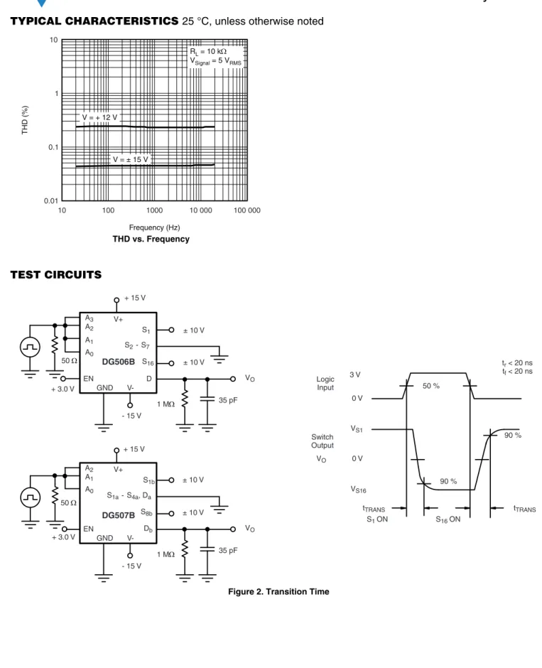
TEST CIRCUITS
THD vs. Frequency THD (%) Frequency (Hz) 0.01 10 100 1000 10 000 100 000 1 0.1 10 RL = 10 k VSignal = 5 VRMS V = ± 15 V V = + 12 VFigure 2. Transition Time A 1 A 0 A 2 A 1 A 0 + 15 V - 15 V EN V+ V- GND D 35 pF V O S1 S2 - S7 S16 1 M ± 10 V ± 10 V + 15 V - 15 V EN V+ V- GND 35 pF V O S1b S 1a - S 4a , D a S8b 1 M ± 10 V ± 10 V D b Logic Input Switch Output V S16 V O t TR A N S t r < 20 ns t f < 20 ns S16 ON S 1 ON t TR A N S 0 V V S1 50 % 90 % 90 % 3 V 0 V DG506B DG507B 50 + 3.0 V 50 + 3.0 V A3 A2
TEST CIRCUITS
Figure 3. Enable Switching Time Logic Input Switch Output V O t r < 20 ns t f < 20 ns 3 V 0 V 0 V tOFF(EN) tON(EN) 50 % 90 % 90 % VO EN S1 S2 - S16 A 0 A 1 A 2 50 Ω 1 kΩ V O V+ GND V- D 5 V 35 pF - 15 V + 15 V S 1b S 1a - S 8a, D a S 2b - S 8b D b EN A 0 A 1 50 Ω 1 kΩ V O V+ GND V- 5 V 35 pF - 15 V + 15 V DG506B DG507B A3 A2
Figure 4. Break-Before-Make Interval
50 % 80 % Logic Input Switch Output V O V O tOPEN t r < 20 ns t f < 20 ns 0 V 3 V 0 V EN V+ GND V- + 5 V 35 pF - 15 V + 15 V + 3.0 V A 2 D b , D All S and D a 1 k V O 50 A 1 A 0 DG506B DG507B A3
TEST CIRCUITS
Vishay Siliconix maintains worldwide manufacturing capability. Products may be manufactured at one of several qualified locations. Reliability data for Silicon Technology and Package Reliability represent a composite of all qualified locations. For related documents such as package/tape drawings, part marking, and reliability data, see www.vishay.com/ppg?65150.
Figure 5. Charge Injection A 0 EN A X V O V+ GND V- D - 15 V + 15 V R g S X C L 1 nF Channel Select 3 V 0 V OFF ON Logic Input Switch Output ΔVO
ΔVO is the measured voltage due to charge transfer error Q, when the channel turns of f .
QINJ = CL x ΔVO
OFF
Figure 6. Off Isolation
Figure 8. Insertion Loss
R L 50 Ω V OUT V+ GND V- - 15 V + 15 V A X D A 0 S 16 S 1 V S EN R g = 50 Ω Of f Isolation = 20 log V OU T V IN V IN 3 V R L 50 Ω A X V O D R g = 50 Ω
Insertion Loss = 20 log V OU T V IN A 0 V S S 1 V+ GND V- - 15 V + 15 V EN VIN 3 V Figure 7. Crosstalk
Figure 9. Source Drain Capacitance
RL 50 Ω V+ GND V-- 15 V + 15 V AX D A0 S16 SX VOUT EN Rg = 50 Ω
Crosstalk = 20 log VOUT VIN VIN S1 VS 3 V RL 50 Ω f = 1 MHz S 1 D EN + 15 V - 15 V GND V+ V- Meter Impedance Analyzer or Equivalent S 8 A 0 A X Channel Select 0 V or 3 V
TSSOP: 28ĆLEAD
4.400
NOTES:
1. Package Surface: Shiny Finish (Ro 0.15 – 0.20). 2. Package Warpage: 0.012 (max).
3. Package Corner Radius: R0.1 mm (max). 4. Top to BTM Cavity Mismatch: 0.037 (max). 5. Tolerance: "0.050 unless otherwise specified. 6. End Flash Max: 0.1016 mm.
Pin 1 Indicator O0.70x0.038"0.012 DP Surface Polished 0.735 " 0.025 6.400 " 0.050 1.016 " 0.025 0.686 " 0.050 0.432 " 0.020 0.457 " 0.020 0.127 T y p . 0.1 (Ref) 0.625 9.70"0.025 12_ (8X)
0.28 Typ. 0.65 Typ. Detail A
5.05"0.050 0.600"0.050 4_"2_ 5_–8_ Typ. R0.1–0.15 R0.1–0.15 1.00"0.050 Detail A All Corner R0.1 (max)
0.050
ECN: S-03946—Rev. C, 09-Jul-01 DWG: 5851
PLCC: 28-LEAD
D0.101 mm 0.004" D-SQUARE D1-SQUARE B B1 e1 A1 A A2 D2DIM. MILLIMETERS INCHES
MIN. MAX. MIN. MAX.
A 4.20 4.57 0.165 0.180 A1 2.29 3.04 0.090 0.120 A2 0.51 - 0.020 -B 0.331 0.553 0.013 0.021 B1 0.661 0.812 0.026 0.032 D 12.32 12.57 0.485 0.495 D1 11.430 11.582 0.450 0.456 D2 9.91 10.92 0.390 0.430 e1 1.27 BSC 0.050 BSC
ECN: T09-0766-Rev. D, 28-Sep-09 DWG: 5491
www.vishay.com
Vishay Siliconix
Revision: 01-Aug-11 1 Document Number: 71268
SOIC (WIDE-BODY): 28-LEADS
ECN: E11-2209-Rev. D, 01-Aug-11
DWG: 5850
0.3525 0.001 0.06 0.002D CAVITY NO. 0.295 0.001 0.070 0.005 0.1475 0.001 0.055 0.005 PIN 1 INDICATOR 0.047 0.007 0.001 dp SURFACE POLISHED 0.010 0.334 0.005 R0.004 R0.008 R0.009 R0.004 0.032 0.005 4° 2° 0.041 0.001 0.705 0.001 0.091 0.001 0.017 0.0003 0.050 TYP. 0.00825 ± 0.00325 0.098 0.002 0.334 0.005 0.291 0.001 0.295 0.001 0.406 0.004 R0.004 7°(4 ) 0.020 45° DETAIL A DETAIL A 1 2 3 4 5 6 7 8 28 27 26 25 24 23 22 21 9 10 20 19 11 18 12 17 13 16 14 15Revision: 02-Oct-12 1 Document Number: 91000