Correlation between damage evolution, structural and optical
properties of Xe implanted CrN thin films
Maja Popovi´c
1,∗, Mirjana Novakovi´c
1, Kun Zhang
2, Miodrag Mitri´c
1, Nataša Bibi´c
1,
Zlatko Rakoˇcevi´c
11University of Belgrade, Vinˇca Institute of Nuclear Sciences, 11321 Belgrade, Serbia
2Physikalisches Institut, Georg-August-Universität Göttingen, Friedrich-Hund-Platz 1, 37077 Göttingen,
Germany
Received 3 April 2018; Received in revised form 22 May 2018; Accepted 16 June 2018
Abstract
Polycrystalline CrN thin films were irradiated with Xe ions. The irradiation-induced modifications on struc-tural and optical properties of the films were investigated. The CrN films were deposited on Si(100) wafers with the thickness of 280 nm, by using DC reactive sputtering. After deposition, the films were implanted at room temperature with 400 keV Xe ions with the fluences of 5–20×1015ions/cm2. The films were then annealed at 700 °C in vacuum for 2 h. The combination of Rutherford backscattering spectrometry (RBS), X-ray diff rac-tion (XRD) and transmission electron microscopy (TEM) was used for structural analyses, while changes in optical properties were monitored by spectroscopic ellipsometry. We also measured the electrical resistivity of the samples using a four point probe method. RBS analysis reveals that the concentration of Xe in the lay-ers increases with ion fluence reaching the value of around 1.5 at.% for the highest ion dose, at a depth of 73 nm. XRD patterns show that the irradiation results in the decrease of the lattice constant in the range of 0.4160–0.4124 nm. Irradiation also results in the splitting of 200 line indicating the tetragonal distortion of CrN lattice. TEM studies demonstrate that after irradiation the columnar microstructure is partially destroyed within∼90 nm, introducing a large amount of damage in the CrN layers. Spectroscopic ellipsometry analysis
shows that the optical band gap of CrN progressively reduces from 3.47 eV to 2.51 eV with the rise in ion flu-ence up to 20×1015ions/cm2. Four point probe measurements of the films indicated that as the Xe ion fluence
increases, the electrical resistivity rises from 770 to 1607µΩcm. After post-implantation annealing crystalline grains become larger and lattice distortion disappears, which influences optical band gap values and electrical resistivity of CrN.
Keywords: CrN, thin films, XRD, ellipsometry, optical band gap
I. Introduction
Due to their excellent mechanical properties, transi-tion metal nitrides are widely used as protective coat-ings in industrial applications. Among them chromium nitride (CrN) has attractive combination of desirable physical, chemical and mechanical characteristics [1]. These remarkable characteristics such as high hard-ness (22–25 GPa), high wear- and corrosion resistance, low friction coefficient make it attractive for cutting tools and wear application, as diffusion barriers in the field of nano-electronics, and as corrosion and abrasion-∗
Corresponding authors: tel/fax:+381 11 6308 425, e-mail:[email protected]
resistant coatings on optical and mechanical compo-nents [2–4]. On the other hand, the CrN is also inter-esting due to its magnetic, optical and electronic prop-erties, after being reported as a semiconductor material in the recent studies [5].
To improve physical, chemical and mechanical prop-erties of thin films, the different treatments can be used such as doping, annealing, ion implantation, plasma treatment, etc. [6–11]. Among them ion implantation as a non-thermal and non-equilibrium technique possesses a series of advantages including accurate control of the ion concentration-depth distribution, incorporation of almost all elements in different systems conducted at room temperature thus offering interesting possibilities.
In addition, implanted xenon ions are known to form ag-gregates and bubbles in various materials such as Si3N4 [14], silicon [15], ZrC [16], graphite [17], aluminium [18], inducing swelling and cracks due to its low solubil-ity. It was found that due to xenon’s chemical inertness and relatively large atomic number the reaction process in the material can be simply described by as formation of the physical damage. Thus, a successful application of Xe ion implantation depends on understanding the production of damage in the film.
The goal of this study was to determine changes of the structural and optical properties of CrN thin films af-ter 400 keV Xe ions implantation. These changes were investigated on the basis of irradiation damage forma-tion and performed post-implantaforma-tion annealing. Opti-cal properties in conjunction with the structural param-eters, such as lattice constant and crystallite size are dis-cussed. An attempt was made to clarify whether the op-tical properties of the CrN layers could be controlled by combining ion irradiation and thermal annealing. It was shown that observed changes in optical band gap of CrN films can be directly correlated with the variation in crystallite size and damage induced by the irradiation of the films. The structural changes are also correlated to the measured electrical resistivity.
II. Experimental
2.1. Sample preparation
Polycrystalline CrN films with thickness of 280 nm were deposited by DC reactive sputtering in a commer-cial Bulzers Sputtron II system, using 1.5 keV argon ions and 99.9% pure Cr target. The chamber was evac-uated to 1×10⁻⁴Pa, while the argon and nitrogen
par-tial pressures were 1×10⁻¹Pa and 5×10⁻²Pa,
respec-tively. The substrates used were 550µm thick Si(100) wafers, which were cleaned in diluted hydrofluoric acid and deionized water, and kept at 150 °C during depo-sition. Experimental parameters were chosen so that the deposition rate at the substrate was ∼11 nm/min.
The CrN thin films were subsequently implanted with singly charged Xe ions with an ion energy of 400 keV by means of the Göttingen IONAS implanter [19]. The irradiations were performed at room temperature with
nace was kept around 10−6Pa during annealing. 2.2. Characterization techniques
The structural and optical characterizations of CrN thin samples irradiated with 400 keV Xe ions and an-nealed at 700 °C were done by Rutherford backscat-tering spectrometry (RBS), X-ray diffraction (XRD), transmission electron microscopy (TEM) and spectro-scopic ellipsometry. For studying the electrical proper-ties of the films four probe method was used.
Depth profiling of CrN films was performed by 900 keV He++ ion beam provided by the Göttingen IONAS implanter [19]. RBS spectra were taken with two silicon surface barrier detectors mounted at±165° with respect to the beam, having an energy resolution of 13 keV FWHM. The software used in simulation of RBS spectra was WiNDF code [21].
The XRD patterns of the samples were recorded us-ing PHILIPS PW1050 diffractometer with monochro-matized CuKα radiation (λ = 0.15418 nm) in Bragg-Brentano geometry. The XRD spectra were collected in a 2θscan range of 35–47° with a step size of 0.01° and an integration time of 0.5 s. Phase identification of the films was confirmed by matching the diffraction peaks with those of JCPDS database.
The characterization of the CrN films by transmis-sion electron microscopy in cross-section, was carried out by using PHILIPS CM30 microscope, operated at 300 keV voltage. The samples for TEM examination were prepared by conventional procedure including cut-ting and mouncut-ting of the samples onto copper slot, fol-lowed by polishing and Ar ions milling. In addition, micro-diffraction (MD) technique was used for study-ing the crystalline structure of the films.
The optical properties were characterized by using HORIBA-Jobin Yvon UVIS ellipsometer over the spec-tral range from 260 to 2066 nm. The spectra were recorded digitally using Delta Psi2 software, with a 0.1 eV intervals and a collection time of 200 ms per each point. The measurements were taken using 1 mm spot size under an incident angle of 70° with respect to the surface normal.
Sheet resistance of the samples was measured with a JANDEL RM 3000 Universal probe. The values were
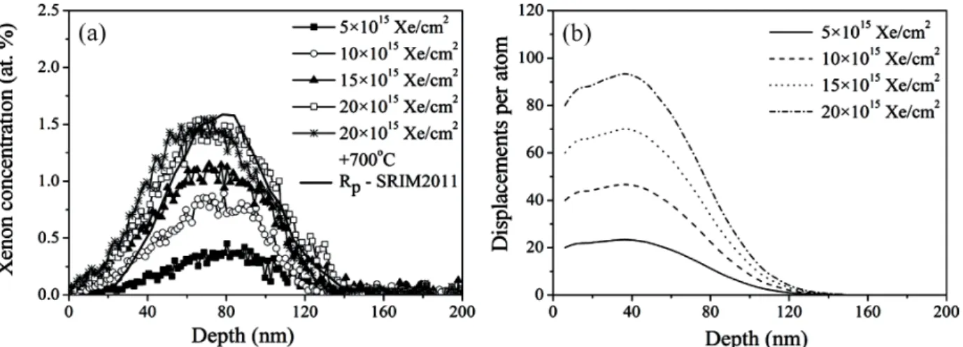
Figure 1. (a) Xe concentration depth profiles of CrN samples irradiated with different doses deduced by means of WiNDF code from the RBS spectra together with SRIM2011 calculation. The sample irradiated with 20×1015ions/cm2was measured and
analysed again after annealing for 2 h at 700 °C. (b) SRIM simulation of DPA value of 400 keV Xe ions irradiation on CrN films
calculated as specific resistivity to compare the results. III. Results and discussion
3.1. Xe distribution in CrN films
Compositional analysis done by RBS has shown that the as deposited CrN films obtained under the given de-position conditions have stoichiometry close to Cr : N = 1 : 1 [22]. The concentration profiles of implanted Xe calculated from the experimental RBS spectra using the ion beam analysis computer code WiNDF are pre-sented in Fig. 1a. The calculated spectra show that the maximum depth of xenon is up to 140 nm beneath the surface. As expected, the linear increase in the concen-tration of Xe ions with the rise in the ion fluence is ob-served. A maximum Xe concentration of about 1.5 at.% can be found in a depth of approximately 73 nm for the highest ion fluence. Also, with increasing ion fluence the position of the maximum was slightly shifted to-wards the surface which can be easily attributed to the concurrent sputtering which took place during ion irra-diation. These experimentally obtained depth distribu-tions are in agreement with the theoretically evaluated projected ion range ofRp ±∆Rp = 75±24 nm
calcu-lated by SRIM2011 program [20]. The Xe profile ex-tracted from the spectrum taken from the sample im-planted with the highest ion fluence and annealed 2 h at 700 °C is also included in Fig. 1a. As it can be observed, annealing of the sample further shifts the Xe profile to the surface. In particular, the maximum Xe concentra-tion is slightly lower as compared to the as-implanted sample, which is most probably result of Xe atom diff u-sion out of the sample due to the high-temperature an-nealing. Similar behaviour was already reported in the previous study for argon implanted CrN layers annealed at 700 °C [11].
The SRIM simulated damage events of CrN films in-troduced by Xe ions irradiation are illustrated in Fig. 1b. As it is shown, the calculated DPA (displacements per atom) for the fluences of 5, 10, 15 and 20×1015ions/cm2
was yielded to be 23, 47, 70 and 94, respectively. The calculations were achieved with K-P quick calculation and the DPAs were obtained using thevacancy.txtfile. The simulation suggests that the Xe ions with their large atomic number can introduce a large damage inside 130 nm of the films with the maximum at around 35 nm. To our knowledge Xe behaviour in CrN is not exam-ined experimentally. But, a few studies have been car-ried out on other transition metal-nitrides, such as TiN, influenced by Xe ions irradiation [23–25]. The authors in these reports found that the Xe ions produce a great damage in this kind of systems. Moreover, our recent experiments on the CrN system give evidence that the damage was produced along the ion track even after im-plantation with much lighter inert Ar ions [11,22].
3.2. XRD analysis of CrN films
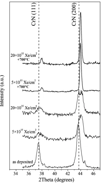
Our previous study [22] showed that the as-deposited CrN thin film has a polycrystalline structure with the crystallites aligned preferentially along (200) plane. XRD patterns of the as deposited CrN film and films ir-radiated with xenon ions at fluences of 5×10¹⁵ions/cm2
and 20×1015ions/cm2are shown in Fig. 2. Also, in Fig.
2 the patterns taken on the samples implanted with the fluence of 5×10¹⁵ions/cm2and 20×1015ions/cm2,
an-nealed 2 h at 700 °C are plotted. The presented spectral range was restricted to the region of 2θ=35–47°, where the changes were observed most clearly. Two peaks at 37.44° and 43.67° corresponding to the 111 and 200 lines of CrN cubic structure (Fm3m) are detected in the as deposited film, giving a lattice parameter a = 0.4160 nm. This value is very close to the value given by the JCPDS No. 00-011-0065 [26]. After implanta-tion with the fluence of 5×10¹⁵ions/cm2, the
crystallo-graphic cubic structure is preserved; the primary phase of the Xe-ion implanted films includes CrN 111 and CrN 200 lines, which are nearly identical to that of un-implanted CrN. It was found that after implantation the diffraction peaks shift to higher 2θ angles. Calculated from XRD data, the lattice constant of the Xe-ion
im-Figure 2. XRD diffraction patterns of prepared CrN samples (dashed lines correspond to the reference
values of CrN [26])
planted CrN film is a = 0.4133 nm, which is smaller than that of the as-deposited, hence resulting in approx-imately 1% of the lattice contraction. With further in-crease of ion fluence the peaks continue to shift, giving a slight decrease of lattice parameter to 0.4124 nm. The shifting nature of diffraction peaks in polycrystalline films after irradiation is believed to be associated with the build up of stress in CrN and change of its inter-planar spacing, which arise from the creation of high amount of defects in the films.
not react with any elements in CrN, but produce crystal defects with high rate resulting in the damaged struc-ture along the ion track. These defects generate addi-tional stress in the lattice, thus provoking a change in the lattice parameters for the irradiated samples. As in-dicated by the SRIM simulation, the as-produced DPA yields the value up to 94, which thus will impact the structure of the films. Note also the observed broaden-ing of 111 and 200 diffraction peaks in CrN after Xe ions irradiation, which is probably due to the damage induced microstrain in the cell, already reported in lit-erature [22,28]. The broadening of XRD lines is an in-dication of the formation of smaller grains. Indeed, the crystallite size was calculated [27], and it was found that the xenon ions led to the formation of slightly smaller grains.
In the patterns taken on the 5×10¹⁵ions/cm2 and
20×1015ions/cm2post-annealed samples (Figs. 2), the
peaks 111 and 200, belonging to CrN, are also clearly identified without trace of any other phases. It can be seen that after annealing there is no distortion of 200 line, the peak is narrow and much more intense as com-pared to as-implanted samples. It is implied that the peak narrowing behaviour could possibly originate from the grain growth and the annihilation of defects during annealing at high temperature. The estimated crystallite size increases after annealing to around 30 nm. The val-ues of peaks position, lattice constant, interplanar spac-ing and mean grain size calculated from the different spectra are summarized in Table 1.
3.3. TEM observations on CrN films
In previous experiments [22], the investigated CrN layers were found to grow in the form of columnar struc-ture, typical for sputter deposited metal-nitrides [29,30].
Table 1. XRD analysis of the as-deposited and ion-implanted CrN samples (diffaction angle 2θ, interplanar spacingd, lattice constantaand mean grain sizeD)
Sample (111) (200) d[nm] a[nm] D[nm] 2θ 2θ1/2θ2 As-deposited 37.4368 43.6732 0.2402 0.4160 14.5 5×10¹⁵Xe/cm2 37.6546 43.7225/44.1446 0.2389 0.4133 14.1 20×1015Xe/cm2 37.7059 43.6786/44.1856 0.2386 0.4124 14.0 5×10¹⁵Xe/cm2+700 °C 37.9847 43.9802 0.2387 0.4103 26.5 20×1015Xe/cm2+700 °C 37.9558 43.9915 0.2370 0.4100 30.6
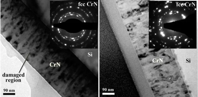
Figure 3. Bright-field cross-sectional TEM image of CrN film implanted with the fluence of 20×1015Xe/cm2before (a) and
after annealing at 700 °C (b) and corresponding MD diffraction patterns
In Figs. 3a and 3b bright field cross-sectional TEM im-ages of CrN sample implanted with the highest ion flu-ence of 20×1015ions/cm2 before and after annealing
in vacuum 2 h at 700 °C were presented. The corre-sponding MD patterns were taken in the same cross-sectional view, covering a layer, without underlying Si substrate and shown in the upper right part of the cor-responding image. In as-implanted sample (Fig. 3a) the destroyed columnar structure is clearly observed. Simi-lar behaviour was observed with the CrN samples im-planted with chromium ions, which was also investi-gated via TEM [31]. These structural changes appear to be the most pronounced within 90 nm of the layer, where the highest amount of energy is deposited in the collision processes, while the part of the layer towards the substrate remains practically unaffected. Diff rac-tion rings in the MD pattern identify isolated fcc CrN phase with very fine nanocrystalline grains indicating that the polycrystalline structure is retained after irradi-ation. Subsequent vacuum annealing of this implanted sample (Fig. 3b) affects the structure of the layer. A closer analysis shows that individual crystal grains grow much larger upon heat treatment [11]. MD pattern in this case still corresponds tofccCrN phase. Isolated bright spots on diffraction rings become sharper and bigger in-dicating the formation of larger grains due to the grain coalescence effect developed after 700 °C. This is in agreement with XRD findings according to which the grains become as large as∼30 nm (see Table 1).
3.4. Optical characterization
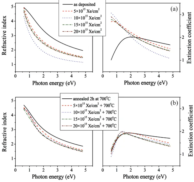
The influence of implanted Xe ions on the optical properties of CrN thin films is studied using spectro-scopic ellipsometry. Detailed information about optical parameters such as refractive indexn, and extinction co-efficientk, were obtained using an appropriate model in
fitting the experimental ψand∆ spectra. Good agree-ment obtained between measured and calculated ellip-sometric spectra indicates that the model used in the analysis is convenient and that the calculated results are reliable. The description of the model used in the fit-ting of experimental CrN spectra was described in detail in literature [11]. Figure 4 showsnandk spectra over the photon energy of 0.6–4.8 eV for CrN thin films im-planted with different Xe ion fluences and subsequently annealed at 700 °C, respectively. The spectrum of the as deposited film is also given for comparison with the spectra of the implanted films. We can notice that the as deposited film exhibits maximum values of refractive index in the low energy part of the spectrum and almost exponential decrease with increasing photon energy up to ultraviolet region (Fig. 4a). The optical constantnof our CrN layer quite well match with the one reported by Aouadiet al.[32]. After Xe ion implantation the inten-sity of the refractive index is changed while the slope of the curves remains the same. Thenvalues decrease with Xe ions and the change is most visible for the fluence of 10×1015ions/cm2. The refractive index dependence, in
turn, is a consequence of changes in the structure that increase with the number of implanted ions. The more implanted ions there are, the more defects exist, which lowers the refractive index. During the Xe ion implan-tation complex interactions between high energy parti-cles and target atoms occur, which lead to deformation of the lattice in the films as previously shown in XRD analysis. As for the extinction coefficient it was found thatkvalues for the as deposited sample increases with photon energy up to 2.0 eV, while decreases for higher energy values [32]. After Xe ions irradiation the shape of the extinction coefficient curves was changed. It can be seen that thek parameter is much more sensitive to the variation of irradiation fluence at lower photon
en-Figure 4. Refractive indexnand extinction coefficientk-spectra as a function of photon energy for Xe ion implanted CrN films (a) and subsequently annealed at 700 °C (b)
ergies, exhibiting notably higher values as compared to the as deposited sample. On the other hand, subsequent annealing of implanted samples did not significantly change the optical constants (Fig. 4b). The refractive in-dex and extinction coefficient curves show very similar shape as in the case of the as deposited sample, with slightly smaller absolute values, indicating that the de-fect concentration as well as crystallographic structure did not notably changed after the post-irradiation heat treatment.
From the extinction coefficient spectra the energy profiles of the absorption coefficient,α, have been de-rived (α = 4πk/λ) and shown in Fig. 5 for the Xe im-planted CrN films and subsequently annealed at 700 °C. The spectrum of the as deposited sample (Fig. 5a) shows the usual minimum absorption in the low energy re-gion and exponential increase with increasing photon energy. The presence of Xe ions changes the slope of absorption curves: as compared to the as deposited
sam-ple, higher absorption in the low energy region was ob-served, while Xe ions induce a decrease of absorption coefficient above the photon energy of 2.5 eV. These changes could be attributed to the production of defect levels in the band gap and/or to the increase of the car-rier concentration during irradiation or production of metallic Cr clusters due to the loss of nitrogen atoms. Similar effects were already observed for CrN films im-planted with Ar ions [11]. After annealing at 700 °C (Fig. 5b) the absorption coefficient did not change for the photon energies lower than 2 eV, and beyond this energy value it starts to decrease.
Significant parameter that characterizes semiconduc-tor and dielectric materials is the optical band gap en-ergy (Eg) which presents very important property in the
design and modelling of optical devices. The band gap energies of Xe implanted and also post-annealed CrN films are calculated using the following Tauc relation-ship [33]:
Figure 5. Absorption coefficients of CrN thin films irradiated with different Xe ion fluences (a) and post-annealed at 700 °C (b)
Table 2. Band gap values (Eg) of as-deposited, Xe ion irradiated and annealed CrN layers
Band gap energy,Eg[eV]
Dose/Treatment 0 5×10¹⁵ions/cm2 10×1015ions/cm2 15×1015ions/cm2 20×1015ions/cm2
Xe irradiated 3.47 3.05 2.92 2.77 2.51
Xe irradiated+700 °C 3.09 3.08 3.05 3.02 3.00
α·h·ν=A(h·ν−Eg)1/2 (1)
where Ais a constant, ν is the frequency of the inci-dent light andhis the Plank constant. Since Eg = hν
when (αhν)2 = 0, an extrapolation of the linear region of the plot of (αhν)2 versus photon energy (hν) on the
x-axis gives the value of the optical band gap. Figure 6 shows the Tauc plots for the Xe irradiated and post-annealed CrN thin films. The variation of band gap en-ergy with Xe ion fluence before and after annealing is presented in Fig. 7. The as deposited CrN film is found to have band gap energy of 3.47 eV which is slightly higher than the value of 3.4 eV reported by Fu et al.
[34]. After Xe ions irradiation, this value decreases and shows a progressive reduction with increasing the irradi-ation fluence. The observed red shift could be explained on the basis of increasing the degree of disorder and
density of defects due to the addition of Xe ions into CrN films. Consequently, energy band gap data show that CrN film has the lowest value of 2.51 eV after im-plantation with the fluence of 20×1015ions/cm2. It is
be-lieved that with the gradual increase of ion fluence the degree of implantation induced damage in the films is increased together with the monotonic decrease in their crystallinity. Hence, optical band gap decreases continu-ously with the increase of ion fluence. Similar behaviour was already observed in our previous report on 200 keV Ar ions implantation in CrN films [11]. Annealing at 700 °C does not have much effect on the band gap. A slightly decreasing trend was noticed.The band gap en-ergy varies with increasing ion fluence in the very nar-row range from 3.09 to 3.00 eV. The band gap values for all samples are summarized in Table 2. The band gap analyses of CrN films are overall well-consistent with XRD and TEM results.
Figure 7. Dependence of optical band gap energyEgof CrN films on the Xe ion fluence before and
after annealing at 700 °C
Figure 8. Electrical resistivity of CrN films irradiated with 400 keV xenon ions
3.5. Electrical resistivity measurements
In Fig. 8 the electrical resistivity of CrN samples implanted with Xe ions and annealed at 700 °C as a function of the irradiation fluence is plotted. The as deposited CrN film has a high resistivity of about 770µΩcm, which is 15% larger than the CrN bulk value. Such observations are in a good agreement with the work reported on CrN thin films fabricated by DC mag-netron sputtering [35]. Upon Xe ion irradiation with 5×10¹⁵ions/cm2the resistivity of CrN sample increases
by a factor of 2, and continues to increase with an ion dose. Obviously, ion induced damage in the layer has a predominant role on metallic behaviour of CrN lead-ing to an overall increase of electrical resistivity of CrN. These changes are much more pronounced in compari-son with Ar implanted CrN films [36] due to higher en-ergy of Xe ions and their larger atomic number which introduced considerable amounts of defects in the films. Having this in mind the resistivity of CrN can be easily changed in the wide range by varying Xe concentration in the layers. After annealing at 700 °C resistivity sig-nificantly decreased which can be attributed to the lower
nal distortion of CrN lattice. The observed variation in structure can be attributed to the formation of the high density damage region in the CrN structure. TEM anal-ysis found that this damage region is mainly distributed within∼90 nm from the surface of the CrN layer.
Fur-ther, the optical property measurement implies that the optical band gap for the Xe irradiated samples decreases gradually with increasing ion fluence. It is a combined result of the decrease of crystallite size and damage in-duced by the irradiation. The optical band gap for post-annealed samples remains nearly constant with increas-ing ion fluence. This could be mainly attributed to the formation of bigger crystallites and reduction of defects at higher temperature. The observed changes are corre-lated with the variation of electrical resistivity of the lay-ers. The changes of the structural and optical parameters with the increase of Xe irradiation fluence and after an-nealing at 700 °C have shown that the optical properties of CrN films are directly defined by the lattice disorder and hence can be tailored and controlled by combining ion irradiation and thermal annealing. The conclusions drawn in the present work suggest in which direction these studies could be possibly extended, namely a more systematic variation of ion fluences and annealing tem-perature over larger ranges.
Acknowledgement: This work was supported by the Ministry of Education and Science of the Republic of Serbia (Project No. III 45005). We would like to thank D. Purschke and P. Wilbrandt for their support during the experiments.
References
1. R.F. Bunshah, Handbook of Hard Coatings: Deposition
Technologies, Properties and Applications, Noyes
Publi-cation, Norwich, NY, 2001.
2. J. Lin, Z.L. Wu, X.H. Zhang, B. Mishra, J.J. Moore, W.D. Sproul, “A comparative study of CrNx coatings synthe-sized by dc and pulsed dc magnetron sputtering”, Thin
Solid Films,517(2009) 1887–1894.
3. S.H. Shin, M.W. Kim, M.C. Kang, K.H. Kim, D.H. Kwon, J.S. Kim, “Cutting performance of CrN and Cr-Si-N coated end-mill deposited by hybrid coating system for ultra-high speed micro machining”, Surf. Coat. Technol., 202(2008) 5613–5616.
4. S.-H. Lee, T.-H. Yang, S.-H. Hyun, Y.-S. Yoon, “Corrosion behavior of pre-oxidized and thermally nitrided stainless steel for polymer electrolyte membrane fuel cell bipolar plates”,Corros. Sci.,58(2012) 79–85
5. D. Gall, C.S. Shin, R.T. Spila, M. Odén, M.J.H. Senna, J.E. Greene, I. Petrov, “Growth of single-crystal CrN on MgO(001): Effects of low-energy ion-irradiation on sur-face morphological evolution and physical properties”,J.
Appl. Phys.,91(2002) 3589–3597.
6. Y.-Y. Chang, D.-Y. Wang, W. Wu, “Tribological enhance-ment of CrN coatings by niobium and carbon ion implan-tation”,Surf. Coat. Technol.,177-178(2004) 441–446. 7. K. Ibrahim, M. Mahbubur Rahman, X. Zhao, J.-P. Veder,
Z.-F. Zhou, E. Mohammadpour, R.H. Majeed, A.N. Nikoloski, Z.-T. Jiang, “Annealing effects on microstruc-tural, optical, and mechanical properties of sputtered CrN thin film coatings: Experimental studies and finite element modeling”,J. Alloys Compd.,750(2018) 451–464. 8. M. Mahbubur Rahman, Z.-T. Jiang, Z. Xie, X. Duan, Z.-f.
Zhou, P.C. Wo, C.-Y. Yin, N. Mondinos, Q. Gu, H. Wid-jaja, K. Jack, A. Yago, A. Amri, “Understanding local bonding structures of Ni-doped chromium nitride coatings through synchrotron radiation NEXAFS spectroscopy”,J.
Phys. Chem. C,118(2014) 18573–18579.
9. K. Ibrahim, M. Mahbubur Rahman, H. Taha, E. Moham-madpour, Z. Zhou, C.-Y. Yin, A. Nikoloski, Z.-T. Jiang, “Structural, morphological, and optical characterizations of Mo, CrN and Mo:CrN sputtered coatings for potential solar selective applications”,Appl. Surf. Sci.,440(2018) 1001–1010.
10. M. Mahbubur Rahman, Z.-T. Jiang, X. Duan, Z. Xie, A. Tadich, Z.-f. Zhou, N. Mondinos, C.-Y. Yin, M. Al-tarawneh, B.Z. Dlugogorski, “NEXAFS N K-edge study of the bonding structure on Al/Si doped sputtered CrN coatings”,J. Alloys Compd.,661(2016) 268–273. 11. M. Novakovi´c, M. Popovi´c, K. Zhang, Z. Rakoˇcevi´c, N.
Bibi´c, “Effects of 200 keV Ar-ions irradiation on the struc-tural and optical properties of reactively sputtered CrN films”,Opt. Mater.,62(2016) 57–63.
12. M. Novakovi´c, M. Popovi´c, E. Schmidt, P. Schöppe, M. Mitri´c, N. Bibi´c, C. Ronning, Z. Rakoˇcevi´c, “Evolution of structural and optical properties of Ag implanted CrN thin films with annealing temperature”,J. Alloys Compd.,729 (2017) 671–678.
13. M. Novakovi´c, M. Popovi´c, E. Schmidt, M. Mitri´c, N. Bibi´c, Z. Rakoˇcevi´c, C. Ronning, “Clustering of gold par-ticles in Au implanted CrN thin films: The effect on the SPR peak position”,Appl. Surf. Sci.,426(2017) 667–673. 14. Y.-U. Heo, M. Takeguchi, K. Mitsuishi, M. Song, Y. Nakayama, K. Furuya, “Precipitation behavior of Xe at grain boundaries in Si3N4ceramic during implantation at elevated temperature”, J. Nucl. Mater.,397 (2010) 122– 127.
15. G. Faraci, A.R. Pennisi, F. Zontone, “Fine structure effects and phase transition of Xe nanocrystals in Si”,Eur. Phys. J. B,51(2006) 209–213.
16. G. Gutierrez, N. Toulhoat, N. Moncoffre, Y. Pipon, A. Maître, M. Gendre, A. Perrat-Mabilon, “Thermal behavior of xenon in zirconium carbide at high temperature: Role of residual zirconia and free carbon”,J. Nucl. Mater.,416 (2011) 94–98.
17. R.G. Lacerda, M.C. Dos Santos, L.R. Tessler, P. Ham-mer, F. Alvarez, F.C. Marques, “Pressure-induced physical
changes of noble gases implanted in highly stressed amor-phous carbon films”,Phys. Rev. B: Condens. Matter,68 (2003) 054104.
18. R.S. Dhaka, C. Biswas, A.K. Shukla, S.R. Barman, “Xe and Ar nanobubbles in Al studied by photoemission spec-troscopy”, Phys. Rev. B: Condens. Matter, 77 (2008) 104119.
19. M. Uhrmacher, K. Pampus, F.J. Bergmeister, D. Purschke, K.P. Lieb, “Energy calibration of the 500 kV heavy ion im-planter ionas”,Nucl. Instrum. Meth. B,9(1985) 234–242. 20. J.F. Ziegler, J.P. Biersack, U. Littmark,The Stopping and
Range of Ions in Solids, Pergamon Press, New York, 1985.
21. N.P. Barradas, C. Jeynes, R.P. Webb, “Simulated annealing analysis of Rutherford backscattering data”, Appl. Phys.
Lett.,71(1997) 291–293.
22. M. Novakovi´c, M. Popovi´c, N. Bibi´c, “Ion-beam irradia-tion effects on reactively sputtered CrN thin films”,Nucl.
Instrum. Meth. B,268(2010) 2883–2887.
23. M. Popovi´c, M. Novakovi´c, M. Mitri´c, K. Zhang, Z. Rakoˇcevi´c, N. Bibi´c, “Xenon implantation effects on the structural and optical properties of reactively sputtered ti-tanium nitride thin films”,Mater. Res. Bull.,91(2017) 36– 41.
24. S. Gavarini, N. Toulhoat, C. Peaucelle, P. Martin, J. Mende, Y. Pipon, H. Jaffrezic, “Xenon migration be-haviour in titanium nitride”,J. Nucl. Mater.,362 (2007) 364–373.
25. R. Bès, C. Gaillard, N. Millard-Pinard, S. Gavarini, P. Martin, S. Cardinal, C. Esnouf, A. Malchère, A. Perrat-Mabilon, “Xenon behavior in TiN: A coupled XAS/TEM study”,J. Nucl. Mater.,434(2013) 56–64.
26. Z.G. Pinsker, L.N. Abrosimova,Kristallografiya,3(1958) 281.
27. R.W. Cheary, A. Coelho, “A fundamental parameters ap-proach to X-ray line-profile fitting”,J. Appl. Crystallogr., 25(1992) 109–121.
28. M. Novakovi´c, M. Popovi´c, N. Bibi´c, “Ion-beam irradia-tion effects on reactively sputtered CrN layers”,Process.
Appl. Ceram.,5[1] (2011) 25–29.
29. A.P. Ehiasariana, W.-D. Münz, L. Hultman, U. Helmers-son, I. Petrov, “High power pulsed magnetron sputtered CrNx films”,Surf. Coat. Technol.,163(164) (2003) 267– 272.
30. M. Popovi´c, M. Novakovi´c, N. Bibi´c, “Annealing effects on the properties of TiN thin films”,Process. Appl. Ce-ram.,9[2] (2015) 67–71.
31. S. Han, H.-Y. Chen, K-L. Chang, K.-W. Weng, D.-Y. Wang, F.-H. Lub, H.C. Shih, “Effects of MEVVA-implanted chromium on the structure and properties of CrN film”,Thin Solid Films,447-448(2004) 425–429. 32. S.M. Aouadi, D.M. Mihut, M.L. Kuruppu, S.R.
Kirk-patrick, S.L. Rohde, “Spectroscopic ellipsometry measure-ments of chromium nitride coatings”,J. Vac. Sci. Technol. A,19(2001) 2800–2804.
33. J.C. Tauc, Optical Properties of Solids, North-Holland, Amsterdam, 1972.
34. Y. Fu, M. Hou, G. Lin, J. Hou, Z. Shao, B. Yi, “Coated 316L stainless steel with CrxN film as bipolar plate for PEMFC prepared by pulsed bias arc ion plating”,J. Power
Sources,176(2008) 282–286.
35. B. Subramanian, K. Prabakaran, M. Jayachandran, “In-fluence of nitrogen flow rates on materials properties of CrNxfilms grown by reactive magnetron sputtering”,Bull.