User’s Guide
Introduction
Thank you for choosing the Lattice Semiconductor MachXO2™ Pico Development Kit.
This guide describes how to begin using the MachXO2 Pico Development Kit, an easy-to-use platform for rapidly prototyping system control designs using MachXO2 PLDs. Along with the evaluation board and accessories, this kit includes the pre-loaded Pico SoC Demo (Environment Scanning Demonstration Design) that demonstrates board diagnostic functions including ultra-low power, LCD driver, I/O control, current measuring, time stamps and data logging to non-volatile memory using the 8-bit LatticeMico8™ microcontroller.
The contents of this user’s guide include demo operation, top-level functional descriptions of the various portions of the evaluation board, descriptions of the on-board connectors, switches, a complete set of schematics and the bill of materials for the MachXO2 Pico Evaluation Board.
Note: Static electricity can severely shorten the lifespan of electronic components. See the MachXO2 Pico Devel-opment Kit QuickSTART Guide for handling and storage tips.
Features
The MachXO2 Pico Development Kit includes:
• MachXO2 Pico Evaluation Board – The MachXO2 Pico Evaluation Board features the following on-board com-ponents and circuits:
– MachXO2 LCMXO2-1200ZE PLD device in a 132-ball csBGA package. The board is designed for density migration, allowing a lower density MachXO2 device to be assembled on the board.
- Part number P-EVN is populated with the R1 silicon. Part number LCMXO2-1200ZE-P1-EVN is populated with the Standard silicon. The demos have been targeted for a specific version of silicon and are not interchangeable. For more information on the R1 to Standard migration refer to
AN8086, Designing for Migration from MachXO2-1200-R1 to Standard (Non-R1) Devices
- 4 Mbit SPI Flash memory
– Current sensor circuits using Delta-Sigma ADC – LCD driven with PWM analog output circuitry
– Expansion header for JTAG, SPI, I2
C and PLD I/Os – 4 capacitive touch sense buttons
– Standard USB cable for device programming – RS-232/USB and JTAG/USB interface – RoHS-compliant packaging and process – USB or 2032 battery powered
• Pre-loaded Reference Designs and Demo – The kit includes a pre-loaded Pico SoC Demo design that inte-grates several Lattice reference designs including: the LatticeMico8 microcontroller, master WISHBONE bus controller, soft delta-sigma ADC, SPI master controller, UART peripheral, Embeded Block RAM and additional control functions.
• USB connector Cable – A mini B USB port provides power, a communication and debug port via a USB-to-RS-232 physical channel and programming interface to the MachXO2 JTAG port.
• Battery – A 2032 coin battery can provides an alternate source of power.
• QuickSTART Guide – Provides information on connecting the MachXO2 Pico Evaluation Board, installing Win-dows hardware drivers, and running the Pico SoC Demo.
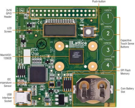
Figure 1. MachXO2 Pico Evaluation Board, Top Side USB Interface Socket 2x16 GPIO Header LCD Screen MachXO2-1200ZE I2C Temperature Sensor Coin Battery Slot SPI Flash Memory Capacitive Touch Sense Buttons Push-button
MachXO2 Device
This board features a MachXO2 PLD with a 1.2V core supply. The PLD is packaged in a 132-ball csBGA which pro-vides a migration path to devices ranging from 640 LUTs to 4340 LUTs. A complete description of this device can
be found in the MachXO2 Family Handbook.
Software Requirements
You should install the following software before you begin developing designs for the evaluation board: • Lattice Diamond™ 1.2 (or higher)
• ispVM™ System 17.9.1 (or higher)
Demonstration Design
Lattice provides the Pico SoC Demo design programmed in the board. The design utilizes the MachXO2 in the con-text of low power applications.
The Pico SoC Demo illustrates the use of the LatticeMico8 microcontroller, associated peripherals and firmware to provide a low power system featuring voltage/current measurement, data logging to nonvolatile memory, I/O con-trol, embedded block RAM utilization, UART communication, capacitive touch sense buttons and a LCD controller. • The LatticeMico8 executable program initializes the peripherals that are embedded in the SoC design. During
ini-tialization, the LatticeMico8 uploads the user menu on the Terminal of a PC.
• Users interact with LatticeMico8 and the board through the Terminal of a PC or through the capacitive touch sense buttons.
Figure 2. Pico SoC Demo Block Diagram
MachXO2 Pico Evaluation Board MachXO2-1200ZE
UART Capacitive Touch LCD Sense Buttons LatticeMico8 Microcontroller Master SPI Soft ADC Master I2C SPI Flash Analog Signal PC I2C Temp Sensor Embedded Block RAM
Power management is handled in two phases by the MachXO2 Pico Evaluation Board system:
1. MachXO2 Function – After the reset is de-asserted, LatticeMico8 initializes the peripherals embedded in the
MachXO2 device and uploads the user menu onto the HyperTerminal window of a PC.
Figure 3. HyperTerminal User Menu
2. Users interact with LatticeMico8 microcontroller and the board by selecting the available options in the HyperTerminal menu. The available options are:
• ‘s’ – This option reads the device ID of the SPI Flash on the board. The results are displayed to the terminal and the LCD.
• 't' - This option reads the I2C temperature sensor on the board. The result is displayed to the Terminal and to the
LCD. Button 4 on the board performs the same function but the result is only displayed on the LCD
• 'r' This option samples the capacitive touch buttons on the board and displays the data in the terminal.
• "0-9" - These values will echoed to the terminal and displayed on the LCD
• 'l' - This option will read the Icc, Icco, and Temperature and log it to the SPI flash memory. The WRITE page
pointer will increment when 'l' is pressed. The initial value of the page pointer after power up is a 0. Button 1 on the board performs the same function the LCD will display 8888
• 'd' - This option will read the data from the SPI Flash device and display to to the Terminal window. The READ
page pointer will increment when 'd' is pressed. The intial value of the page pointer after a power up is 0.
• 'c' - This option will clear (reset) the WRITE and READ page pointers
• 'e' - This selection will perform a bulk-erase of the Flash memory in the SPI Flash device and will clear (reset) the
WRITE and READ page pointers.
Setting up the Board
Drivers and Firmware
Before you begin, you will need to obtain the necessary hardware drivers for Windows from the Lattice web site.
1. Browse to www.latticesemi.com/alpha-mxo2-pico-kit and locate the hardware device drivers for the USB
inter-face.
2. Download the ZIP file to your system and unzip it to a location on your PC. Linux Support:
The USB interface drivers for the evaluation board are included in Linux kernel 2.4.20 or greater, including distribu-tions compatible with Lattice Diamond design software (Red Hat Enterprise v.3, v.4 or Novell SUSE Enterprise v.10).
The Pico SoC Demo is preprogrammed into the MachXO2 Pico Evaluation Board, however over time it is likely that your board will be modified.
To download the demo source files and reprogram the MachXO2 Pico Evaluation Board:
1. Download the demo appliction source code from www.latticesemi.com/alpha-mxo2-pico-kit.
2. Use .\Environment_Scanning_demo\project\impl1\Environment_Scanning_demo_impl1.jed to
restore the Environment Scanning demonstration design.
Connecting to the MachXO2 Pico Evaluation Board
1. Connect the evaluation board to your PC using the USB cable provided. The USB connector on the board
includes reference designator J1. Once the connection is made, a blue LED with reference designator D2 will illuminate.
2. If you are prompted “Windows may connect to Windows Update”, select No, not this time from available
options and click Next to proceed with the installation.
3. Choose the Install from specific location (Advanced) option and click Next.
4. Select Search for the best driver in these locations and click the Browse button to browse to the
Win-dows driver folder created earlier. Select the CDM 2.04.06 WHQL Certified folder and click OK.
5. Click Next. A screen will display as Windows copies the required driver files. Windows will display a
Programming the MachXO2
Using ispVM System software, users can scan and perform JTAG operations, including programming, with the MachXO2 device.
Setting Up Windows HyperTerminal
You will use a terminal program to communicate with the evaluation board. The following instructions describe the Windows HyperTerminal program which is found on most Windows PCs. You may use another terminal program but setup will be somewhat different. Windows 7 does not include HyperTerminal. Tera Term has been verified to work with Windows 7. For Linux, Minicom is a good alternative.
Note: This step uses the procedure for Windows XP users. Steps may vary slightly if using another Windows ver-sion.
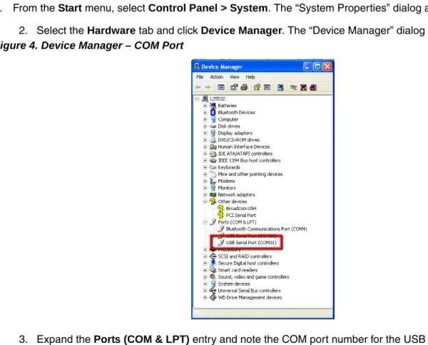
1. From the Start menu, select Control Panel > System. The “System Properties” dialog appears.
2. Select the Hardware tab and click Device Manager. The “Device Manager” dialog appears.
Figure 4. Device Manager – COM Port
3. Expand the Ports (COM & LPT) entry and note the COM port number for the USB Serial Port.
4. From the Start menu, select Programs > Accessories > Communications > HyperTerminal. The
Figure 5. New Connection – COM Port
5. Specify a Name and Icon for the new connection. Click OK. The “Connect To” dialog appears.
6. Select the COM port identified in Step 3 from the Connect using: list. Click OK.
Figure 6. Selecting the COM Port
7. The “COMn Properties” dialog appears where “n” is the COM port selected from the list.
8. Select the following Port Settings and click OK.
Bits per second: 115200
Data bits: 8
Parity: None
Stop bits: 1
Flow control: None
9. The HyperTerminal window appears.
10. From the MachXO2 Pico Evaluation Board, press the reset push-button with reference designator S1. The Pico SoC demo main menu appears.
Setting Up Linux Minicom
Minicom is a terminal program found with most Linux distributions. It can be used to communicate with the MachXO2 Pico Evaluation Board.
To setup Minicom:
1. Check active serial ports:
#dmesg | grep tty
Note the tty label assigned to the USB port 2. From a command prompt, start Minicom:
#minicom –s
The configuration menu appears.
3. Highlight Serial port setup and press Enter. Serial port settings appear.
4. Press A (Serial Device). Specify the active serial device noted in Step 1 and press Enter.
5. Press E (Bps/Par/Bits). Specify 115200, None, 8 and press Enter.
6. Press F (Hardware Flow Control). Specify None and press Enter.
7. Press Esc. The configuration menu appears.
8. Select Save setup as dfl. Minicom saves the port setup as the new default.
9. Select Exit. The Minicom interface appears.
10. From the evaluation board, press the S1 push-button (GSR). The Pico SoC demo main menu appears.
Ordering Information
Description Ordering Part Number
China RoHS Environment-Friendly Use Period (EFUP)
MachXO2 Pico Development Kit LCMXO2-1200ZE-P-EVN
Technical Support Assistance
Hotline: 1-800-LATTICE (North America)
+1-503-268-8001 (Outside North America)
e-mail: [email protected]
Revision History
Date Version Change Summary
February 2011 01.0 Initial release.
April 2011 01.1 Updated Pico Evaluation Board Top Side diagram, Pico SoC Demo
block diagram, HyperTerminal User Manual information, Appendix A and Appendix B.
June 2011 01.2 Added Appendix C.
July 2011 01.3 Updated Features list with information on migration from
MachXO2-1200-R1 to Standard (non-R1) devices.
July 2011 01.4 Added limitations section to Appendix C.
December 2011 01.5 Added Appendix D.
February 2012 01.6 Updated document with new corporate logo.
June 2012 01.7 Added Appendix D, Dual Boot Demonstration.
Updated Appendix E, Limitations.
June 2012 01.8 Added “MachXO2 Pico Evaluation Board I2C Bus Power Enable”
dia-gram to Appendix D.
July 2012 01.9 Appendix D figure title changed from “MachXO2 Pico Evaluation Board
I2C Bus Power Enable” to “MachXO2 Pico Evaluation Board SPI/I2C Bus
Power Enable”.
© 2012 Lattice Semiconductor Corp. All Lattice trademarks, registered trademarks, patents, and disclaimers are as
listed at www.latticesemi.com/legal. All other brand or product names are trademarks or registered trademarks of
Appendix A. Schematic
Figure 8. USB 5V, MachXO2 Power Rails, 3.0V Battery, 1.2V Rail and Current Monitors
4 4 3 3 2 2 1 1 D C B A +3. 3 V o rB at +1. 2 V +1. 2 V VCC_ CO RE +5V +3. 3 V +5V VCC_ IO VCCI O _ EXT +5V Da te : Si z e Sc h e m a ti c Re v of S h eet Ti tl e L a ttic e S e m ic o n d u c to r A p p lic a tio n s E m ai l: t e chsuppor t@ Lat ti ce se m i. c om P h one ( 5 03) 2688001 -o ( 8 00) LA TTI C E Bo a rd Re v Pr o je c t Fr iday, M ar c h 4, 2011 B 6 1 U S B 5 V , X O P o w e r R a ils 3 .0 V B a tt, 1 .2 V R a il and C ur re n t M o ni to rs M ACHXO 2 Pi c o Bo a rd E A Da te : Si z e Sc h e m a ti c Re v of S h eet Ti tl e L a ttic e S e m ic o n d u c to r A p p lic a tio n s E m ai l: t e chsuppor t@ Lat ti ce se m i. c om P h one ( 5 03) 2688001 -o ( 8 00) LA TTI C E Bo a rd Re v Pr o je c t Fr iday, M ar c h 4, 2011 B 6 1 U S B 5 V , X O P o w e r R a ils 3 .0 V B a tt, 1 .2 V R a il and C ur re n t M o ni to rs M ACHXO 2 Pi c o Bo a rd E A Da te : Si z e Sc h e m a ti c Re v of S h eet Ti tl e L a ttic e S e m ic o n d u c to r A p p lic a tio n s E m ai l: t e chsuppor t@ Lat ti ce se m i. c om P h one ( 5 03) 2688001 -o ( 8 00) LA TTI C E Bo a rd Re v Pr o je c t Fr iday, M ar c h 4, 2011 B 6 1 U S B 5 V , X O P o w e r R a ils 3 .0 V B a tt, 1 .2 V R a il and C ur re n t M o ni to rs M ACHXO 2 Pi c o Bo a rd E A Cor e Cur re nt I/O C u rre n t + 1 .2 V R a il CR2032 Ba tte ry C lip / Opt ional Char ger T o U 9 sen se f o r cur re nt T h in sig n al t races Direct p a th f ro m R34 to U 7 +5. 0 V_USB_CA BLE -> +3. 3 V Rai l +3. 3 V_USB T o U 9 sen se f o r cur rent T h in sig n al t races o r n o n lo ad bear ing c o ppe r pour Dir e c t pa th fr om R 3 5 to U 7 T P 1-T P 4 are 10mil f ree V ia' s L o cat e T P 1 & T P 2 v e ry close to R3 5 L o cat e T P 3 & T P 4 v e ry close to R3 4 U S B p lu g g ed in = > + 5 V is H igh, Q4 = O N , Q5 = O FF U S B un pl ugge d = > + 5 V i s Low , Q4 = O F F , Q 5 = O N R2 7 10k DI SM /R _0603 R2 7 10k DI SM /R _0603 R5 100k DI R5 100k DI TP4 DI TP4 DI 1 TP3 DI TP3 DI 1 C2 1 1uF DI C2 1 1uF DI Q4 LM L6402P bF DI Q4 LM L6402P bF DI R1 8 1 SM /R _0603 DI 1% R1 8 1 SM /R _0603 DI 1% Q2 IR F 2 4 0 Q2 IR F 2 4 0 + C76.8uF DI SM /C _1206 + C76.8uF DI SM /C _1206 R5 3 1M DNI R5 3 1M DNI D3 N S R 0530P 2T5G DNI D3 N S R 0530P 2T5G DNI D2 Blu e DI S M /D _0603 D2 Blu e DI S M /D _0603 C810uF DI SM /C _0805 C810uF DI SM /C _0805 C2 1uF DI C2 1uF DI 9 9 R6 0 1k DI S M /R _0603 R6 0 1k DI S M /R _0603 R5 4 4. 7k DI S M /R _0603 R5 4 4. 7k DI S M /R _0603 R2 8 100k DI S M /R _0603 R2 8 100k DI S M /R _0603 R1 9 1M DI S M /R _0603 R1 9 1M DI S M /R _0603 P 1703T-1202E /C B P 1703T-1202E /C B 2 BT1 B a tt_ C e ll_ H o ld e r BT1 B a tt_ C e ll_ H o ld e r Vb a t+ 3 Vb a t+2 2 V-1 R2 4 20 DNI SM /R _0603 R2 4 20 DNI SM /R _0603 R2 9 10k DI R2 9 10k DI R8 5 1 S M /R _0603 DI 1% R8 5 1 S M /R _0603 DI 1% U8 N C P 1117 DI S O T-223_che c kpi ns U8 N C P 1117 DI S O T-223_che c kpi ns GN D 1 IN 3 OU T 2 TA B 4 Q1 IRLM L6402P bF DI Q1 IRLM L6402P bF DI TP1 DI TP1 DI 1 TP2 DI TP2 DI 1 Q3 IR LM L6402P bF DI Q3 IR LM L6402P bF DI
Figure 9. Current Sense Amplifiers, Power Enable Mux 5 5 4 4 3 3 2 2 1 1 D D C C B B A A PW R_ AM P PW R_ AM P +3. 3 Vor B at Vr e fi n Vr e fi n +1. 2 V VCC_ CO RE VCCI O _ EXT VCC_ IO +3. 3 Vor B at +3. 3 Vor B at VCC_ IO PW R_ AM P Vre fi n PW R_ I2 CSPI En AM P [pg5] DSVr e fVc c [p g 5 ] D S O u tV c c [p g 5 ] DSI n Vc c [p g 5 ] DSVr e fVc c o [p g 5 ] D S O u tV cco [pg5] D S In V cco [p g5] En AM P [p g 5 ] En I2 CSPI [p g 5 ] Da te : Si z e Sc h e m a ti c Re v of S h eet Ti tl e L a ttic e S e m ic o n d u c to r A p p lic a tio n s E m a il : t ec h s u p p o rt @ L a tt ic es em i. c o m P hone ( 503) 2688001 -or - ( 800) LA TTI C E B oar d R e v Pr o je c t Fr iday, M ar c h 4, 2011 B A 6 2 Cu rr e n t Se n s e Am p li fi e rs , Po we r En a b le M u x M ACHXO 2 Pi c o Bo a rd E Da te : Si z e Sc h e m a ti c Re v of S h eet Ti tl e L a ttic e S e m ic o n d u c to r A p p lic a tio n s E m a il : t ec h s u p p o rt @ L a tt ic es em i. c o m P hone ( 503) 2688001 -or - ( 800) LA TTI C E B oar d R e v Pr o je c t Fr iday, M ar c h 4, 2011 B A 6 2 Cu rr e n t Se n s e Am p li fi e rs , Po we r En a b le M u x M ACHXO 2 Pi c o Bo a rd E Da te : Si z e Sc h e m a ti c Re v of S h eet Ti tl e L a ttic e S e m ic o n d u c to r A p p lic a tio n s E m a il : t ec h s u p p o rt @ L a tt ic es em i. c o m P hone ( 503) 2688001 -or - ( 800) LA TTI C E B oar d R e v Pr o je c t Fr iday, M ar c h 4, 2011 B A 6 2 Cu rr e n t Se n s e Am p li fi e rs , Po we r En a b le M u x M ACHXO 2 Pi c o Bo a rd E Del ta Si g I c co Measur ement Pow e r Suppl y Enabl e Mux Del ta Si g I c c Measur ement
High = Powered (S1)Low = Disabled (S2)
High = Powered (S1)Low = Disabled (S2)
R7 5 0 DI R7 5 0 DI R4 5 50 0.1% DI R4 5 50 0.1% DI C2 6 0. 1uF DI C2 6 0. 1uF DI R9 1 500 DI 1% R9 1 500 DI 1% R6 5 0 DI R6 5 0 DI R3 9 50 0.1% DI R3 9 50 0.1% DI R4 6 2k DI 1% R4 6 2k DI 1% C2 5 0. 1uF DI C2 5 0. 1uF DI C2 2 220pF DI C2 2 220pF DI R3 8 2k 0.1% DI R3 8 2k 0.1% DI -+ U1 5 B LM P 7708 DI B -+ U1 5 B LM P 7708 DI B 5 6 7 8 4 -+ U1 5 A LM P 7708 DI A -+ U1 5 A LM P 7708 DI A 3 2 1 8 4 R6 4 0 DI R6 4 0 DI C2 7 220pF DI C2 7 220pF DI R7 9 1k DI 1% R7 9 1k DI 1% R6 1 2k DI 1% R6 1 2k DI 1% R4 2 2k DI 0. 1% R4 2 2k DI 0. 1% U2 1 S T G 3 693Q TR U2 1 S T G 3 693Q TR 1S 2 1 123S E L 3 2S 1 4 D2 5 2S 2 6 GN D 11 3S 1 7 D3 8 3S 2 9 4S E L 10 4S 1 12 D4 13 4S 2 14 VCC 2 1S 1 15 D1 16 U2 0 S T G 3 693Q TR U2 0 S T G 3 693Q TR 1S 2 1 123S E L 3 2S 1 4 D2 5 2S 2 6 GN D 11 3S 1 7 D3 8 3S 2 9 4S E L 10 4S 1 12 D4 13 4S 2 14 VCC 2 1S 1 15 D1 16 C3 0 0. 047uF DI C3 0 0. 047uF DI R5 2 50 0.1% DI R5 2 50 0.1% DI R8 9 0 DI R8 9 0 DI R4 1 50 0.1% DI R4 1 50 0.1% DI C1 9 0. 047uF DI C1 9 0. 047uF DI R5 0 1k DI 1% R5 0 1k DI 1% R5 1 2k 0.1% DI R5 1 2k 0.1% DI C2 4 0. 1uF DI C2 4 0. 1uF DI R4 9 0 DI R4 9 0 DI R9 6 0 DI R9 6 0 DI R9 7 0 DI R9 7 0 DI R8 1 500 DI 1% R8 1 500 DI 1% R4 0 0 DI R4 0 0 DI R5 8 1k DI 1% R5 8 1k DI 1% R9 2 1k DI 1% R9 2 1k DI 1% R5 7 2k 0.1% DI R5 7 2k 0.1% DI
Figure 10. USB to JTAG and I2
C for the MachXO2
4 4 3 3 2 2 1 1 D C B A EESK EEDATA H LD _D e bug EECS S B +3. 3 V +3. 3 V or B at +3. 3 V VCC1 8 F T +3. 3 V +3. 3 V +3. 3 V PW R_ ENABL E b [p g 1 ] USB_ SCL [p g 4 ,5 ] USB_ TCK [p g 5 ] USB_ T D I [p g 5 ] USB_ T D O [p g 5 ] U S B _ TM S [pg5] USB_ SDA [p g 4 ,5 ] BDBUS1 [p g 5 ] BDBUS2 [p g 5 ] BDBUS0 [p g 5 ] BDBUS3 [p g 5 ] BDBUS4 [p g 5 ] BDBUS5 [p g 5 ] BDBUS6 [p g 5 ] BDBUS7 [p g 5 ] U S B _12M H Z [pg4] Da te : Si z e Sc h e m a ti c Re v of S h eet Ti tl e Lat ti c e S e m iconduct o r A p pl ic at io ns E m ai l: t e chsuppor t@ Lat ti c e s e m i. com P hone ( 5 03) 2688001 -or - ( 8 00) LA TTI C E B oar d R e v Pr o je c t Fr iday, M ar c h 4, 2011 B 6 3 U S B to J T A G a n d I2 C fo r th e X O 2 M ACHXO 2 Pi c o Bo a rd E A Da te : Si z e Sc h e m a ti c Re v of S h eet Ti tl e Lat ti c e S e m iconduct o r A p pl ic at io ns E m ai l: t e chsuppor t@ Lat ti c e s e m i. com P hone ( 5 03) 2688001 -or - ( 8 00) LA TTI C E B oar d R e v Pr o je c t Fr iday, M ar c h 4, 2011 B 6 3 U S B to J T A G a n d I2 C fo r th e X O 2 M ACHXO 2 Pi c o Bo a rd E A Da te : Si z e Sc h e m a ti c Re v of S h eet Ti tl e Lat ti c e S e m iconduct o r A p pl ic at io ns E m ai l: t e chsuppor t@ Lat ti c e s e m i. com P hone ( 5 03) 2688001 -or - ( 8 00) LA TTI C E B oar d R e v Pr o je c t Fr iday, M ar c h 4, 2011 B 6 3 U S B to J T A G a n d I2 C fo r th e X O 2 M ACHXO 2 Pi c o Bo a rd E A FT 2232 C ont rol led Hi g h = J T AG Low = I 2C R3 4 0 DI R3 4 0 DI F T DI High-Spe e d USB FT2232H FT2232H L U2 3 DI F T DI High-Spe e d USB FT2232H FT2232H L U2 3 DI VREG IN 50 V R E GOU T 49 DM 7 DP 8 REF 6 RESET # 14 EECS 63 EECL K 62 EEDAT A 61 OS C I 2 OS C O 3 TE S T 13 ADBUS0 16 ADBUS1 17 ADBUS2 18 ADBUS3 19 VPHY 4 VPLL 9 VCOR E 12 VCOR E 37 VCOR E 64 VCCIO 20 VCCIO 31 VCCIO 42 VCCIO 56 AGND 10 GND 1 GND 5 GND 11 GND 15 GND 25 GND 35 GND 47 GND 51 PW REN# 60 SUSPEND# 36 ADBUS4 21 ADBUS5 22 ADBUS6 23 ADBUS7 24 ACBUS0 26 ACBUS1 27 ACBUS2 28 ACBUS3 29 ACBUS4 30 ACBUS5 32 ACBUS6 33 ACBUS7 34 BDBUS0 38 BDBUS1 39 BDBUS2 40 BDBUS3 41 BDBUS4 43 BDBUS5 44 BDBUS6 45 BDBUS7 46 BCBUS0 48 BCBUS1 52 BCBUS2 53 BCBUS3 54 BCBUS4 55 BCBUS5 57 BCBUS6 58 BCBUS7 59 L3 600ohm 500m A L3 600ohm 500m A 1 2 R4 10k SM /R _0603 R4 10k SM /R _0603 R3 1 0 DI R3 1 0 DI R1 10k SM /R _0603 R1 10k SM /R _0603 R1 1 0 DI R1 1 0 DI C1 2 0. 1uF DI C1 2 0. 1uF DI R4 3 0 DI R4 3 0 DI U2 2 ST G 3693Q TR U2 2 ST G 3693Q TR 1S 2 1 123S E L 3 2S 1 4 D2 5 2S 2 6 GN D 11 3S 1 7 D3 8 3S 2 9 4S E L 10 4S 1 12 D4 13 4S 2 14 VCC 2 1S 1 15 D1 16 R5 5 0 DI R5 5 0 DI C5 6 18pF DI C5 6 18pF DI R 7 100k DI R 7 100k DI R1 4 0 DI R1 4 0 DI R2 0 0 DI R2 0 0 DI R9 8 12k DI R9 8 12k DI R8 0 DI R8 0 DI C9 0. 1uF DI C9 0. 1uF DI R2 6 2 .2 k R2 6 2 .2 k C1 3 4. 7uF DI C1 3 4. 7uF DI 6 T P 6 T P CS 1 SK 2 DIN 3 4 C6 10nF DI S M /C _0603 C6 10nF DI S M /C _0603 R5 6 0 DI R5 6 0 DI R3 10k SM /R _0603 R3 10k SM /R _0603 C5 8 0. 1uF DI C5 8 0. 1uF DI R1 5 0 DI R1 5 0 DI R3 6 3. 3k DNI R3 6 3. 3k DNI R3 5 0 DI R3 5 0 DI C5 7 0. 1uF DI C5 7 0. 1uF DI R4 7 0 DI R4 7 0 DI C5 10nF DI C5 10nF DI R1 6 0 DI R1 6 0 DI R1 3 0 DI R1 3 0 DI C5 5 18pF DI C5 5 18pF DI L1 Fe rr it e _ be ad S M /R _0603 DI L1 Fe rr it e _ be ad S M /R _0603 DI C5 1 3. 3uF DI C5 1 3. 3uF DI R3 0 2. 2k DI R3 0 2. 2k DI X3 12M H Z DI X3 12M H Z DI 1 1 3 3 G1 2 G2 4 C5 4 0. 1uF DI C5 4 0. 1uF DI R2 1 0 DI R2 1 0 DI
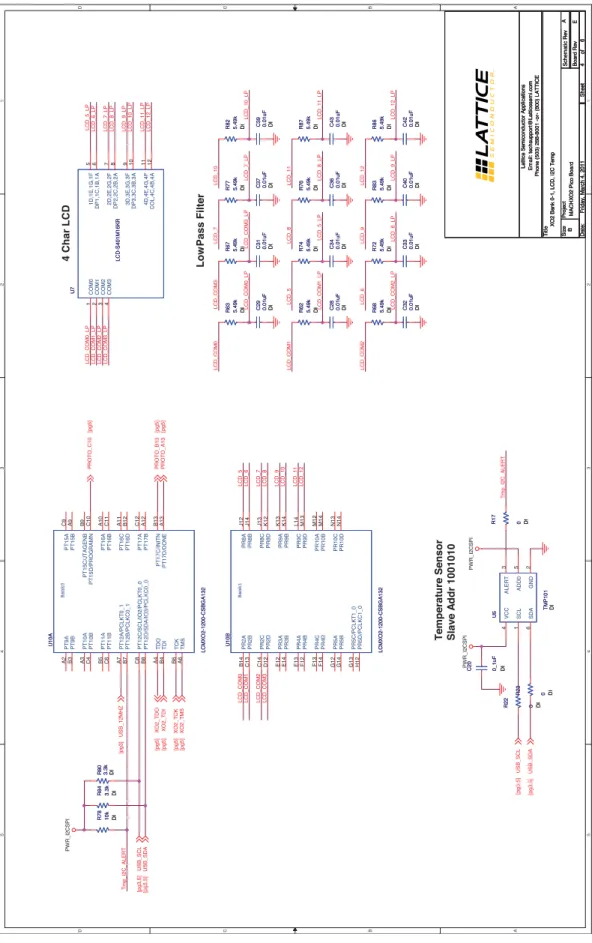
Figure 11. MachXO2 Banks 0-1, LCD, I2 C Temperature 5 5 4 4 3 3 2 2 1 1 D D C C B B A A Tm p_I 2 C _ ALER T LC D _C O M 0 LC D _C O M 1 LC D _C O M 2 LC D _C O M 3 LC D _5 LC D _6 LC D _9 LC D _10 LC D _11 LC D _12 LC D _7 LC D _8 L CD_ CO M 1 L CD_ CO M 0 L CD_ CO M 0 _ L P L CD_ CO M 1 _ L P L CD_ CO M 2 L CD_ CO M 2 _ L P LC D _ C O M 2_LP L CD_ CO M 3 _ L P LC D _7_LP LC D _8_LP LC D _5_LP LC D _6_LP LC D _11_LP LC D _12_LP LC D _9_LP LC D _10_LP L CD_ CO M 0 _ L P L CD_ CO M 1 _ L P Tm p _ I2 C_ AL ERT LC D _C O M 3 LC D _ C O M 3_LP LC D _5_LP LC D _6_LP LC D _5 LC D _6 LC D _7_LP LC D _7 LC D _10_LP LC D _10 LC D _11_LP LC D _12_LP LC D _11 LC D _12 LC D _8_LP LC D _8 LC D _9_LP LC D _9 PW R_ I2 CSPI PW R_ I2 CSPI PW R_ I2 CSPI USB_ SDA [pg3, 5] USB_ SCL [pg3, 5] XO 2 _ TDO [pg5] XO 2 _ TM S [pg5] XO 2 _ TCK [pg5] XO 2 _ TDI [pg5] U S B _12M H Z [pg3] USB_ SDA [pg3, 5] USB_ SCL [pg3, 5] P R OT O_ C 1 0 [p g 5 ] P R OT O_ B 1 3 [p g 5 ] P R OT O_ A 1 3 [p g 5 ] Da te : Si z e Sc h e m a ti c Re v of S h eet Ti tl e Lat ti c e S e m iconduct o r A p pl ic at io ns E m ai l: t e chsuppor t@ Lat ti ce se m i. c om P h one ( 5 03) 2688001 -o ( 8 00) LA TTI C E Bo a rd Re v Pr o je c t Fr iday, M ar c h 4, 2011 B 6 4 X O 2 B ank 0-1, LC D , I 2C Te m p M ACHXO 2 Pi c o Bo a rd E A Da te : Si z e Sc h e m a ti c Re v of S h eet Ti tl e Lat ti c e S e m iconduct o r A p pl ic at io ns E m ai l: t e chsuppor t@ Lat ti ce se m i. c om P h one ( 5 03) 2688001 -o ( 8 00) LA TTI C E Bo a rd Re v Pr o je c t Fr iday, M ar c h 4, 2011 B 6 4 X O 2 B ank 0-1, LC D , I 2C Te m p M ACHXO 2 Pi c o Bo a rd E A Da te : Si z e Sc h e m a ti c Re v of S h eet Ti tl e Lat ti c e S e m iconduct o r A p pl ic at io ns E m ai l: t e chsuppor t@ Lat ti ce se m i. c om P h one ( 5 03) 2688001 -o ( 8 00) LA TTI C E Bo a rd Re v Pr o je c t Fr iday, M ar c h 4, 2011 B 6 4 X O 2 B ank 0-1, LC D , I 2C Te m p M ACHXO 2 Pi c o Bo a rd E A Low Pass Fi lt er 4 Char LCD T e mper at ur e Sensor Sl av e A ddr 1001010 R1 7 0 DI R1 7 0 DI C3 2 0. 01uF DI C3 2 0. 01uF DI R8 7 5. 49k DI R8 7 5. 49k DI C4 0 0. 01uF DI C4 0 0. 01uF DI Bank0 L C M XO 2 -1 2 0 0 -CSBG A1 3 2 U1 0 A Bank0 L C M XO 2 -1 2 0 0 -CSBG A1 3 2 U1 0 A PT 9 A A2 PT 9 B B3 PT 1 0 A A3 PT 1 0 B C4 TD O A4 TD I B4 PT 1 1 A B5 PT 1 1 B C6 TC K B6 TM S A6 P T 12A /P C LK T 0_1 A7 P T 12B /P C LK C 0_1 B7 P T 12C /S C L/ IO 2/ P C LK T 0 _0 C8 PT 1 2 D/SDA/IO 3 /PCL K C0 _ 0 B8 PT 1 5 A C9 PT 1 5 B A9 PT15C/JTAGENB B9 P T 1 5 D/ P R OGRA M N C1 0 PT 1 6 A A1 0 PT 1 6 B C1 1 PT 1 6 C A1 1 PT 1 6 D B1 2 PT 1 7 A C1 2 PT 1 7 B A1 2 PT 1 7 C/INIT N B1 3 PT 1 7 D/DONE A1 3 C2 8 0. 01uF DI C2 8 0. 01uF DI C3 3 0. 01uF DI C3 3 0. 01uF DI R7 6 5. 49k DI R7 6 5. 49k DI R8 3 5. 49k DI R8 3 5. 49k DI C3 4 0. 01uF DI C3 4 0. 01uF DI R7 7 5. 49k DI R7 7 5. 49k DI R8 4 3. 3k DI R8 4 3. 3k DI C3 6 0. 01uF DI C3 6 0. 01uF DI R6 2 5. 49k DI R6 2 5. 49k DI C3 7 0. 01uF DI C3 7 0. 01uF DI R8 6 5. 49k DI R8 6 5. 49k DI R7 2 5. 49k DI R7 2 5. 49k DI R6 3 5. 49k DI R6 3 5. 49k DI R8 0 3. 3k DI R8 0 3. 3k DI U7 LC D -S 401M 16K R U7 LC D -S 401M 16K R COM 0 1 COM 1 2 COM 2 3 COM 3 4 1D ,1E ,1G ,1 F 5 D P 1, 1C ,1B ,1A 6 2D ,2E ,2G ,2 F 7 D P 2, 2C ,2B ,2A 8 3D ,3E ,3G ,3 F 9 D P 3, 3C ,3B ,3A 10 4D ,4E ,4G ,4 F 11 C O L, 4C ,4B ,4A 12 C2 9 0. 01uF DI C2 9 0. 01uF DI Bank1 L C M XO 2 -1 2 0 0 -CSBG A1 3 2 U1 0 B Bank1 L C M XO 2 -1 2 0 0 -CSBG A1 3 2 U1 0 B PR2 A B1 4 PR2 B C1 3 PR2 C C1 4 PR2 D D1 2 PR3 A E1 2 PR3 B E1 4 PR4 A E1 3 PR4 B F12 PR4 C F13 PR4 D F14 PR5 A G1 2 PR5 B G1 4 PR5 C /PCL KT 1 _ 0 G1 3 PR5 D /PCL KC1 _ 0 H1 2 PR8 A J12 PR8 B J14 PR8 C J13 PR8 D K1 2 PR9 A K1 3 PR9 B K1 4 PR9 C L14 PR9 D M1 3 PR1 0 A M1 2 PR1 0 B M1 4 PR1 0 C N1 3 PR1 0 D N1 4 C3 9 0. 01uF DI C3 9 0. 01uF DI R7 8 10k DI R7 8 10k DI U5 TM P101 DI U5 TM P101 DI VCC 4 GN D 2 ADD0 5 SCL 1 SDA 6 AL ERT 3 R8 2 5. 49k DI R8 2 5. 49k DI C2 0 0_1uF DI C2 0 0_1uF DI R2 2 0 DI R2 2 0 DI C4 3 0. 01uF DI C4 3 0. 01uF DI R7 4 5. 49k DI R7 4 5. 49k DI C3 1 0. 01uF DI C3 1 0. 01uF DI R2 3 0 DI R2 3 0 DI R6 8 5. 49k DI R6 8 5. 49k DI R6 7 5. 49k DI R6 7 5. 49k DI C4 2 0. 01uF DI C4 2 0. 01uF DI
Figure 12. MachXO2 Banks 2-3, Capacitor Pads, Expansion Header, SPI 4 4 3 3 2 2 1 1 D C B A Ca p B tn 2 Ca p B tn 1 Ca p B tn 3 Ca p B tn 4 Pu s h Bt n P R OT O_ K 1 P R OT O_ K 3 XO 2 _ SPI _ CL K XO 2 _ SPI _ O U T XO 2 _ SPI _ IN XO 2 _ SPI _ CS0 P R OT O_ B 1 P R OT O_ B 2 P R OT O_ C 1 P R OT O_ C 3 P R OT O_ C 2 P R OT O_ D 1 P R OT O_ M 7 P R OT O_ N 8 Ca p B tn 4 Ca p B tn 2 Pu s h Bt n PRO T O _ K1 PRO T O _ K3 PRO T O _ M 7 PRO T O _ N8 PRO T O _ B1 PRO T O _ B2 PRO T O _ C1 PRO T O _ C3 P R OT O_ C 2 PRO T O _ D1 XO 2 _ SPI _ IN XO 2 _ SPI _ CL K XO 2 _ SPI _ O U T XO 2 _ SPI _ CS0 X O 2_S P I_I N X O 2_S P I_C LK X O 2_S P I_O U T XO 2 _ SPI _ C S0 XO 2 _ SPI _ SN XO 2 _ SPI _ SN XO 2 _ SPI _ IN XO 2 _ SPI _ CL K XO 2 _ SPI _ O U T XO 2 _ SPI _ CS0 VCCI O _ EXT VCCI O _ EXT VCCI O _ EXT VCCI O _ EXT +3. 3 Vor B at PW R_ I2 CSPI DSVr e fVc c [p g 2 ] DSI n Vc c [p g 2 ] D S O u tV c c [p g 2 ] DSVr e fVc c o [p g 2 ] D S In V c c o [p g 2 ] D S Out V cco [pg2] En AM P [pg2] En I2 CSPI [pg2] BDBUS2 [p g 3 ] BDBUS3 [p g 3 ] BDBUS4 [p g 3 ] BDBUS5 [p g 3 ] BDBUS6 [p g 3 ] BDBUS7 [p g 3 ] BDBUS1 [p g 3 ] BDBUS0 [p g 3 ] X O 2_TD O [pg4] USB_ T D O [p g 3 ] USB_ T D I [p g 3 ] X O 2_TC K [pg4] X O 2_TM S [pg4] X O 2_TD I [pg4] USB_ T C K [p g 3 ] USB_ T M S [p g 3 ] USB_ SDA [p g 3 ,4 ] USB_ SCL [p g 3 ,4 ] PR OT O_ B 1 3 [p g 4 ] P R OT O_ A 1 3 [p g 4 ] P R OT O_ C 1 0 [p g 4 ] Da te : Si z e Sc h e m a ti c Re v of S h eet Ti tl e L a ttic e S e m ic o n d u c to r A p p lic a tio n s E m a il : t ec h s u p p o rt @ L a tt ic es em i. c o m P h one ( 5 03) 2688001 -o ( 8 00) LA TTI C E B oar d R e v Pr o je c t Fr iday, M ar c h 4, 2011 B 6 5 X O 2 B a nk 2-3, C a p P a ds, E x pansi on H e ade r, S P I M ACHXO 2 Pi c o Bo a rd E A Da te : Si z e Sc h e m a ti c Re v of S h eet Ti tl e L a ttic e S e m ic o n d u c to r A p p lic a tio n s E m a il : t ec h s u p p o rt @ L a tt ic es em i. c o m P h one ( 5 03) 2688001 -o ( 8 00) LA TTI C E B oar d R e v Pr o je c t Fr iday, M ar c h 4, 2011 B 6 5 X O 2 B a nk 2-3, C a p P a ds, E x pansi on H e ade r, S P I M ACHXO 2 Pi c o Bo a rd E A Da te : Si z e Sc h e m a ti c Re v of S h eet Ti tl e L a ttic e S e m ic o n d u c to r A p p lic a tio n s E m a il : t ec h s u p p o rt @ L a tt ic es em i. c o m P h one ( 5 03) 2688001 -o ( 8 00) LA TTI C E B oar d R e v Pr o je c t Fr iday, M ar c h 4, 2011 B 6 5 X O 2 B a nk 2-3, C a p P a ds, E x pansi on H e ade r, S P I M ACHXO 2 Pi c o Bo a rd E A v e T ouch Pads GSR/Wake fr
om Standby Part Number:EVQ Q2K03W Panasonic SMD
Header Pac k age: SOIC8 (W IDE) Pa c k ag e: UDFN 4MBi t SPI
(Refer to Appendix D. Limitations)
U1 2 Ca p T o u c h U1 2 Ca p T o u c h Ca p B tn 1 R9 3 100k DNI R9 3 100k DNI R3 3 0 DI R3 3 0 DI Bank2 LC M X O 2- 1200-C S B G A 1 32 U1 0 C Bank2 LC M X O 2- 1200-C S B G A 1 32 U1 0 C PB2 0 D/SI/SISPI/IO 0 P1 3 PB2 0 C/SN N1 2 PB2 0 B P1 2 PB2 0 A M1 1 PB1 8 D P1 1 PB1 8 C M1 0 PB1 8 B N1 0 PB1 8 A M9 PB1 5 D N9 PB1 5 C P9 PB1 5 B M8 PB1 5 A P8 PB1 1 B/PCL K C2 _ 1 N8 PB1 1 A/PCL K T 2 _ 1 M7 PB1 1 D N7 PB1 1 C P7 PB9 B /PCL KC2 _ 0 P6 PB9 A /PCL KT 2 _ 0 N6 PB9 D M5 PB9 C N5 PB6 D /SO /SPISO/IO1 N4 PB6 C /M CL K/CCL K M4 PB6 B P4 PB6 A N3 PB4 D M3 PB4 C /CSSPIN P3 PB4 B N2 PB4 A P2 C4 8 0. 1uFDNI C4 8 0. 1uFDNI R3 7 6 8 DI R3 7 6 8 DI C5 0 0. 1uFDNI C5 0 0. 1uFDNI U3 HEADER 1 6 X2 U3 HEADER 1 6 X2 2 4 6 8 10 12 14 16 18 20 22 24 26 28 30 1 3 5 7 9 11 13 15 17 19 21 23 25 27 29 31 32 R4 4 10k DI R4 4 10k DI R4 8 0 DI R4 8 0 DI U1 3 Ca p T o u c h U1 3 Ca p T o u c h Ca p Btn 1 C1 0 0_1uF DI C1 0 0_1uF DI S1 G lo b a lR es et PCB Fo o tp ri n t = SM T_ SW DI S1 G lo b a lR es et PCB Fo o tp ri n t = SM T_ SW DI 1 4 2 3 R7 0 0 DI R7 0 0 DI U9 AT 25D F 041A -S H -B U9 AT 25D F 041A -S H -B S 1 Q 2 W 3 Vs s 4 Vc c 8 D 5 C 6 Re s e t 7 R2 5 10k DI R2 5 10k DI u c h u c h U1 7 A T 25D F 041A -M H U1 7 A T 25D F 041A -M H S 1 Q 2 W 3 Vs s 4 Vc c 8 D 5 C 6 Re s e t 7 R6 9 0 DI R6 9 0 DI C1 1 0. 1uFDI C1 1 0. 1uFDI u c h u c h R7 1 0 DI R7 1 0 DI R2 0 DI R2 0 DI R9 0 100k DNI R9 0 100k DNI Bank3 LC M X O 2- 1200-C S B G A 1 32 U1 0 D Bank3 LC M X O 2- 1200-C S B G A 1 32 U1 0 D PL 1 0 D M2 PL 1 0 C M1 PL 1 0 B L3 PL 9 B /PCL KC3 _ 0 K3 PL 9 A /PCL KT 3 _ 0 K1 PL 8 D K2 PL 8 C J3 PL 8 B J2 PL 8 A J1 PL 5 D H3 PL 5 C H1 PL 5 B /PCL KC3 _ 1 H2 PL 5 A /PCL KT 3 _ 1 G3 PL 4 D F3 PL 4 C F1 PL 4 B F2 PL 4 A E3 PL 3 D E2 PL 3 C E1 PL 3 B /PCL KC3 _ 2 D1 PL 3 A /PCL KT 3 _ 2 C2 PL 2 D /L _ G PL L C _ IN C3 PL 2 C /L _ G PL L T _ IN C1 PL 2 B/L _ G PL L C _ F B B2 P L2A /L_G P L LT _FB B1 R3 2 0 DI R3 2 0 DI R9 5 0 DI R9 5 0 DI R6 6 0 DI R6 6 0 DI
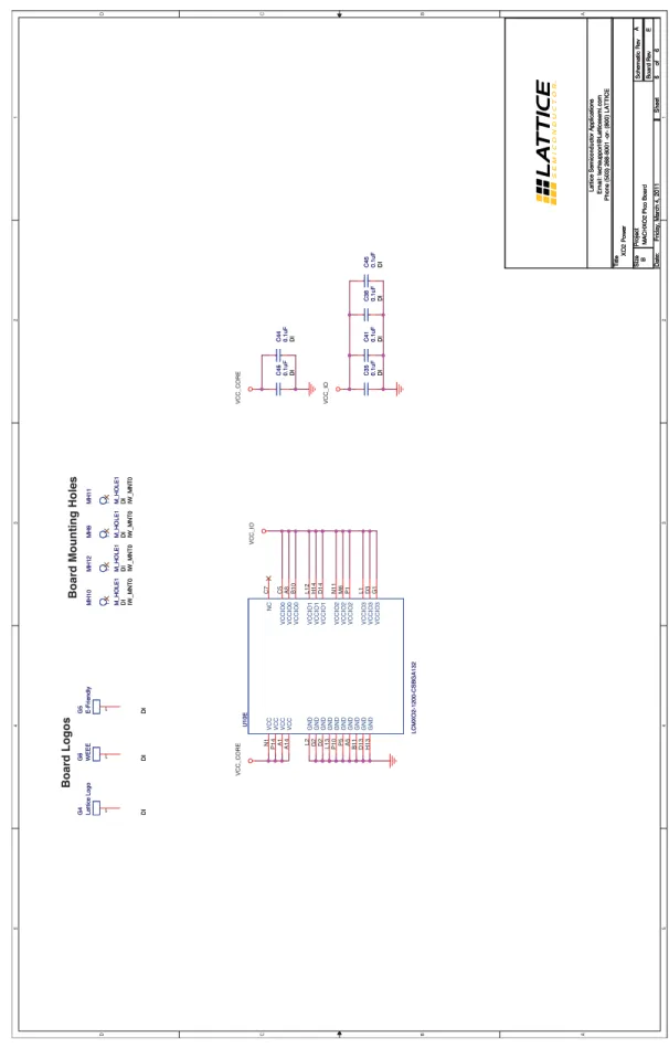
Figure 13. MachXO2 Power 5 5 4 4 3 3 2 2 1 1 D D C C B B A A VCC_ IO VCC_ CO RE VCC_ CO RE VCC_ IO Da te : Si z e Sc h e m a ti c Re v of S h eet Ti tl e Lat ti c e S e m iconduct o r A p pl ic at io ns E m ai l: t e chsuppor t@ Lat ti ce se m i. c om P hone ( 5 03) 2688001 -o ( 8 00) LA TTI C E B oar d R e v Pr o je c t Fr iday, M ar c h 4, 2011 B 6 6 XO 2 Po we r M ACHXO 2 Pi c o Bo a rd E A Da te : Si z e Sc h e m a ti c Re v of S h eet Ti tl e Lat ti c e S e m iconduct o r A p pl ic at io ns E m ai l: t e chsuppor t@ Lat ti ce se m i. c om P hone ( 5 03) 2688001 -o ( 8 00) LA TTI C E B oar d R e v Pr o je c t Fr iday, M ar c h 4, 2011 B 6 6 XO 2 Po we r M ACHXO 2 Pi c o Bo a rd E A Da te : Si z e Sc h e m a ti c Re v of S h eet Ti tl e Lat ti c e S e m iconduct o r A p pl ic at io ns E m ai l: t e chsuppor t@ Lat ti ce se m i. c om P hone ( 5 03) 2688001 -o ( 8 00) LA TTI C E B oar d R e v Pr o je c t Fr iday, M ar c h 4, 2011 B 6 6 XO 2 Po we r M ACHXO 2 Pi c o Bo a rd E A Boar d Logos Boar d Mount ing Hol e s G4 Lat ti c e Logo DI G4 Lat ti c e Logo DI 1 C4 1 0. 1uF DI C4 1 0. 1uF DI G5 E-F rie n d ly DI G5 E-F rie n d ly DI 1 C4 6 0. 1uF DI C4 6 0. 1uF DI G6 WE E E DI G6 WE E E DI 1 MH 1 0 M_ H O L E 1 DI IW _ M N T 0 MH 1 0 M_ H O L E 1 DI IW _ M N T 0 1 C3 5 0. 1uF DI C3 5 0. 1uF DI MH 9 M_ H O L E 1 DI IW _ M N T 0 MH 9 M_ H O L E 1 DI IW _ M N T 0 1 C4 4 0. 1uF DI C4 4 0. 1uF DI MH 1 1 M_ H O L E 1 DI IW _ M N T 0 MH 1 1 M_ H O L E 1 DI IW _ M N T 0 1 MH 1 2 M_ H O L E 1 DI IW _ M N T 0 MH 1 2 M_ H O L E 1 DI IW _ M N T 0 1 LC M X O 2- 1200-C S B G A 1 32 U1 0 E LC M X O 2- 1200-C S B G A 1 32 U1 0 E GN D L2 GN D G2 GN D D2 GN D B1 1 GN D D1 3 GN D H1 3 VCC P1 4 VCC A1 NC C7 GN D A5 VCC A1 4 GN D L13 GN D P1 0 GN D P5 VCC N1 VCCIO 0 C5 VCCIO 0 A8 VCCIO 0 B1 0 VCCIO 1 L12 VCCIO 1 H1 4 VCCIO 1 D1 4 VCCIO 2 N1 1 VCCIO 2 M6 VCCIO 2 P1 VCCIO 3 L1 VCCIO 3 D3 VCCIO 3 G1 C3 8 0. 1uF DI C3 8 0. 1uF DI C4 5 0. 1uF DI C4 5 0. 1uF DI
Appendix B. Bill of Materials
Item Quantity Reference Part Footprint Populate Vendor Part Number Description
1 2 C10,C20 0_1uF SM/C_0603 DI Panasonic ECJ-1VB1C104K 0.1uF surface mount cap
2 3 C1,C2,C21 1uF SM/C_0603 DI Panasonic ECJ-2YB1A105K 1uF surface mount cap
3 2 C5,C6 10nF SM/C_0603 DI Panasonic ECG ECJ-1VB1C104K 10nF SMC
4 1 J1 USB_MINI_B TYPE_B DI Hirose UX60-MB-5ST USBType-BMiniConnector
5 35 R2,R8,R11,R13,R14,R15,R1 6,R17,R20,R21,R22,R23,R31 ,R32,R33,R34,R35,R40,R43, R47,R48,R49,R55,R56,R64, R65,R66,R69,R70,R71,R75, R89,R95,R96,R97
0 SM/R_0603 DI Panasonic ECG ERJ-3GEY0R00V Resistor 0.0 SMD 0603
6 5 R50,R58,R60,R79,R92 1k SM/R_0603 DI Vishay/Dale CRCW06031K00FKEA Resistor 1k SMD 0603
7 8 R1,R3,R4,R25,R27,R29,R44,
R78
10k SM/R_0603 DI Vishay/Dale CRCW060310K0FKEA 10K 0603 SMT resistor
8 1 R59 10k SM/R_0603 DNI Vishay/Dale CRCW060310K0FKEA 10K 0603 SMT resistor
9 1 U1 M93C46-WMN6TP SOIC-8 DI STMicroelectronics M93C46-WMN6TP IC 1K EEPROM 8-SOIC
10 1 U5 TMP101 SM/SOT23_6 DI TI TMP101NA/250 IC TEMP SENSOR DIG
SOT-23-6
11 1 R19 1M SM/R_0603 DI PanasonicECG ERJ-3GEYJ105V RES 1.0M1/10W5%
12 1 R53 1M SM/R_0603 DNI PanasonicECG ERJ-3GEYJ105V RES 1.0M1/10W5%
13 1 U17 AT25DF041A-MH UDFN DNI Atmel AT25DF041A-MH IC FLASH 4MBIT 70MHZ
8SOIC
14 4 MH9,MH10,MH11,MH12 M_HOLE1 IW_MNT0 DI 3M SJ-5003 (BLACK) BUMPON HEMISPHERE
.44X.20 BLACK
15 6 R38,R42,R46,R51,R57,R61 2k SM/R_0603 DI Susumu Co Ltd RG1608P-202-B-T5 RES 2.0K OHM 1/10W .1%
0603 SMD
16 1 BT1 Batt_Cell_Holder BA2032_Battery_
Holder
DI Linx Technologies Inc BAT-HLD-001 HOLDER BATTERY 20MM
COIN CR2032
17 16 C3,C9,C11,C12,C24,C25,C2
6,C35,C38,C41,C44,C45,C46 ,C54,C57,C58
0.1uF SM/C_0603 DI TDK Corporation C1608X7R1E104K CAP CER .10UF 25V X7R
10% 0603
18 4 C47,C48,C49,C50 0.1uF SM/C_0603 DNI TDK Corporation C1608X7R1E104K CAP CER .10UF 25V X7R
10% 0603
19 12 C28,C29,C31,C32,C33,C34,
C36,C37,C39,C40,C42,C43
0.01uF SM/C_0603 DI TDK Corporation C1608X7R1H103K CAP CER 10000PF 50V
X7R 10% 0603
20 1 C23 0.33uF SM/C_0603 DI TDK Corporation C1608X7R1A334K CAP CER .33UF 10V X7R
0603
21 1 C7 6.8uF SM/C_1206 DI AVX Corporation TAJA685K020RNJ CAP TANTALUM 6.8UF
20V 10% SMD
22 1 C8 10uF SM/C_0805 DI Nichicon TAJA685K020RNJ CAP TANTALUM 10UF
6.3V 20% SMD
23 1 D2 Blue SM/D_0603 DI Lite-On Inc LTST-C190TBKT LED 468NM BLUE CLEAR
0603 SMD
24 1 L1 Ferrite_bead SM/R_0603 DI Laird-Signal Integrity
Products
MI0603J600R-00 FERRITE 1A 60 OHM
0603 SMD
25 1 U2 MCP1703T-1202E/CB SOT-23A-3 DI Microchip Technology MCP1703T-1202E/CB IC REG LDO 1.2V 200MA
SOT-23A
26 3 R5,R7,R28 100k SM/R_0603 DI Panasonic - ECG ERJ-3GEYJ104V RES 100K OHM 1/10W 5%
0603 SMD
27 4 R88,R90,R93,R94 100k SM/R_0603 DNI Panasonic - ECG ERJ-3GEYJ104V RES 100K OHM 1/10W 5%
32 1 R98 12k SM/R_0603 DI Panasonic - ECG ERA-3AEB123V RES 12K OHM 1/10W .1% 0603 SMD
33 3 Q1,Q3,Q4 IRLML6402PbF SM/SOT23_123 DI International Rectifier IRLML6402TRPBF MOSFET P-CH 20V 3.7A
SOT-23
34 1 Q2 IRF240 SM/SOT23_123 DI International Rectifier IRLML2502TRPBF MOSFET N-CH 20V 4.2A
SOT-23
35 1 S1 GlobalReset SMT_SW DI Panasonic - ECG EVQ-Q2K03W SWITCH LT 6MM 130GF
H=3.1MM SMD
36 1 U8 NCP1117
SOT-223_checkpins
DI STMicroelectronics NCP1117ST33T3G IC REG LDO 1A 3.3V
SOT223
37 1 U3 HEADER 16X2 Header16x2 DNI Samtec Inc TLW-108-06-G-D CONN HEADER .100"
16POS DL GOLD
38 2 C19,C30 0.047uF SM/C_0603 DI TDK Corporation C1608X7R1H473K CAP CER 47000PF 50V
X7R 10% 0603
39 2 R18,R85 1 SM/R_0603 DI Vishay/Dale CRCW06031R00FKEA RES 1.00 OHM 1/10W 1%
0603 SMD
40 1 D3 NSR0530P2T5G SM/SOD_923 DNI ON Semiconductor NSR0530P2T5G DIODE SCHOTTKY 30V
0.5A SOD-923
41 1 R24 20 SM/R_0603 DNI Panasonic - ECG ERJ-3GEYJ200V RES 20 OHM 1/10W 5%
0603 SMD
42 2 R80,R84 3.3k SM/R_0603 DI Rohm Semiconductor MCR03EZPJ332 RES 3.3K OHM 1/10W 5%
0603 SMD
43 1 R36 3.3k SM/R_0603 DNI Rohm Semiconductor MCR03EZPJ332 RES 3.3K OHM 1/10W 5%
0603 SMD
44 1 U10 LCMXO2-1200-CSBGA132 CSBGA132 DI Lattice
LCMXO2-1200-CSBGA132 LCMXO2-1200-CSBGA132 45 1 U7 LCD-S401M16KR LCD-S401M16KR DI Lumex Opto/Components Inc
LCD-S401M16KR LCD custom order from
phil@duerfeldtengineering. com
46 12 R62,R63,R67,R68,R72,R74,
R76,R77,R82,R83,R86,R87
5.49k SM/R_0603 DI Panasonic - ECG ERJ-3EKF5491V RES 5.49K OHM 1/10W
1% 0603 SMD
47 1 R37 68 SM/R_0603 DI Panasonic - ECG ERJ-3GEYJ680V RES 68 OHM 1/10W 5%
0603 SMD
48 2 C55,C56 18pF SM/C_0603 DI TDK Corporation C1608C0G1H180J CAP CER 18PF 50V C0G
5% 0603
49 1 C51 3.3uF SM/C_0603 DI TDK Corporation C1608X5R0J335K CAP CER 3.3UF 6.3V X5R
0603
50 1 C13 4.7uF SM/C_0603 DI TDK Corporation C1608X5R0J475K CAP CER 4.7UF 6.3V X5R
0603
51 1 L3 600ohm 500mA FB0603 DI Murata Electronics North
America
BLM18AG601SN1D FERRITE CHIP 600 OHM
500MA 0603
52 1 U23 FT2232HL tqfp64_0p5_12p2
x12p2_h1p6
DI Future FT2232H R USB UART/FIFO
53 1 X3 12MHZ crystal_4p_3p2x2
p5
DI TXC CORPORATION 7M-12.000MAAJ-T CRYSTAL 12.000 MHZ
18PF SMD
54 3 U20,U21,U22 STG3693QTR QFN DI STMicroelectronics STG3693QTR IC SWITCH QUAD SPDT
16QFN
55 1 U15 LMP7708 MSOP DI STMicroelectronics LMP7708MM/NOPB IC AMP PREC R-R OUT
DUAL 8-MSOP
56 2 C22,C27 220pF SM/C_0603 DI TDK Corporation C1608X7R1H221K CAP CER 220PF 50V X7R
10% 0603
57 1 U9 AT25DF041A-SH-B
AT25DF041A-SOIC-8
DI Atmel AT25DF041A-SH-B IC FLASH 4MBIT 70MHZ
8SOIC
58 1 G4 Lattice Logo LOGO300_1000 DI
59 1 G5 E-Friendly EFRIENDLY_400
_SM
DI
60 1 G6 WEEE WEEE_SM DI
61 4 TP1,TP2,TP3,TP4 TP LOGO300_1000 DI
62 4 U11,U12,U13,U14 CapTouch CapTouch
Appendix C. SPI Programming
• In order to support SPI programing of the MachXO2 device the zero ohm resistors (R71, R70, R66, R69) will have to be removed
• Once removed, the SPI programming pins can be accessed via the header U3 (XO2_SPI_OUT, XO2_SPI_IN, XO2_SPI_CLK, XO2_SPI_SN)
Appendix D. Dual Boot Demonstration
You can demonstrate MachXO2 dual boot using the MachXO2 Pico Evaluation Board. Before you start you will need to do the following:
1. Create a SVF file to erase only the Configuration Flash and UFM memory. Do NOT erase the Feature Row.
a. Use ispVM or Diamond Programmer to create a SVF file with the which erases the device as a base-line.
b. Modify your SVF to change the following: ! Shift in ISC ERASE(0x0E) instruction
SIR 8 TDI (0E);
SDR 8 TDI (0C); ! Change from E=1110 to C=1100 no Feature Row
c. For more information on the Feature Row, refer to TN1204, MachXO2 Programming and Configuration
Usage Guide.
2. Update the MachXO2 Pico Demo to enable dual boot.
a. Using Diamond in the Spreadsheet View, Global Preference tab set MASTER_SPI_PORT=ENABLE. 3. Power-on the SPI memory on the MachXO2 Pico Evaluation Board.
a. This is a low power board and if something is not used it is powered down. This can done by shorting the south side of C25 and R97 by soldering or holding a probe on them as they are beside each other. For reference, the north side of the board has the header U3. Shorting these components provides sets the mux U21 select high powering up the SPI device.
b. For more information, refer to the board schematics in “Appendix A. Schematic” on page 10.
Figure 14. MachXO2 Pico Evaluation Board SPI/I2
C Bus Power Enable
R96
U21 C25 R97
Demonstrating Dual Boot
1. Program the MachXO2 device with the modified Pico Demo.
a. Select the operation Flash Erase, Program, Verify. b. “PICO” will display on the LCD showing that it is running.
a. Using ispVM or Diamond Programmer the SPI Flash can be programmed with the SPI Flash Program-ming option.
b. As defined in TN1204, MachXO2 Programming and Configuration Usage Guide, the starting address
must be 0x010000.
3. Reprogram the MachXO2 device with the modified Pico Demo as the Feature Row was erased when the SPI was programmed.
4. Erase the MachXO2 Flash (and not the Feature Row) using the modified SVF file.
5. Power cycle and watch dual boot in action as the MachXO2 loads the image from the SPI into the SRAM. a. “PICO” will display on the LCD showing that it is running.
Appendix E. Limitations
• Pin A7 USB_12MHz clock should be an input unless R31 is removed to ensure FTDI device operation • Pin B9 JTAGENB is not connected on the board


![Figure 10. USB to JTAG and I 2 C for the MachXO2 4 4332211DCBA EESK EEDATA HLD_Debug EECSSB+3.3V+3.3VorBat+3.3VVCC18FT+3.3V+3.3V+3.3V PWR_ENABLEb[pg1]](https://thumb-us.123doks.com/thumbv2/123dok_us/775157.2598029/12.918.158.763.133.1073/figure-jtag-machxo-eedata-debug-eecssb-vorbat-enableb.webp)