MODULATING OPTICAL AND ELECTRONIC PROPERTIES IN SILICON
NANOWIRE SUPERLATTICES
David John Hill
A dissertation submitted to the faculty of the University of North Carolina at Chapel Hill in
partial fulfillment of the requirements for the degree of Doctor of Philosophy in the Department
of Chemistry.
Chapel Hill
2018
Approved by:
James F. Cahoon
Joanna M. Atkin
Scott C. Warren
Frank A. Leibfarth
ABSTRACT
David John Hill: Modulating Optical and Electronic Properties in Silicon Nanowire Superlattices
(Under the direction of James F. Cahoon)
Here, we develop new techniques for implementing silicon nanowires (NWs) in complex photonic
and electronic applications. First, we present waveguide scattering microscopy (WSM) as an alternative
technique to dark-field microscopy (DFM) to image and analyze photonic nanostructures. WSM uses a
white-light source coupled to a dielectric slab waveguide to generate an evanescent field that illuminates
objects on the waveguide surface. We demonstrate high-contrast dark-field imaging of nanophotonic and
plasmonic structures such as Si nanowires, Au nanorods, and Ag nanoholes. Scattering spectra collected
in the WSM configuration show excellent signal-to-noise with minimal background signal compared
to conventional DFM. In addition, the polarization of the incident field is controlled by the direction of
the propagating wave, providing a straightforward route to excite specific optical modes in anisotropic
nanostructures.
We also overcome several difficulties of VLS NW growth, such as nonselective deposition, kinking,
and compositional gradients, and report the synthesis of uniform, linear, and degenerately doped Si NW
superlattices. The synthesis is enabled by
in situ
chlorination of the NW surface with hydrochloric acid.
We find the boron doping level to far exceed the solid solubility limit, resulting from crystallization
kinetics. Because the boron and phosphorus doping levels are degenerate, both segments inhibit the
etching of Si in basic solutions. Moreover, we find that the dopant transitions are abrupt, facilitating
morphological control with a spatial resolution of
∼
10 nm.
We delineate how the photovoltaic performance of NWs with axial
p-i-n
junctions is dictated
not simply by the surface but also by the complex interplay of diode geometry - i.e. radius (
R
) and
intrinsic length (
L
i) - with the surface recombination velocity (
S
). Using a combination of finite-element
simulations, analytical theory, and single-NW measurements, we evaluate the dependence of the dark
saturation current (
I
o), internal quantum efficiency (IQE), short-circuit current (
I
SC), and open-circuit
ACKNOWLEDGEMENTS
I am in an immeasurable debt to my family, especially my parents Ken and Judy, my sisters Alicia
and Megan, and all of my grandparents, for their love and support during this process and throughout my
life. I am often unwilling or unable to express what I am feeling, but you have my gratitude for standing
by me through the good and the bad. Cedar, we miss you dearly.
I would also like to thank my advisor Jim Cahoon for providing guidance and mentoring over my
many years here. When I came to UNC, I didn’t even know what a semiconductor was, and I have learned
an immeasurable amount in that time. I would also like to thank him for putting up with my jokes and
treating my opinions as worthwhile.
I would like to thank current and former members of the Cahoon lab, among whom I count many
friends, for their help in the lab and outside of it, for teaching me and allowing me to teach, and for being
with me there in the trenches.
TABLE OF CONTENTS
LIST OF TABLES . . . .
x
LIST OF FIGURES . . . .
xi
LIST OF ABBREVIATIONS . . . xiii
1
INTRODUCTION . . . .
1
1.1
Semiconductor Properties . . . .
1
1.1.1
Semiconductor Doping . . . .
2
1.1.2
Semiconductors and Light . . . .
3
1.2
Semiconductor Applications . . . .
4
1.2.1
Photovoltaics and Photodetectors . . . .
4
1.2.2
Light Emitting Diodes . . . .
5
1.2.3
Computation . . . .
6
1.3
Nanomaterials . . . .
6
1.3.1
Optical Properties of Nanomaterials . . . .
6
1.3.2
Electronic Properties of Nanomaterials . . . .
7
1.3.3
Semiconductor Nanowires . . . .
7
1.3.3.1
Nanowire Synthesis . . . .
8
1.3.3.2
Non-Equilibrium Processes . . . 15
1.3.3.3
Nanowire Photonics . . . 16
1.3.3.4
Nanowire Photovoltaics . . . 17
2
METHODS . . . 20
2.1.1
Substrate Preparation . . . 20
2.1.2
420°C Conditions . . . 21
2.1.3
510°C Conditions . . . 21
2.1.4
650°C Conditions . . . 22
2.2
Nanowire Etching . . . 22
2.3
Imaging . . . 23
2.3.1
Transition Width Fitting . . . 24
2.4
Spectroscopy . . . 25
2.5
Simulations . . . 26
2.5.1
Optical Simulations . . . 26
2.5.2
Electrostatic Simulations . . . 26
2.6
Microfabrication . . . 27
2.6.1
Marker Pattern Fabrication . . . 27
2.6.2
Nanowire Contact Fabrication . . . 28
2.6.3
Nanohole Fabrication . . . 30
2.6.4
PCB Fabrication . . . 30
2.7
Device Measurement . . . 30
2.7.1
IV Measurement. . . 30
2.7.2
Four-Point Probe . . . 31
2.7.3
EQE Measurement . . . 31
2.7.4
AFM Measurements . . . 32
3
WAVEGUIDE SCATTERING MICROSCOPY FOR DARK-FIELD IMAGING
AND SPECTROSCOPY OF PHOTONIC NANOSTRUCTURES . . . 33
3.1
Introduction. . . 33
3.2
Results and Discussion . . . 34
3.2.1
Plasmonic Nanoparticle Spectroscopy . . . 37
3.2.2
Dielectric Nanowire Scattering Spectroscopy . . . 40
3.3
Waveguide Photovoltaics . . . 45
3.4
Conclusions. . . 47
4
ENCODING HIGHLY NONEQUILIBRIUM BORON CONCENTRATIONS AND
ABRUPT MORPHOLOGY IN P-TYPE/N-TYPE SILICON NANOWIRE SUPERLATTICES
48
4.1
Introduction. . . 48
4.2
Results and Discussion . . . 50
4.2.1
p-Type Etching . . . 52
4.2.2
p-Type Doping Level . . . 54
4.2.3
ENGRAVE Morphology in p-Type and n-Type NWs . . . 60
4.3
Conclusions. . . 61
5
INTERPLAY OF SURFACE RECOMBINATION AND DIODE GEOMETRY FOR
THE PERFORMANCE OF AXIAL
P-I-N
NANOWIRE SOLAR CELLS . . . 62
5.1
Introduction. . . 62
5.2
Results and Discussion . . . 64
5.2.1
Theoretical Analysis . . . 64
5.2.2
Experimental Comparison . . . 75
5.3
Conclusions. . . 82
6
CONCLUSIONS . . . 84
LIST OF TABLES
4.1
Resistivity Measurements of p-type NWs . . . 56
5.1
Comparison of experimental and simulated photovoltaic metrics for as-grown and
oxidized/annealed axial
p-i-n
NWs measured in the dark and under simulated
LIST OF FIGURES
1.1
P-N junction . . . .
2
1.2
Solar cell
I-V
characterization . . . .
5
1.3
Top-down fabrication methods . . . .
9
1.4
Bottom-up synthesis methods . . . 11
1.5
Nanowire structures . . . 13
1.6
ENGRAVE process . . . 15
2.1
Waveguide scattering microscopy experimental setup . . . 23
2.2
Halogen lamp spectra for DFM and WSM . . . 24
2.3
Marker pattern . . . 28
2.4
Nanowire contacts . . . 29
3.1
Comparison of conventional DFM and WSM . . . 36
3.2
Geometry of the coverslip for C-WSM . . . 37
3.3
Surface Sensitivity of WSM . . . 38
3.4
Comparison of scattering spectra from plasmonic nanorods acquired with DFM and WSM . . 39
3.5
Cross-sectional view of plasmon resonances in Au nanorods . . . 40
3.6
Comparison of Mie scattering spectra from Si NWs acquired with DFM and WSM . . . 41
3.7
Polarization-selective illumination of Si NWs with WSM . . . 43
3.8
Directional coupling into the waveguide to control the wavevector . . . 43
3.9
Polarization-selective illumination of plasmonic Ag nanohole arrays with WSM . . . 44
3.10 Polarization of WSM . . . 45
3.11 Waveguide Photovoltaics . . . 46
4.1
p-type NW growth conditions . . . 50
4.2
Production of multiply chlorinated silanes . . . 51
4.4
p-type NW electrical transport properties . . . 54
4.5
EELS Characterization . . . 57
4.6
XPS Characterization . . . 57
4.7
EDS Characterization . . . 58
4.8
p-type ENGRAVE NWs . . . 60
4.9
Abrupt dopants and morphology in p-type and n-type NWs . . . 61
5.1
Simulated
I-V
characteristics of axial
p-i-n
NW devices . . . 64
5.2
Radiative and non-radiative recombination . . . 67
5.3
Comparison of simulated and analytical PV metrics . . . 68
5.4
Geometry-dependent photocurrent and IQE . . . 69
5.5
The effect of
L
ion PV metrics . . . 71
5.6
Geometrical effects on
V
OCand n determined by finite-element simulations . . . 73
5.7
Electron and hole concentration in the
p-i-n
junction . . . 74
5.8
Effect of geometry and
S
on
F F
. . . 75
5.9
Geometrically-defined and degenerately-doped axial
p-i-n
NWs . . . 76
5.10 Axial
p-i-n
single-NW PV devices . . . 78
5.11 PV performance at various illumination intensities after device oxidation and annealing . . . 79
5.12 Etched
p-i-n
photodiode . . . 81
5.13 Dark
I-V
curve of etched
p-i-n
device . . . 82
5.14 Polarization-resolved EQE spectra . . . 82
6.1
Avalanche photodiode . . . 87
LIST OF ABBREVIATIONS
A
area
AAO
anodic aluminum oxide
AFM
atomic force micropscopy
B
radiative recombination coefficient
BHF
buffered hydrofluoric acid
B-DFM
back-scattering dark-field microscopy
CVD
chemical vapor deposition
C-WSM
coverslip waveguide scattering microscopy
DFM
dark-field microscopy
D
ndiffusion constant for electrons
D
pdiffusion constant for holes
D
p,ndiffusion constants for electrons and holes
D
Πdistribution of surface trap state energies
EBL
electron-beam lithography
EDS
energy-dispersive x-ray spectroscopy
EELS
electron energy loss spectroscopy
E
iintrinsic Fermi level energy
ENGRAVE Encoded Nanowire GRowth and Appearance through VLS and Etching
E
Ttrap state energy
EQE
external quantum efficiency
FDFD
finite-difference frequency domain
FET
field-effect transistor
FF
fill factor
FIB
focused ion beam
F-DFM
forward-scattering dark-field microscopy
FWHM
full width at half maximum
I
current
I
odark saturation current
IPA
isopropyl alcohol
IQE
internal quantum efficiency
IR
infrared
I
SCshort-circuit current
I-V
current-voltage
J
SCshort-circuit current density
J
SCidealideal short-circuit current density
k
BBoltzmann constant
LED
light-emitting diode
L
iintrinsic segment length
L
nelectron effective diffusion length
L
n,pelectron and hole effective diffusion lengths
L
phole effective diffusion length
MFPL
mean-free path length
MIBK
methyl isobutyl ketone
MMA
methyl methacrylate
MOSFET
metal-oxide-semiconductor field effect transistor
n
electron concentration
n
ideality factor
N
A,Ddoping level
n
Delectron concentration in the depletion region
n
iintrinsic carrier concentration
NP
nanoparticle
NPGS
Nanometer Pattern Generation System
NR
nanorod
NW
nanowire
p
hole concentration
Φ
IQEspatially-dependent internal quantum efficiency
P
maxmaximum power
PML
perfectly matched layer
PMMA
poly(methyl methacrylate)
PV
photovoltaic
QD
quantum dot
R
nanowire radius
R
Drecombination rate in the depletion region
R
Ssurface recombination rate
R
Seriesseries resistance
R
SHshunt resistance
R
SRHShockley-Read-Hall recombination rate
S
surface recombination velocity
sccm
standard cubic centimeters per minute
SEM
scanning electron microscope
S
nelectron surface recombination velocity
S
phole surface recombination velocity
SRH
Shockley-Read-Hall
SRV
surface recombination velocity
STEM
scanning transmission electron microscope
s-SNOM
scattering-scanning near-field optical microscopy
S-WSM
substrate waveguide scattering microscopy
T
temperature
TE
transverse electric
TEM
transmission electron microscope
TIRFM
total internal reflection fluorescence microscopy
TIRM
total internal reflection microscopy
TM
transverse magnetic
τ
SRHShockley-Read-Hall recombination time
τ
SRH,nelectron Shockley-Read-Hall recombination time
τ
SRH,phole Shockley-Read-Hall recombination time
UV
ultraviolet
V
voltage
V
OCopen-circuit voltage
˜
V
OCnormalized open-circuit voltage
VLS
vapor-liquid-solid
VS
vapor-solid
VSS
vapor-solid-solid
WSM
waveguide scattering microscopy
W
Ddepletion width
WZ
wurtzite
INTRODUCTION
“Happy the Man, who, studying Nature’s Laws, Thro’ known Effects can trace the secret
Cause”
- John Dryden,
The Works of Virgil
1.1
Semiconductor Properties
Semiconducting materials form the basis for most modern electronic devices, largely due to the ways
in which they can be modified. Semiconductor doping allows for modification of the material’s electronic
properties, changing its carrier density, disrupting the balance between electrons and holes, and even
inverting the response of its conductivity to changes in temperature. The ability to spatially modulate
dopant concentration and type within a semiconductor structure enables the creation of electrostatic
junctions, which underlie computer circuits and photovoltaics. Improving device quality and performance
requires ever more precise modulation of this dopant concentration, down to the nanometer scale. To
move beyond the limitations of bulk devices, we need to take advantage of new properties, such as those
that emerge on the nanometer scale. At this length scale, for example, light behaves as a wave, and thus
the optical properties of a material are not solely limited by its composition, but can be modified by its size
and shape. While conventional device production processes, such as lithography and diffusion doping,
can achieve micrometer scale resolution, pushing these techniques to the nano scale is fundamentally
challenging. As an alternative to this “top-down” approach, the “bottom-up” synthesis of nanomaterials
through chemical processes offers an opportunity to control material composition and geometry on a much
shorter length scale. Achieving the necessary level of compositional and geometrical control, however
requires an in-depth understanding of the chemical processes affecting the production of nanomaterials.
1.1.1
Semiconductor Doping
Semiconductors have a resistivity (
ρ
) between that of insulators and conductors, in the range of
∼
10
6−
10
-3Ω
-
cm
, and an intrinsic carrier density (
n
i) from
∼
10
6−
10
13cm
−3. Semiconductors at
equilibrium conform to the equation
1n
·
p
=
n
2i(1.1)
where
n
and
p
are the electron and hole concentrations, respectively, and
n
iis the material’s intrinsic
carrier concentration. In an intrinsic semiconductor, the electron and hole concentrations are equal. By
introducing an impurity that can accept or donate an electron to the crystal lattice, an excess of electrons
(n-type) or holes (p-type) can be produced. In silicon (Si) common n-type dopants include phosphorus
(P), arsenic (As), and antimony (Sb), while common p-type dopants include boron (B), aluminum (Al),
and gallium (Ga). As Si is a Group IV material containing 4 valence electrons, each Group V atom
will donate one extra electron and each Group III atom will accept an electron (producing a hole), if
electrically active within the crystal lattice. The introduction of these carriers increases the conductivity
of the material as the carrier density increases towards
∼
10
18cm
−3. Above this level, the semiconductor
is considered degenerately doped. As the carrier concentration increases, the material begins to behave
more like a metal, wherein the conductivity decreases with increasing temperature, and the dopants may
reach a sufficient density to produce additional bands within the band gap of the semiconductor.
When regions of different doping levels or doping types are placed in contact with one another, there
is a concentration gradient of electrons and holes. Free carriers will migrate to mitigate this concentration
gradient, leaving behind fixed charges. These fixed charges will produce a potential across the depletion
region in proportion to the natural logarithm of the number of charges that were depleted. The width of
this depletion region is inversely proportional to the carrier concentration. This
p
-
n
junction, shown in
Figure 1.1, is a versatile component, which can separate charges and grow or shrink in response to an
external field. A similar junction may also be formed at the intersection of two different semiconductor
materials, depending on the alignment of the bands. The depletion width can also be expanded by
introducing an intrinsic, or undoped, section between the p-type and n-type regions to produce a
p
-
i
-
n
junction.
1.1.2
Semiconductors and Light
1.2
Semiconductor Applications
1.2.1
Photovoltaics and Photodetectors
As a result of the ability absorb light and produce electrostatic junctions, semiconductors are well
suited to to the conversion of light into electricity. If photogenerated electrons and holes are produced
within the depletion region of a
p
-
n
or
p
-
i
-
n
junction, the electric field present will separate the charges,
pulling holes towards the p-type side and electrons towards the n-type side. These charges can then
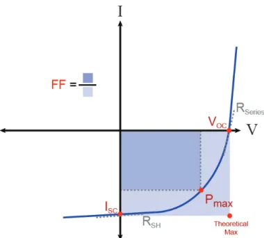
be passed to an external circuit to perform work. When analyzing photovolatic performance, there are
several factors to consider. The first is the short circuit current (
I
SC). This value reflects the maximum
current that can be extracted without an external bias. This value is primarily governed by the physical
size, absorptivity, and charge carrier collection probability of the device. To account for the physical size,
this value is often expressed as a short circuit current density (
J
SC, in mA/cm
2). The second is the open
circuit voltage (
V
OC), or the maximum voltage that the cell can produce. The
V
OCis largely determined
by the magnitude of recombination within the device and the band gap of the material. The third primary
value by which solar cells are characterized is the fill factor (FF). This is the ratio of the maximum power
that the device can produce (
P
max) to the product of the (
I
SC) and (
V
OC), reflecting the overall quality
of the device, and factors into cell efficiency. The ideal diode conforms to the equation
1I
=
I
o(e
qVkB T
−
1)
−
I
L(1.2)
where
I
Lis the photogenerated current and
I
ois the dark saturation current, reflecting the number of
thermally generated charge carriers. However, real devices deviate from ideal behavior. Several additional
factors can be implemented to reflect this behavior in the modified diode equation:
I
=
I
0(e
q(V+IRSeries)
nkB T