In Praise of
Digital Design: An Embedded
Systems Approach Using Verilog
“Peter Ashenden is leading the way towards a new curriculum for educating the next generation of digital logic designers. Recognizing that digital design has moved from being gate-centric assembly of custom logic to processor-centric design of embedded systems, Dr. Ashenden has shifted the focus from the gate to the modern design and integration of complex integrated devices that may be physically realized in a variety of forms. Dr. Ashenden does not ignore the fundamentals, but treats them with suitable depth and breadth to provide a basis for the higher-level material. As is the norm in all of Dr. Ashenden’s writing, the text is lucid and a pleasure to read. The book is illustrated with copious examples and the companion Web site offers all that one would expect in a text of such high quality.”
— g r a n t m a r t i n , Chief Scientist, Tensilica Inc.
“Dr. Ashenden has written a textbook that enables students to obtain a much broader and more valuable understanding of modern digital system design. Readers can be sure that the practices described in this book will provide a strong foundation for modern digital system design using hard-ware description languages.”
— g a r y s p i v e y, George Fox University
“The convergence of miniaturized, sophisticated electronics into handheld, low-power embedded systems such as cell phones, PDAs, and MP3 players depends on efficient, digital design flows. Starting with an intuitive explo-ration of the basic building blocks, Digital Design: An Embedded Systems Approach introduces digital systems design in the context of embedded systems to provide students with broader perspectives. Throughout the text, Peter Ashenden’s practical approach engages students in understand-ing the challenges and complexities involved in implementunderstand-ing embedded systems.”
— g r e g o r y d . p e t e r s o n , University of Tennessee
“Digital Design: An Embedded Systems Approach places emphasis on larger systems containing processors, memory, and involving the design
and interface of I/O functions and application-specific accelerators. The book’s presentation is based on a contemporary view that reflects the real-world digital system design practice. At a time when the university curriculum is generally lagging significantly behind industry development, this book provides much needed information to students in the areas of computer engineering, electrical engineering and computer science.”
— d o n a l d h u n g , San Jose State University
“Digital Design: An Embedded Systems Approach presents the design flow of circuits and systems in a way that is both accessible and up-to-date. Because the use of hardware description languages is state-of-the-art, it is necessary that students learn how to use these languages along with an appropriate methodology. This book presents a modern approach for designing embedded systems starting with the fundamentals and progress-ing up to a complete system—it is application driven and full of many examples. I will recommend this book to my students.”
— g o e r a n h e r r m a n n , TU Chemnitz
“Digital Design: An Embedded Systems Approach is surprisingly easy to read despite the complexity of the material. It takes the reader in a journey from the basics to a real understanding of digital design by answering the ‘whys’ and ‘hows’—it is persuasive and instructive as it moves deeper and deeper into the material.”
— a n d r e y k o p t y u g , Mid Sweden University
“This up-to-date text on digital design is written in a very accessible style using a modern design methodology and the real world of embedded systems as its contexts. Digital Design: An Embedded Systems Approach provides excellent coverage of all aspects of the design of embedded sys-tems, with chapters not just on logic design itself, but also on processors, memories, input/output interfacing and implementation technologies. It’s particularly good at emphasizing the need to consider more than just logic design when designing a digital system: the design has to be implemented in the real world of engineering, where a whole variety of constraints, such as circuit area, circuit interconnections, interfacing requirements, power and performance, must be considered. For those who think logic design is mundane, this book brings the subject to life.”
Digital Design
An Embedded Systems Approach
Using Verilog
a b o u t t h e a u t h o r
Peter J. Ashenden is an Adjunct Associate Professor at Adelaide University and the founder of Ashenden Designs, a consulting business specializing in electronics design automation (EDA).
From 1990 to 2000, Dr. Ashenden was a member of the faculty in the Department of Computer Science at Adelaide. He developed curriculum and taught in a number of areas for both the Computer Sci-ence and the Electrical and Electronic Engineering departments. Topics included computer organization, computer architecture, digital logic design, programming and algorithms, at all levels from undergraduate to graduate courses. He was also actively involved in academic administra-tion at many levels within the university.
In 2000, Dr. Ashenden established Ashenden Designs. His services include training development and delivery, advising on design methodology, research in EDA tool technology, development of design languages, and standards writing. His clients include industry and government organiza-tion in the United States, Europe and SE Asia.
Since 1992, Dr. Ashenden has been involved in the IEEE VHDL standards committees, and continues to play a major role in ongoing development of the language. From 2003 to 2005 he was Chair of the IEEE Design Automation Standards Committee, which oversees development of all IEEE standards in EDA. He is currently Technical Editor for the VHDL, VHDL-AMS, and Rosetta specification language standards.
In addition to his research publications, Dr. Ashenden is author of The Designer’s Guide to VHDL and The Student’s Guide to VHDL, and coauthor of The System Designer’s Guide to VHSL-AMS and VHDL-2007: Just the New Stuff. His VHDL books are highly regarded and are the best-selling references on the subject. From 2000 to 2004, he was Series Coeditor of the Morgan Kaufmann Series on Systems on Silicon, and from 2001 to 2004 he was a member of the Editorial Board ofIEEE Design and Test of Computers magazine.
Dr. Ashenden is a Senior Member of the IEEE and the IEEE Computer Society. He is also a volunteer Senior Firefighter of 12 years standing with the South Australian Country Fire Service.
Digital Design
An Embedded Systems Approach
Using Verilog
p e t e r j . a s h e n d e n
Adjunct Associate Professor School of Computer Science University of Adelaide
amsterdam • boston •heidelberg•london new york •oxford •paris • san diego san francisco • singapore • sydney • tokyo
Publishing Director Joanne Tracy
Publisher Denise E. M. Penrose
Acquisitions Editor Charles Glaser
Publishing Services Manager George Morrison
Senior Production Editor Dawnmarie Simpson
Developmental Editor Nate McFadden
Editorial Assistant Kimberlee Honjo
Production Assistant Lianne Hong
Cover Design Eric DeCicco
Cover Image Corbis
Composition diacriTech
Technical Illustration Peter Ashenden
Copyeditor JC Publishing
Proofreader Janet Cocker
Indexer Joan Green
Interior printer Sheridan Books, Inc.
Cover printer Phoenix Color, Inc. Morgan Kaufmann Publishers is an imprint of Elsevier. 30 Corporate Drive, Suite 400, Burlington, MA 01803, USA This book is printed on acid-free paper.
© 2008 by Elsevier Inc. All rights reserved.
Designations used by companies to distinguish their products are often claimed as trademarks or registered trademarks. In all instances in which Morgan Kaufmann Publishers is aware of a claim, the product names appear in initial capital or all capital letters. Readers, however, should contact the appropriate companies for more complete information regarding trademarks and registration. No part of this publication may be reproduced, stored in a retrieval system, or transmitted in any form or by any means—electronic, mechanical, photocopying, scanning, or otherwise—without prior written permission of the publisher.
Permissions may be sought directly from Elsevier’s Science & Technology Rights Department in Oxford, UK: phone: (+44) 1865 843830, fax: (+44) 1865 853333, E-mail: [email protected]. You may also complete your request online via the Elsevier homepage (http://elsevier.com), by selecting “Support & Contact” then “Copyright and Permission” and then “Obtaining Permissions.”
Library of Congress Cataloging-in-Publication Data Ashenden, Peter J.
Digital design: an embedded systems approach using Verilog / Peter J. Ashenden. p. cm.
Includes index.
ISBN 978-0-12-369527-7 (pbk. : alk. paper) 1. Embedded computer systems. 2. Verilog (Computer hardware description language) 3. System design. I. Title.
TK7895.E42.A68 2007 621.39'16–dc22
2007023242 ISBN: 978-0-12-369527-7
For information on all Morgan Kaufmann publications, visit our Web site at www.mkp.com or www.books.elsevier.com
Printed in the United States. 07 08 09 10 5 4 3 2 1
Working together to grow
libraries in developing countries
www.elsevier.com | www.bookaid.org | www.sabre.orgTo my daughter, Eleanor —pa
ix
c o n t e n t s
Preface . . . xv
c h a p t e r 1 Introduction and Methodology . . . 1
1.1 Digital Systems and Embedded Systems . . . 1
1.2 Binary Representation and Circuit Elements . . . 4
1.3 Real-World Circuits . . . 9
1.3.1 Integrated Circuits . . . 10
1.3.2 Logic Levels . . . 11
1.3.3 Static Load Levels . . . 13
1.3.4 Capacitive Load and Propagation Delay . . . 15
1.3.5 Wire Delay . . . 17
1.3.6 Sequential Timing . . . 17
1.3.7 Power . . . 18
1.3.8 Area and Packaging . . . 19
1.4 Models . . . 21
1.5 Design Methodology . . . 26
1.5.1 Embedded Systems Design . . . 31
1.6 Chapter Summary . . . 33
1.7 Further Reading . . . 34
Exercises . . . 35
c h a p t e r 2 Combinational Basics . . . 39
2.1 Boolean Functions and Boolean Algebra . . . 39
2.1.1 Boolean Functions . . . 39
2.1.2 Boolean Algebra . . . 48
2.1.3 Verilog Models of Boolean Equations . . . 51
2.2 Binary Coding . . . 54
2.2.1 Using Vectors for Binary Codes . . . 56
2.2.2 Bit Errors . . . 58
2.3 Combinational Components and Circuits . . . 62
2.3.1 Decoders and Encoders . . . 62
2.3.2 Multiplexers . . . 68
2.3.3 Active-Low Logic . . . 71
2.4 Verification of Combinational Circuits . . . 74
2.6 Further Reading . . . 82
Exercises . . . 83
c h a p t e r 3 Numeric Basics . . . 87
3.1 Unsigned Integers . . . 87
3.1.1 Coding Unsigned Integers . . . 87
3.1.2 Operations on Unsigned Integers . . . 92
3.1.3 Gray Codes . . . 116
3.2 Signed Integers . . . 119
3.2.1 Coding Signed Integers . . . 119
3.2.2 Operations on Signed Integers . . . 122
3.3 Fixed-Point Numbers . . . 131
3.3.1 Coding Fixed-Point Numbers . . . 131
3.3.2 Operations on Fixed-Point Numbers . . . 136
3.4 Floating-Point Numbers . . . 138
3.4.1 Coding Floating-Point Numbers . . . 138
3.5 Chapter Summary . . . 143
3.6 Further Reading . . . 144
Exercises . . . 144
c h a p t e r 4 Sequential Basics . . . 151
4.1 Storage Elements . . . 151
4.1.1 Flip-flops and Registers . . . 151
4.1.2 Shift Registers . . . 161
4.1.3 Latches . . . 162
4.2 Counters . . . 167
4.3 Sequential Datapaths and Control . . . 175
4.3.1 Finite-State Machines . . . 179
4.4 Clocked Synchronous Timing Methodology . . . 187
4.4.1 Asynchronous Inputs . . . 192
4.4.2 Verification of Sequential Circuits . . . 196
4.4.3 Asynchronous Timing Methodologies . . . 200
4.5 Chapter Summary . . . 203
4.6 Further Reading . . . 204
Exercises . . . 205
c h a p t e r 5 Memories . . . 211
5.1 General Concepts . . . 211
5.2 Memory Types . . . 219
5.2.1 Asynchronous Static RAM . . . 220
5.2.2 Synchronous Static RAM . . . 222
5.2.3 Multiport Memories . . . 229
5.2.4 Dynamic RAM . . . 233
5.2.5 Read-Only Memories . . . 235
5.3 Error Detection and Correction . . . 240
5.4 Chapter Summary . . . 244
5.5 Further Reading . . . 245
Exercises . . . 246
c h a p t e r 6 Implementation Fabrics . . . 249
6.1 Integrated Circuits . . . 249
6.1.1 Integrated Circuit Manufacture . . . 250
6.1.2 SSI and MSI Logic Families . . . 252
6.1.3 Application-Specific Integrated Circuits (ASICs) . . . 255
6.2 Programmable Logic Devices . . . 258
6.2.1 Programmable Array Logic . . . 258
6.2.2 Complex PLDs . . . 262
6.2.3 Field-Programmable Gate Arrays . . . 263
6.3 Packaging and Circuit Boards . . . 269
6.4 Interconnection and Signal Integrity . . . 272
6.4.1 Differential Signaling . . . 276
6.5 Chapter Summary . . . 278
6.6 Further Reading . . . 279
Exercises . . . 280
c h a p t e r 7 Processor Basics . . . 281
7.1 Embedded Computer Organization . . . 281
7.1.1 Microcontrollers and Processor Cores . . . 283
7.2 Instructions and Data . . . 285
7.2.1 The Gumnut Instruction Set . . . 287
7.2.2 The Gumnut Assembler . . . 296
7.2.3 Instruction Encoding . . . 298
7.2.4 Other CPU Instruction Sets . . . 300
7.3 Interfacing with Memory . . . 302
7.3.1 Cache Memory . . . 307
7.4 Chapter Summary . . . 311
7.5 Further Reading . . . 311
Exercises . . . 312
c h a p t e r 8 I/O Interfacing . . . 315
8.1 I/O Devices . . . 315
8.1.1 Input Devices . . . 316
8.1.2 Output Devices . . . 321
8.2 I/O Controllers . . . 330
8.2.1 Simple I/O Controllers . . . 331
8.2.2 Autonomous I/O Controllers . . . 335
8.3 Parallel Buses . . . 338
8.3.1 Multiplexed Buses . . . 338
8.3.2 Tristate Buses . . . 342
8.3.3 Open-Drain Buses . . . 348
8.3.4 Bus Protocols . . . 349
8.4 Serial Transmission . . . 353
8.4.1 Serial Transmission Techniques . . . 353
8.4.2 Serial Interface Standards . . . 357
8.5 I/O Software . . . 360
8.5.1 Polling . . . 360
8.5.2 Interrupts . . . 362
8.5.3 Timers . . . 366
8.6 Chapter Summary . . . 373
8.7 Further Reading . . . 374
Exercises . . . 375
c h a p t e r 9 Accelerators . . . 379
9.1 General Concepts . . . 379
9.2 Case Study: Video Edge-Detection . . . 386
9.3 Verifying an Accelerator . . . 407
9.4 Chapter Summary . . . 419
9.5 Further Reading . . . 419
Exercises . . . 420
c h a p t e r 1 0 Design Methodology . . . 423
10.1 Design Flow . . . 423
10.1.1 Architecture Exploration . . . 425
10.1.2 Functional Design . . . 427
10.1.3 Functional Verification . . . 429
10.1.4 Synthesis . . . 435
10.1.5 Physical Design . . . 438
10.2 Design Optimization . . . 441
10.2.1 Area Optimization . . . 442
10.2.2 Timing Optimization . . . 443
10.2.3 Power Optimization . . . 448
10.3 Design for Test . . . 451
10.3.1 Fault Models and Fault Simulation . . . 452
10.3.2 Scan Design and Boundary Scan . . . 454
10.3.3 Built-In Self Test (BIST) . . . 458
10.4 Nontechnical Issues . . . 462
10.5 In Conclusion . . . 463
10.6 Chapter Summary . . . 465
10.7 Further Reading . . . 466
a p p e n d i x a Knowledge Test Quiz Answers . . . 469
a p p e n d i x b Introduction to Electronic Circuits . . . 501
B.1 Components . . . 501
B.1.1 Voltage Sources . . . 502
B.1.2 Resistors . . . 502
B.1.3 Capacitors . . . 503
B.1.4 Inductors . . . 503
B.1.5 MOSFETs . . . 504
B.1.6 Diodes . . . 506
B.1.7 Bipolar Transistors . . . 507
B.2 Circuits . . . 508
B.2.1 Kirchhoff’s Laws . . . 508
B.2.2 Series and Parallel R, C, and L . . . 509
B.2.3 RC Circuits . . . 511
B.2.4 RLC Circuits . . . 512
B.3 Further Reading . . . 515
a p p e n d i x c Verilog for Synthesis . . . 517
C.1 Data Types and Operations . . . 517
C.2 Combinational Functions . . . 518
C.3 Sequential Circuits . . . 522
C.3.1 Finite-State Machines . . . 525
C.4 Memories . . . 527
a p p e n d i x d The Gumnut Microcontroller Core . . . 531
D.1 The Gumnut Instruction Set . . . 531
D.1.1 Arithmetic and Logical Instructions . . . 531
D.1.2 Shift Instructions . . . 535
D.1.3 Memory and I/O Instructions . . . 536
D.1.4 Branch Instructions . . . 537
D.1.5 Jump Instructions . . . 537
D.1.6 Miscellaneous Instructions . . . 538
D.2 The Gumnut Bus Interface . . . 538
Index . . . 541
p r e f a c e
A P P R O A C H
This book provides a foundation in digital design for students in computer engineering, electrical engineering and computer science courses. It deals with digital design as an activity in a larger systems design context. Instead of focusing on gate-level design and aspects of digital design that have diminishing relevance in a real-world design context, the book concen-trates on modern and evolving knowledge and design skills.
Most modern digital design practice involves design of embedded systems, using small microcontrollers, larger CPUs/DSPs, or hard or soft processor cores. Designs involve interfacing the processor or processors to memory, I/O devices and communications interfaces, and developing accelerators for operations that are too computationally intensive for pro-cessors. Target technologies include ASICs, FPGAs, PLDs and PCBs. This is a significant change from earlier design styles, which involved use of small-scale integrated (SSI) and medium-scale integrated (MSI) circuits. In such systems, the primary design goal was to minimize gate count or IC package count. Since processors had lower performance and memories had limited capacity, a greater proportion of system functionality was implemented in hardware.
While design practices and the design context have evolved, many text-books have not kept track. They continue to promote practices that are largely obsolete or that have been subsumed into computer-aided design (CAD) tools. They neglect many of the important considerations for mod-ern designers. This book addresses the shortfall by taking an approach that embodies modern design practice. The book presents the view that digital logic is a basic abstraction over analog electronic circuits. Like any abstrac-tion, the digital abstraction relies on assumptions being met and constraints being satisfied. Thus, the book includes discussion of the electrical and tim-ing properties of circuits, leadtim-ing to an understandtim-ing of how they influence design at higher levels of abstraction. Also, the book teaches a methodology based on using abstraction to manage complexity, along with principles and methods for making design trade-offs. These intellectual tools allow students to track evolving design practice after they graduate.
Perhaps the most noticeable difference between this book and its predecessors is the omission of material on Karnaugh maps and related
logic optimization techniques. Some reviewers of the manuscript argued that such techniques are still of value and are a necessary foundation for students learning digital design. Certainly, it is important for students to understand that a given function can be implemented by a variety of equivalent circuits, and that different implementations may be more or less optimal under different constraints. This book takes the approach of presenting Boolean algebra as the foundation for gate-level circuit trans-formation, but leaves the details of algorithms for optimization to CAD tools. The complexity of modern systems makes it more important to raise the level of abstraction at which we work and to introduce embed-ded systems early in the curriculum. CAD tools perform a much better job of gate-level optimization than we can do manually, using advanced algorithms to satisfy relevant constraints. Techniques such as Karnaugh maps do have a place, for example, in design of specialized hazard-free logic circuits. Thus, students can defer learning about Karnaugh maps until an advanced course in VLSI, or indeed, until they encounter the need in industrial practice. A web search will reveal many sources describing the techniques in detail, including an excellent article in Wikipedia.
The approach taken in this book makes it relevant to Computer Sci-ence courses, as well as to Computer Engineering and Electrical Engi-neering courses. By treating digital design as part of embedded systems design, the book will provide the understanding of hardware needed for computer science students to analyze and design systems comprising both hardware and software components. The principles of abstraction and complexity management using abstraction presented in the book are the same as those underlying much of computer science and software engineering.
Modern digital design practice relies heavily on models expressed in hardware description languages (HDLs), such as Verilog and VHDL. HDL models are used for design entry at the abstract behavioral level and for refinements at the register transfer level. Synthesis tools produce gate-level HDL models for low-level verification. Designers also express verification environments in HDLs. This book emphasizes HDL-based design and verification at all levels of abstraction. The present version uses Verilog for this purpose. A second version, Digital Design: An Embedded Systems Approach Using VHDL, substitutes VHDL for the same purpose.
OVE RVI EW
For those who are musically inclined, the organization of this book can be likened to a two-act opera, complete with overture, intermezzo, and finale.
Chapter 1 forms the overture, introducing the themes that are to fol-low in the rest of the work. It starts with a discussion of the basic ideas of the digital abstraction, and introduces the basic digital circuit elements.
It then shows how various non-ideal behaviors of the elements impose constraints on what we can design. The chapter finishes with a discussion of a systematic process of design, based on models expressed in a hard-ware description language.
Act I of the opera comprises Chapters 2 through 5. In this act, we develop the themes of basic digital design in more detail.
Chapter 2 focuses on combinational circuits, starting with Boolean algebra as the theoretical underpinning and moving on to binary coding of information. The chapter then surveys a range of components that can be used as building blocks in larger combinational circuits, before return-ing to the design methodology to discuss verification of combinational circuits.
Chapter 3 expands in some detail on combinational circuits used to process numeric information. It examines various binary codes for unsigned integers, signed integers, fixed-point fractions and floating-point real numbers. For each kind of code, the chapter describes how some arithmetic operations can be performed and looks at combinational cir-cuits that implement arithmetic operations.
Chapter 4 introduces a central theme of digital design, sequential cir-cuits. The chapter examines several sequential circuit elements for storing information and for counting events. It then describes the concepts of a datapath and a control section, followed by a description of the clocked synchronous timing methodology.
Chapter 5 completes Act I, describing the use of memories for storing information. It starts by introducing the general concepts that are com-mon to all kinds of semiconductor memory, and then focuses on the par-ticular features of each type, including SRAM, DRAM, ROM and flash memories. The chapter finishes with a discussion of techniques for dealing with errors in the stored data.
The intermezzo, Chapter 6, is a digression away from functional design into physical design and the implementation fabrics used for digi-tal systems. The chapter describes the range of integrated circuits that are used for digital systems, including ASICSs, FPGAs and other PLDs. The chapter also discusses some of the physical and electrical characteristics of implementation fabrics that give rise to constraints on designs.
Act II of the opera, comprising Chapters 7 through 9, develops the embedded systems theme.
Chapter 7 introduces the kinds of processors that are used in ded systems and gives examples of the instructions that make up embed-ded software programs. The chapter also describes the way instructions and data are encoded in binary and stored in memory and examines ways of connecting the processor with memory components.
Chapter 8 expands on the notion of input/output (I/O) controllers that connect an embedded computer system with devices that sense and
affect real-world physical properties. It describes a range of devices that are used in embedded computers and shows how they are accessed by an embedded processor and by embedded software.
Chapter 9 describes accelerators, that is, components that can be added to embedded systems to perform operations faster than is possible with embedded software running on a processor core. This chapter uses an extended example to illustrate design considerations for accelerators, and shows how an accelerator interacts with an embedded processor.
The finale, Chapter 10, is a coda that returns to the theme of design methodology introduced in Chapter 1. The chapter describes details of the design flow and discusses how aspects of the design can be optimized to better meet constraints. It also introduces the concept of design for test, and outlines some design for test tools and techniques. The opera finishes with a discussion of the larger context in which digital systems are designed.
After a performance of an opera, there is always a lively discussion in the foyer. This book contains a number of appendices that correspond to that aspect of the opera. Appendix A provides sample answers for the Knowledge Test Quiz sections in the main chapters. Appendix B provides a quick refresher on electronic circuits. Appendix C is a summary of the subset of Verilog used for synthesis of digital circuits. Finally, Appendix D is an instruction-set reference for the Gumnut embedded processor core used in examples in Chapters 7 through 9.
For those not inclined toward classical music, I apologize if the pre-ceding is not a helpful analogy. An analogy with the courses of a feast came to mind, but potential confusion among readers in different parts of the world over the terms appetizer, entrée and main course make the analogy problematic. The gastronomically inclined reader should feel free to find the correspondence in accordance with local custom.
COU RSE ORGAN I ZATION
This book covers the topics included in the Digital Logic knowledge area of the Computer Engineering Body of Knowledge described in the IEEE/ACM Curriculum Guidelines for Undergraduate Degree Programs in Computer Engineering. The book is appropriate for a course at the sophomore level, assuming only previous introductory courses in electronic circuits and com-puter programming. It articulates into junior and senior courses in embed-ded systems, computer organization, VLSI and other advanced topics.
For a full sequence in digital design, the chapters of the book can be covered in order. Alternatively, a shorter sequence could draw on Chapter 1 through Chapter 6 plus Chapter 10. Such a sequence would defer material in Chapters 7 through 9 to a subsequent course on embedded systems design.
For either sequence, the material in this book should be supplemented by a reference book on the Verilog language. The course work should also include laboratory projects, since hands-on design is the best way to reinforce the principles presented in the book.
WE B SU PPLE M E NTS
No textbook can be complete nowadays without supplementary material on a website. For this book, resources for students and instructors are available at the website:
textbooks.elsevier.com/9780123695277 For students, the website contains:
Source code for all of the example HDL models in the book
Tutorials on the VHDL and Verilog hardware description languages An assembler for the Gumnut processor described in Chapter 7 and Appendix D
A link to the ISE WebPack FPGA EDA tool suite from Xilinx
A link to the ModelSim Xilinx Edition III VHDL and Verilog simula-tor from Mensimula-tor Graphics Corporation
A link to an evaluation edition of the Synplify Pro PFGA synthesis tool from Synplicity, Inc. (see inside back cover for more details). Tutorials on use of the EDA tools for design projects
For instructors, the website contains a protected area with additional resources:
An instructor’s manual Suggested lab projects Lecture notes
Figures from the text in JPG and PPT formats
Instructors are invited to contribute additional material for the benefit of their colleagues.
Despite the best efforts of all involved, some errors have no doubt crept through the review and editorial process. A list of detected errors will be available accumulated on the website mentioned above. Should you detect such an error, please check whether it has been previously recorded. If not, I would be grateful for notice by email to
왘 왘 왘
왘 왘
왘
왘
왘 왘 왘 왘
I would also be delighted to hear feedback about the book and supplementary material, including suggestions for improvement.
ACKNOWLE DG M E NTS
This book arose from my long-standing desire to bring a more modern approach to the teaching of digital design. I am deeply grateful to the folks at Morgan Kaufmann Publishers for supporting me in realizing this goal, and for their guidance and advice in shaping the book. Particular thanks go to Denise Penrose, Publisher; Nate McFadden, Developmental Editor and Kim Honjo, Editorial Assistant. Thanks also to Dawnmarie Simpson at Elsevier for meticulous attention to detail and for making the production process go like clockwork.
The manuscript benefited from comprehensive reviews by Dr. A. Bou-ridane, Queen’s University Belfast; Prof. Goeran Herrmann, Chemnitz University of Technology; Prof. Donald Hung, San Jose State Univer-sity; Prof. Roland Ibbett, University of Edinburgh; Dr. Andrey Koptyug, Mid Sweden University; Dr. Grant Martin, Tensilica, Inc.; Dr. Gregory D. Peterson, University of Tennessee; Brian R. Prasky, IBM; Dr. Gary Spivey, George Fox University; Dr. Peixin Zhong, Michigan State Univer-sity; and an anonymous reviewer from Rensselaer Polytechnic Institute. Also, my esteemed colleague Cliff Cummings of Sunburst Design, Inc., provided technical reviews of the Verilog code and related text. To all of these, my sincere thanks for their contributions. The immense improve-ment from my first draft to the final draft is due to their efforts.
The book and the associated teaching materials also benefited from field testing: in alpha form by myself at the University of Adelaide and by Dr. Monte Tull at The University of Oklahoma; and in beta form by James Sterbenz at The University of Kansas. To them and to their stu-dents, thanks for your forbearance with the errors and for your valuable feedback.
1
1
i n t r o d u c t i o n a n d
m e t h o d o l o g y
This first chapter introduces some of the fundamental ideas underlying design of modern digital systems. We cover quite a lot of ground, but at a fairly basic level. The idea is to set the context for more detailed discus-sion in subsequent chapters.
We start by looking at the basic circuit elements from which digital systems are built, and seeing some of the ways in which they can be put together to perform a required function. We also consider some of the nonideal effects that we need to keep in mind, since they impose con-straints on what we can design. We then focus on a systematic process of design, based on models expressed in a hardware description language. Approaching the design process systematically allows us to develop com-plex systems that meet modern application requirements.
1.1
D I G I TA L S Y S T E M S A N D
E M B E D D E D S Y S T E M S
This book is about digital design. Let’s take a moment to explore those two words. Digital refers to electronic circuits that represent informa-tion in a special way, using just two voltage levels. The main rainforma-tionale for doing this is to increase the reliability and accuracy of the circuits, but as we will see, there are numerous other benefits that flow from the digital approach. We also use the term logic to refer to digital circuits. We can think of the two voltage levels as representing truth values, leading us to use rules of logic to analyze digital circuits. This gives us a strong mathematical foundation on which to build. The word design refers to the systematic process of working out how to construct circuits that meet given requirements while satisfying constraints on cost, performance, power consumption, size, weight and other properties. In this book, we focus on the design aspects and build a methodology for designing complex digital systems.
2 C H A P T E R O N E i n t r o d u c t i o n a n d m e t h o d o l o g y
Digital circuits have quite a long and interesting history. They were preceded by mechanical systems, electromechanical systems, and analog electronic systems. Most of these systems were used for numeric com-putations in business and military applications, for example, in ledger calculations and in computing ballistics tables. However, they suffered from numerous disadvantages, including inaccuracy, low speed, and high maintenance.
Early digital circuits, built in the mid-twentieth century, were con-structed with relays. The contacts of a relay are either open, blocking current flow, or closed, allowing current to flow. Current controlled in this manner by one or more relays could then be used to switch other relays. However, even though relay-based systems were more reliable than their predecessors, they still suffered from reliability and performance problems.
The advent of digital circuits based on vacuum tubes and, sub-sequently, transistors led to major improvements in reliability and performance. However, it was the invention of the integrated circuit (IC), in which multiple transistors were fabricated and connected together, that really enabled the “digital revolution.” As manufacturing technol-ogy has developed, the size of transistors and the interconnecting wires has shrunk. This, along with other factors, has led to ICs, containing billions of transistors and performing complex functions, becoming commonplace now.
At this point, you may be wondering how such complex circuits can be designed. In your electronic circuits course, you may have learned how transistors operate, and that their operation is determined by numerous parameters. Given the complexity of designing a small circuit containing a few transistors, how could it be possible to design a large system with billions of transistors?
The key is abstraction. By abstraction, we mean identifying aspects that are important to a task at hand, and hiding details of other aspects. Of course, the other aspects can’t be ignored arbitrarily. Rather, we make assumptions and follow disciplines that allow us to ignore those details while we focus on the aspects of interest. As an example, the digital abstraction involves only allowing two voltage levels in a circuit, with transistors being either turned “on” (that is, fully conducting) or turned “off” (that is, not conducting). One of the assumptions we make in sup-porting this abstraction is that transistors switch on and off virtually instantaneously. One of the design disciplines we follow is to regulate switching to occur within well-defined intervals of time, called “clock periods.” We will see many other assumptions and disciplines as we pro-ceed. The benefit of the digital abstraction is that it allows us to apply much simpler analysis and design procedures, and thus to build much more complex systems.
1.1 Digital Systems and Embedded Systems C H A P T E R O N E 3
The circuits that we will deal with in this book all perform functions that involve manipulating information of various kinds over time. The information might be an audio signal, the position of part of a machine, or the temperature of a substance. The information may change over time, and the way in which it is manipulated may vary with time.
Digital systems are electronic circuits that represent information in discrete form. An example of the kind of information that we might rep-resent is an audio sound. In the real world, a sound is a continuously vary-ing pressure waveform, which we might represent mathematically usvary-ing a continuous function of time. However, representing that function with any significant precision as a continuously varying electrical signal in a circuit is difficult and costly, due to electrical noise and variation in circuit parameters. A digital system, on the other hand, represents the signal as a stream of discrete values sampled at discrete points in time, as shown in Figure 1.1. Each sample represents an approximation to the pressure value at a given instant. The approximations are drawn from a discrete set of values, for example, the set {10.0, 9.9, 9.8, . . . , 0.1, 0.0, 0.1, . . . , 9.9, 10.0}. By limiting the set of values that can be represented, we can encode each value with a unique combination of digital values, each of which is either a low or high voltage. We shall see exactly how we might do that in Chapter 2. Furthermore, by sampling the signal at regular intervals, say, every 50s, the rate and times at which samples arrive and must be processed is predictable.
Discrete representations of information and discrete sequencing in time are fundamental abstractions. Much of this book is about how to choose appropriate representations, how to process information thus rep-resented, how to sequence the processing, and how to ensure that the assumptions supporting the abstractions are maintained.
The majority of digital systems designed and manufactured today are embedded systems, in which much of the processing work is done by one
F I G U R E 1 . 1 A pressure waveform of a sound, continuously varying over time, and the discrete representation of the waveform in a digital system.
4 C H A P T E R O N E i n t r o d u c t i o n a n d m e t h o d o l o g y
or more computers that form part of the system. In fact, the vast majority of computers in use today are in embedded systems, rather than in PCs and other general purpose systems. Early computers were large systems in their own right, and were rarely considered as components of larger systems. However, as technology developed, particularly to the stage of IC technology, it became practical to embed small computers as compo-nents of a circuit and to program them to implement part of the circuit’s functionality. Embedded computers usually do not take the same form as general purpose computers, such as desktop or portable PCs. Instead, an embedded computer consists of a processor core, together with memory components for storing the program and data for the program to run on the processor core, and other components for transferring data between the processor core and the rest of the system.
The programs running on processor cores form the embedded soft-ware of a system. The way in which embedded softsoft-ware is written bears both similarities and differences with software development for general purpose computers. It is a large topic area in its own right and is beyond the scope of this book. Nonetheless, since we are dealing with embedded systems in this book, we need to address embedded software at least at a basic level. We will return to the topic as part of our discussion of interfac-ing with embedded processor cores in Chapters 8 and 9.
Since most digital systems in use today are embedded systems, most digital design practice involves developing the interface circuitry around processor cores and the application-specific circuitry to perform tasks not done by the cores. That is why this book deals specifically with digital design in the context of embedded systems.
1.2
B I N A R Y R E P R E S E N TAT I O N A N D
C I R C U I T E L E M E N T S
The simplest discrete representation that we see in a digital system is called abinary representation. It is a representation of information that can have only two values. Examples of such information include:
whether a switch is open or closed whether a light is on or off
whether a microphone is active or muted
We can think of these as logical conditions: each is either true or false. In order to represent them in a digital circuit, we can assign a high voltage level to represent the value true, and a low voltage level to represent the value false. (This is just a convention, called positive logic, or active-high logic. We could make the reverse assignment, leading to negative logic, or active-low logic, which we will discuss in Chapter 2.) We often use the values 0 and 1 instead of false and true, respectively. 왘
왘 왘
The values 0 and 1 are binary (base 2) digits, or bits, hence the term binary representation.
The circuit shown in Figure 1.2 illustrates the idea of binary representation. The signal labeled switch_pressed represents the state of the switch. When the push-button switch is pressed, the signal has a high voltage, representing the truth of the condition, “the switch is pressed.” When the switch is not pressed, the signal has a low voltage, representing the falsehood of the condition. Since illumination of the lamp is controlled by the switch, we could equally well have labeled the signal lamp_lit, with a high voltage representing the truth of the condition, “the lamp is lit,” and a low voltage representing the falsehood of the condition.
A more complex digital circuit is shown in Figure 1.3. This circuit includes a light sensor with a digital output, dark, that is true (high volt-age) when there is no ambient light, or false (low voltvolt-age) otherwise. The circuit also includes a switch that determines whether the digital signal lamp_enabled is low or high (that is, false or true, respectively). The sym-bol in the middle of the figure represents an AND gate, a digital circuit element whose output is only true (1) if both of its inputs are true (1). The output is false (0) if either input is false (0). Thus, in the circuit, the signal lamp_lit is true if lamp_enabled is true and dark is true, and is false otherwise. Given this behavior, we can apply laws of logic to analyze the circuit. For example, we can determine that if there is ambient light, the lamp will not light, since the logical AND of two conditions yields falsehood when either of the conditions is false.
The AND gate shown in Figure 1.3 is just one of several basic digital logic components. Some others are shown in Figure 1.4. The AND gate, as
F I G U R E 1 . 3 A digital circuit for a night-light that is only lit when the switch is on and the light sensor shows that it is dark.
lamp_enabled
dark
lamp_lit
sensor +V
1.2 Binary Representation and Circuit Elements C H A P T E R O N E 5
switch_pressed +V
F I G U R E 1 . 2 A circuit in which a switch controls a lamp.
6 C H A P T E R O N E i n t r o d u c t i o n a n d m e t h o d o l o g y
we mentioned above, produces a 1 on its output if both inputs are 1, or a 0 on the output if either input is 0. The OR gate produces the “inclusive or” of its inputs. Its output is 1 if either or both of the inputs is 1, or 0 if both inputs are 0. The inverter produces the “negation” of its input. Its output is 1 if the input is 0, or 0 if the input is 1. Finally, the multiplexer selects between the two inputs labeled “0” and “1” based on the value of the “select” input at the bottom of the symbol. If the select input has the value 0, then the output has the same value as that on the “0” input, whereas if the select input has the value 1, then the output has the same value as that on the “1” input.
We can use these logic gates to build digital circuits that implement more complex logic functions.
e x a m p l e 1 . 1 Suppose a factory has two vats, only one of which is used at a time. The liquid in the vat in use needs to be at the right temperature, between 25˚C and 30˚C. Each vat has two temperature sensors indicating whether the temperature is above 25˚C and above 30˚C, respectively. The vats also have low-level sensors. The supervisor needs to be woken up by a buzzer when the temper-ature is too high or too low or the vat level is too low. He has a switch to select which vat is in use. Design a circuit of gates to activate the buzzer as required. s o l u t i o n For the selected vat, the condition for activating the buzzer is “temperature not above 25˚C or temperature above 30˚C, or level low.” This can be implemented with a gate circuit for each vat. The switch can be used to control the select input of a multiplexer to choose between the circuit outputs for the two vats. The output of the multiplexer then activates the buzzer. The complete circuit is shown in Figure 1.5.
AND gate OR gate
inverter multiplexer
0 1
F I G U R E 1 . 4 Basic digital logic gates.
>30°C
low level
buzzer
>25°C >30°C
low level >25°C
0 1
vat 0
vat 1 select vat 1
select vat 0
+V F I G U R E 1 . 5 The vat buzzer
1.2 Binary Representation and Circuit Elements C H A P T E R O N E 7
Circuits such as those considered above are called combinational. This means that the values of the circuit’s outputs at any given time are determined purely by combining the values of the inputs at that time. There is no notion of storage of information, that is, dependence on val-ues at previous times. While combinational circuits are important as parts of larger digital systems, nearly all digital systems are sequential. This means that they do include some form of storage, allowing the values of outputs to be determined by both the current input values and previous input values.
One of the simplest digital circuit elements for storing information is called, somewhat prosaically, a flip-flop. It can “remember” a single bit of information, allowing it to “flip” and “flop” between a stored 0 state and a stored 1 state. The symbol for a D flip-flop is shown in Figure 1.6. It is called a “D” flip-flop because it has a single input, D, representing the value of the data to be stored: “D” for “data.” It also has another input, clk, called the clock input, that indicates when the value of the D input should be stored. The behavior of the D flip-flop is illustrated in the timing diagram in Figure 1.7. A timing diagram is a graph of the values of one or more signals as they change with time. Time extends along the horizontal axis, and the signals of interest are listed on the vertical axis. Figure 1.7 shows the D input of the flip-flop changing at irregular intervals and the clk input changing periodically. A transition of clk from 0 to 1 is called a rising edge of the signal. (Similarly, a transi-tion from 1 to 0 is called a falling edge.) The small triangular marking next to the clk input specifies that the D value is stored only on a rising edge of the clk input. At that time, the Q output changes to reflect the stored value. Any subsequent changes on the D input are ignored until the next rising edge of clk. A circuit element that behaves in this way is called edge-triggered.
While the behavior of a flip-flop does not depend on the clock input being periodic, in nearly all digital systems, there is a single clock signal that synchronizes all of the storage elements in the system. The system is composed of combinational circuits that perform logical functions on the values of signals and flip-flops that store intermediate results. As we
D Q
clk
F I G U R E 1 . 6 A D fl ip-fl op.
F I G U R E 1 . 7 Timing diagram for a D fl ip-fl op.
D 01 clk 01
Q 01
8 C H A P T E R O N E i n t r o d u c t i o n a n d m e t h o d o l o g y
shall see, use of a single periodic synchronizing clock greatly simplifies design of the system. The clock operates at a fixed frequency and divides time into discrete intervals, called clock periods, or clock cycles. Modern digital circuits operate with clock frequencies in the range of tens to hundreds of megahertz (MHz, or millions of cycles per second), with high-performance circuits extending up to several gigahertz (GHz, or billions of cycles per second). Division of time into discrete intervals allows us to deal with time in a more abstract form. This is another example of abstraction at work.
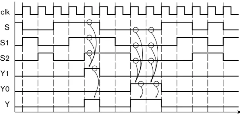
e x a m p l e 1 . 2 Develop a sequential circuit that has a single data input sig-nal, S, and produces an output Y. The output is 1 whenever S has the same value over three successive clock cycles, and 0 otherwise. Assume that the value of S
for a given clock cycle is defi ned at the time of the rising clock edge at the end of the clock cycle.
s o l u t i o n In order to compare the values of S in three successive clock cycles, we need to save the values of S for the previous two cycles and compare them with the current value of S. We can use a pair of D fl ip-fl ops, connected in a pipeline as shown in Figure 1.8, to store the values. When a clock edge occurs, the fi rst fl ip-fl op, ff 1, stores the value of S from the preceding clock cycle. That value is passed onto the second fl ip-fl op, ff 2, so that at the next clock edge, ff 2
stores the value of S from two cycles prior.
The output Y is 1 if and only if three successive value of S are all 1 or are all 0. Gates g1 and g2 jointly determine if the three values are all 1. Inverters g3, g4
and g5 negate the three values, and so gates g6 and g7 determine if the three values are all 0. Gate g8 combines the two alternatives to yield the final output.
D Q
clk
D Q
clk
Y S
clk
ff1
S1
S2
Y1
Y0 ff2
g1
g2
g6
g7
g8
g3
g4
g5 F I G U R E 1 . 8 A sequential
circuit for comparing successive bits of an input.
Figure 1.9 shows a timing diagram of the circuit for a particular sequence of input values on S over several clock cycles. The outputs of the two fl ip-fl ops follow the value of S, but are delayed by one and two clock cycles, respectively. This timing diagram shows the value of S changing at the time of a clock edge. The fl ip-fl op will actually store the value that is on S immediately before the clock edge. The circles and arrows indicate which signals are used to determine the values of other signals, leading to a 1 at the output. When all of S, S1 and S2
are 1, Y1 changes to 1, indicating that S has been 1 for three successive cycles. Similarly, when all of S, S1 and S2 are 0, Y0 changes to 1, indicating that
S has been 0 for three successive cycles. When either of Y1 or Y0 is 1, the output
Y changes to 1.
1. What are the two values used in binary representation?
2. If one input of an AND gate is 0 and the other is 1, what is the output value? What if both are 0, or both are 1?
3. If one input of an OR gate is 0 and the other is 1, what is the output value? What if both are 0, or both are 1?
4. What function is performed by a multiplexer?
5. What is the distinction between combinational and sequential circuits?
6. How much information is stored by a fl ip-fl op?
7. What is meant by the terms rising edge and falling edge?
1.3
R E A L - W O R L D C I R C U I T S
In order to analyze and design circuits as we have discussed, we are making a number of assumptions that underlie the digital abstraction. We have assumed that a circuit behaves in an ideal manner, allowing us to think in
K N O W L E D G E
T E S T Q U I Z
K N O W L E D G E
T E S T Q U I Z
SS1 S2 clk
Y1 Y0 Y
F I G U R E 1 . 9 Timing diagram for the sequential comparison circuit.
10 C H A P T E R O N E i n t r o d u c t i o n a n d m e t h o d o l o g y
terms of 1s and 0s, without being concerned about the circuit’s electrical behavior and physical implementation. Real-world circuits, however, are made of transistors and wires forming part of a physical device or package. The electrical properties of the circuit elements, together with the physical properties of the device or package, impose a number of constraints on circuit design. In this section, we will briefly describe the physical structure of circuit elements and examine some of the most important properties and constraints.
1.3.1 I N T E G R AT E D C I R C U I T S
Modern digital circuits are manufactured on the surface of a small flat piece of pure crystalline silicon, hence the common term “silicon chip.” Such circuits are called integrated circuits, since numerous components are integrated together on the chip, instead of being separate components. We will explore the process by which ICs are manufactured in more detail in Chapter 6. At this stage, however, we can summarize by say-ing that transistors are formed by depositsay-ing layers of semiconductsay-ing and insulating material in rectangular and polygonal shapes on the chip surface. Wires are formed by depositing metal (typically copper) on top of the transistors, separated by insulating layers. Figure 1.10 is a photo-micrograph of a small area of a chip, showing transistors interconnected by wires.
The physical properties of the IC determine many important operat-ing characteristics, includoperat-ing speed of switchoperat-ing between low and high voltages. Among the most significant physical properties is the minimum size of each element, the so-called minimum feature size. Early chips had minimum feature sizes of tens of microns (1 micron1m106m). Improvements in manufacturing technology has led to a steady reduction in feature size, from 10m in the early 1970s, through 1m in the mid 1980s, with today’s ICs having feature sizes of 90nm or 65nm. As well as affecting circuit performance, feature size helps determine the number of transistors that can fit on an IC, and hence the overall circuit complexity. Gordon Moore, one of the pioneers of the digital electronics industry, noted the trend in increasing transistor count, and published an article on the topic in 1965. His projection of a continuing trend continues to this day, and is now known as Moore’s Law. It states that the number of transistors that can be put on an IC for minimum component cost doubles every 18 months. At the time of publication of Moore’s article, it was around 50 transistors; today, a complex IC has well over a billion transistors.
One of the first families of digital logic ICs to gain widespread use was the “transistor-transistor logic” (TTL) family. Components in this family use bipolar junction transistors connected to form logic gates.
F I G U R E 1 . 1 0 Photomicro-graph of a section of an IC.
The electrical properties of these devices led to widely adopted design standards that still influence current logic design practice. In more recent times, TTL components have been largely supplanted by com-ponents using “complementary metal-oxide semiconductor” (CMOS) circuits, which are based on field-effect transistors (FETs). The term “complementary” means that both n-channel and p-channel MOSFETs are used. (See Appendix B for a description of MOSFETS and other circuit components.) Figure 1.11 shows how such transistors are used in a CMOS circuit for an inverter. When the input voltage is low, the n-channel transistor at the bottom is turned off and the p-channel tran-sistor at the top is turned on, pulling the output high. Conversely, when the input voltage is high, the p-channel transistor is turned off and the n-channel transistor is turned on, pulling the output low. Circuits for other logic gates operate similarly, turning combinations of transistors on or off to pull the output low or high, depending on the voltages at the inputs.
1.3.2 L O G I C L E V E L S
The first assumption we have made in the previous discussion is that all signals take on appropriate “low” and “high” voltages, also called logic levels, representing our chosen discrete values 0 and 1. But what should those logic levels be? The answer is in part determined by the characteristics of the electronic circuits. It is also, in part, arbitrary, provided circuit designers and component manufacturers agree. As a consequence, there are now a number of “standards” for logic levels. One of the contributing factors to the early success of the TTL family was its adoption of uniform logic levels for all components in the family. These TTL logic levels still form the basis for standard logic levels in modern circuits.
Suppose we nominate a particular voltage, 1.4V, as our threshold voltage. This means that any voltage lower than 1.4V is treated as a “low” voltage, and any voltage higher than 1.4V is treated as a “high” voltage. In our circuits in preceding figures, we use the ground terminal, 0V, as our low voltage source. For our high voltage source, we used the positive power supply. Provided the supply voltage is above 1.4V, it should be satisfactory. (5V and 3.3V are common power supply voltages for digital systems, with 1.8V and 1.1V also common within ICs.) If components, such as the gates in Figure 1.5, distinguish between low and high volt-ages based on the 1.4V threshold, the circuit should operate correctly. In the real world, however, this approach would lead to problems. Manufac-turing variations make it impossible to ensure that the threshold volt-age is exactly the same for all components. So one gate may drive only slightly higher than 1.4V for a high logic level, and a receiving gate with
output input
+V
F I G U R E 1 . 1 1 CMOS circuit for an inverter.
12 C H A P T E R O N E i n t r o d u c t i o n a n d m e t h o d o l o g y
0.5V 1.0V 1.5V
nominal 1.4V threshold receiver threshold
F I G U R E 1 . 1 2 Problems due to variation in threshold voltage. The receiver would sense the signal as remaining low.
0.5V 1.0V 1.5V 2.0V 2.5V
logic low threshold logic high threshold driven signal
signal with added noise
F I G U R E 1 . 1 3 Problems due to noise on wires.
a threshold a little more above 1.4V would interpret the signal as a low logic level. This is shown in Figure 1.12.
As a way of avoiding this problem, we separate the single thresh-old voltage into two threshthresh-olds. We require that a logic high be greater than 2.0V and a logic low be less than 0.8V. The range in between these levels is not interpreted as a valid logic level. We assume that a signal transitions through this range instantaneously, and we leave the behav-ior of a component with an invalid input level unspecified. However, the signal, being transmitted on an electrical wire, might be subject to external interference and parasitic effects, which would appear as voltage noise. The addition of the noise voltage could cause the signal voltage to enter the illegal range, as shown in Figure 1.13, leading to unspecified behavior.
The final solution is to require components driving digital signals to drive a voltage lower than 0.4V for a “low” logic level and greater than 2.4V for a “high” logic level. That way, there is a noise margin for up to 0.4V of noise to be induced on a signal without affecting its interpretation as a valid logic level. This is shown in Figure 1.14. The symbols for the voltage thresholds are
VOL: output low voltage—a component must drive a signal with a voltage below this threshold for a logic low
VOH: output high voltage—a component must drive a signal with a voltage above this threshold for a logic high
왘
VIL: input low voltage—a component receiving a signal with a voltage below this threshold will interpret it as a logic low VIH: input high voltage—a component receiving a signal with a voltage above this threshold will interpret it as a logic high
The behavior of a component receiving a signal in the region between VIL and VIH is unspecified. Depending on the voltage and other factors, such as temperature and previous circuit operation, the component may interpret the signal as a logic low or a logic high, or it may exhibit some other unusual behavior. Provided we ensure that our circuits don’t violate the assumptions about voltages for logic levels, we can use the digital abstraction.
1.3.3 S TAT I C L O A D L E V E L S
A second assumption we have made is that the current loads on compo-nents are reasonable. For example, in Figure 1.3, the gate output is acting as a source of current to illuminate the lamp. An idealized component should be able to source or sink as much current at the output as its load requires without affecting the logic levels. In reality, component outputs have some internal resistance that limits the current they can source or sink. An idealized view of the internal circuit of a CMOS component’s output stage is shown in Figure 1.15. The output can be pulled high by closing switch SW1 or pulled low by closing switch SW0. When one switch is closed, the other is open, and vice versa. Each switch has a series resistance. (Each switch and its associated resistance is, in practice, a transistor with its on-state series resistance.) When SW1 is closed, current is sourced from the positive supply and flows through R1 to the load con-nected to the output. If too much current flows, the voltage drop across R1 causes the output voltage to fall below VOH. Similarly, when SW0 is closed, the output acts as a current sink from the load, with the current flowing through R0 to the ground terminal. If too much current flows in this direction, the voltage drop across R0 causes the output voltage to rise above VOL. The amount of current that flows in each case depends on the 왘
왘
output R1
SW1 SW0 R0
+V
F I G U R E 1 . 1 5 An idealized view of the output stage of a CMOS component.
1.3 Real-World Circuits C H A P T E R O N E 13
0.5V 1.0V 1.5V 2.0V 2.5V
VIL VOL VIH VOH
driven signal
noise margin signal with added noise
noise margin
F I G U R E 1 . 1 4 Logic level thresholds with noise margin.
14 C H A P T E R O N E i n t r o d u c t i o n a n d m e t h o d o l o g y
output resistances, which are determined by component internal design and manufacture, and the number and characteristics of loads connected to the output. The current due to the loads connected to an output is referred to as the static load on the output. The term static indicates that we are only considering load when signal values are not changing.
The load connected to the AND gate in Figure 1.3 is a lamp, whose current characteristics we can determine from a data sheet or from measurement. A more common scenario is to connect the output of one gate to the inputs of one or more other gates, as in Figure 1.5. Each input draws a small amount of current when the input voltage is low and sources a small amount of current when the input is high. The amounts, again, are determined by component internal design and manufacture. So, as designers using such components and seeking to ensure that we don’t overload outputs, we must ensure that we don’t connect too many inputs to a given output. We use the term fanout to refer to the number of inputs driven by a given output. Manufacturers usually publish current drive and load characteristics of components in data sheets. As a design discipline when designing digital circuits, we should use that information to ensure that we limit the fanout of outputs to meet the static loading constraints.
e x a m p l e 1 . 3 The data sheet for a family of CMOS logic gates that use the TTL logic levels described earlier lists the characteristics shown in Table 1.1. Currents are specifi ed with a positive value for current fl owing into a terminal and a negative value for current fl owing out of a terminal. The
p a r a m e t e r t e s t c o n d i t i o n m i n m a x
VIH 2.0V
VIL 0.8V
IIH 5A
IIL 5A
VOH IOH12mA 2.4V
IOH24mA 2.2V
VOL IOL 12mA 0.4V
IOL 24mA 0.55V
IOH 24mA
IOL 24mA
TA B L E 1 . 1 Electrical characteristics of a family of logic gates.
parameters IIH and IIL are the input currents when the input is at a logic high or low, respectively, and IOH and IOL are the static load currents at an output driving logic high or low, respectively. What is the maximum fanout for an output driving multiple inputs using this logic family, taking account of static loading only?
s o l u t i o n For both high and low logic levels, an output can source or sink up to 24mA of current, and an input load is 5A. Thus each output can drive up to 24mA/5A 4800 inputs. However, in sourcing that much current in the high level, the output voltage may drop to 2.2V, and in the low level, the output voltage may rise to 0.55V. This gives a noise margin of only 0.2V for a high level and 0.15V for a low level. If we want to preserve our 0.4V noise margins, we need to limit the output currents to 12mA, in which case the maximum fanout would be 2400 inputs.
In practice, we cannot connect anywhere near as many inputs to an output as this example might suggest. Static loading is only one factor that determines maximum fanout. In the next part of this section, we will describe another factor that limits fanout more significantly in most designs.
1.3.4 C A PA C I T I V E L O A D A N D P R O PA G AT I O N D E L AY
A further assumption we’ve made in the preceding discussion has been that signals change between logic levels instantaneously. In practice, level changes are not instantaneous, but take an amount of time that depends on several factors that we shall explore. The time taken for the signal voltage to rise from a low level to a high level is called the rise time, denoted by tr, and the time for the signal voltage to fall from a high level to a low level is called the fall time, denoted by tf. These are illustrated in Figure 1.16.
One factor that causes signal changes to occur over a nonzero time interval is the fact that the switches in the output stage of a digital com-ponent, illustrated in Figure 1.15, do not open or close instantaneously. Rather, their resistance changes between near zero and a very large value over some time interval. However, a more significant factor, especially in CMOS circuits, is the fact that logic gates have a significant amount of capacitance at each input. Thus, if we connect the output of one
1.0V 2.0V 3.0V
VOL VOH
tr tf
F I G U R E 1 . 1 6 Rise time and fall time for a signal whose value is changing.
16 C H A P T E R O N E i n t r o d u c t i o n a n d m e t h o d o l o g y
output
input
Cin R1
SW1 SW0 R0
+V
F I G U R E 1 . 17 Connection of an output stage to a capacitively loaded input.
component to the input of another, as shown in Figure 1.17, the input capacitance must be charged and discharged through the output stage’s switch resistances in order to change the logic level on the connecting signal.
If we connect a given output to more than one input, the capacitive loads of the inputs are connected in parallel. The total capacitive load is thus the sum of the individual capacitive loads. The effect is to make transitions on the connecting signal correspondingly slower. For CMOS components, this effect is much more significant than the static load of component inputs. Since we usually want circuits to operate as fast as possible, we are constrained to minimize the fanout of outputs to reduce capacitive loading.
A similar argument regarding time taken to switch transistors on and off and to charge and discharge capacitance also applies within a digital component. Without going into the details of a component’s circuit, we can summarize the argument by saying that, due to the switching time of the internal transistors, it takes some time for a change of logic level at an input to cause a corresponding change at the output. We call that time the propagation delay, denoted by tpd, of the component. Since the time for the output to change depends on the capacitive load, component data sheets that specify propagation delay usually note the capacitive load applied in the test circuit for which the propagation delay was measured, as well as the input capacitance.
e x a m p l e 1 . 4 For a collection of CMOS gate components, the manufacturer’s data sheet specifi es a typical input capacitance, Cin, of 5pF. The AND gate compo-nent has a maximum propagation delay, tpd, of 4.3ns measured with a load capaci-tance, CL, of 50pF. What is the maximum fanout for the AND gate that can be used without causing the propagation delay to exceed the specifi ed maximum?