Discovering the STM32 Microcontroller
Geoffrey Brown ©2012
June 5, 2016
This work is covered by the Creative Commons Attibution-NonCommercial-ShareAlike 3.0 Unported (CC BY-NC-SA 3.0) license.
List of Exercises 7
Foreword 11
1 Getting Started 13
1.1 Required Hardware . . . 16
STM32 VL Discovery . . . 16
Asynchronous Serial . . . 19
SPI . . . 20
I2C . . . 21
Time Based . . . 22
Analog . . . 23
Power Supply . . . 24
Prototyping Materials . . . 25
Test Equipment . . . 25
1.2 Software Installation . . . 26
GNU Tool chain . . . 27
STM32 Firmware Library . . . 27
Code Template . . . 28
GDB Server . . . 29
1.3 Key References . . . 30
2 Introduction to the STM32 F1 31 2.1 Cortex-M3 . . . 34
2.2 STM32 F1 . . . 38
3 Skeleton Program 47 Demo Program . . . 48
Make Scripts . . . 50
CONTENTS
4 STM32 Configuration 57
4.1 Clock Distribution . . . 61
4.2 I/O Pins . . . 63
4.3 Alternative Functions . . . 65
4.4 Remapping . . . 65
4.5 Pin Assignments For Examples and Exercises . . . 66
4.6 Peripheral Configuration . . . 68
5 Asynchronous Serial Communication 71 5.1 STM32 Polling Implementation . . . 76
5.2 Initialization . . . 78
6 SPI 85 6.1 Protocol . . . 85
6.2 STM32 SPI Peripheral . . . 87
6.3 Testing the SPI Interface . . . 90
6.4 EEPROM Interface . . . 92
7 SPI : LCD Display 97 7.1 Color LCD Module . . . 97
7.2 Copyright Information . . . 108
7.3 Initialization Commands (Remainder) . . . 108
8 SD Memory Cards 111 8.1 FatFs Organization . . . 114
8.2 SD Driver . . . 115
8.3 FatFs Copyright . . . 122
9 I2C – Wii Nunchuk 123 9.1 I2C Protocol . . . 124
9.2 Wii Nunchuk . . . 126
9.3 STM32 I2C Interface . . . 131
10 Timers 139 10.1 PWM Output . . . 142
7735 Backlight . . . 142
10.2 Input Capture . . . 146
11 Interrupts 151 11.1 Cortex-M3 Exception Model . . . 155
11.3 NVIC Configuration . . . 159
11.4 Example: Timer Interrupts . . . 160
11.5 Example: Interrupt Driven Serial Communications . . . 161
Interrupt-Safe Queues . . . 165
Hardware Flow Control . . . 167
11.6 External Interrupts . . . 171
12 DMA: Direct Memory Access 179 12.1 STM32 DMA Architecture . . . 181
12.2 SPI DMA Support . . . 182
13 DAC : Digital Analog Converter 189 Warning: . . . 190
13.1 Example DMA Driven DAC . . . 194
14 ADC : Analog Digital Converter 201 14.1 About Successive Approximation ADCs . . . 202
15 NewLib 209 15.1 Hello World . . . 210
15.2 Building newlib . . . 215
16 Real-Time Operating Systems 217 16.1 Threads . . . 219
16.2 FreeRTOS Configuration . . . 224
16.3 Synchronization . . . 225
16.4 Interrupt Handlers . . . 227
16.5 SPI . . . 230
16.6 FatFS . . . 232
16.7 FreeRTOS API . . . 233
16.8 Discusion . . . 234
17 Next Steps 235 17.1 Processors . . . 236
17.2 Sensors . . . 238
Position/Inertial Measurement . . . 238
Environmental Sensors . . . 238
Motion and Force Sensors . . . 239
ID – Barcode/RFID . . . 239
Proximity . . . 239
CONTENTS
17.4 Discussion . . . 239
Attributions 242
List of exercises
Exercise 3.1GDB on STM32 . . . 50
Exercise 4.1Blinking Lights . . . 60
Exercise 4.2Blinking Lights with Pushbutton . . . 65
Exercise 4.3Configuration without Standard Peripheral Library . . 68
Exercise 5.1Testing the USB/UART Interface . . . 73
Exercise 5.2Hello World! . . . 80
Exercise 5.3Echo . . . 84
Exercise 6.1SPI Loopback . . . 91
Exercise 6.2Write and Test an EEPROM Module . . . 96
Exercise 7.1Complete Interface Code . . . 101
Exercise 7.2Display Text . . . 102
Exercise 7.3Graphics . . . 103
Exercise 8.1FAT File System . . . 118
Exercise 9.1Reading Wii Nunchuk . . . 130
Exercise 10.1Ramping LED . . . 144
Exercise 10.2Hobby Servo Control . . . 144
Exercise 10.3Ultrasonic Sensor . . . 149
Exercise 11.1Timer Interrupt – Blinking LED . . . 161
Exercise 11.2Interrupt Driven Serial Communciations . . . 170
Exercise 11.3External Interrupt . . . 173
Exercise 12.1SPI DMA module . . . 185
Exercise 12.2Display BMP Images from Fat File System . . . 185
Exercise 13.1Waveform Generator . . . 190
Exercise 13.2Application Software Driven Conversion . . . 191
Exercise 13.3Interrupt Driven Conversion . . . 192
Exercise 13.4Audio Player . . . 195
Exercise 14.1Continuous Sampling . . . 205
Exercise 14.2Timer Driven Conversion . . . 207
CONTENTS
Exercise 15.1Hello World . . . 213
Exercise 16.1RTOS – Blinking Lights . . . 225
Exercise 16.2Multiple Threads . . . 227
Exercise 16.3Multithreaded Queues . . . 228
Exercise 16.4Multithreaded SPI . . . 232
Acknowledgment
I have had a lot of help from various people in the Indiana University School of Informatics in developing these materials. Most notably, Caleb Hess developed the protoboard that we use in our lab, and he, along with Bryce Himebaugh made significant contributions to the development of the various experiments. Tracey Theriault provided many of the photographs.
I am grateful to ST Microelectronics for the many donations that al-lowed us to develop this laboratory. I particularly wish to thank Andrew Dostie who always responded quickly to any request that I made.
Foreword
This book is intended as a hands-on manual for learning how to de-sign systems using the STM32 F1 family of micro-controllers. It was written to support a junior-level computer science course at Indiana University. The focus of this book is on developing code to utilize the various peripherals avail-able in STM32 F1 micro-controllers and in particular the STM32VL Discovery board. Because there are other fine sources of information on the Cortex-M3, which is the core processor for the STM32 F1 micro-controllers, we do not examine this core in detail; an excellent reference is “The Definitive Guide to the ARM CORTEX-M3.” [5]
This book is not exhaustive, but rather provides a single “trail” to learning about programming STM32 micro controller built around a series of laboratory exercises. A key design decision was to utilize readily available off-the-shelf hardware models for all the experiments discussed.
I would be happy to make available to any instructor the other materi-als developed for teaching C335 (Computer Structures) at Indiana University; however, copyright restrictions limit my ability to make them broadly avail-able.
Chapter 1
Getting Started
The last few years has seen a renaissance of hobbyists and inventors building custom electronic devices. These systems utilize off-the-shelf com-ponents and modules whose development has been fueled by a technological explosion of integrated sensors and actuators that incorporate much of the analog electronics which previously presented a barrier to system develop-ment by non-engineers. Micro-controllers with custom firmware provide the glue to bind sophisticated off-the-shelf modules into complex custom systems. This book provides a series of tutorials aimed at teaching the embedded pro-gramming and hardware interfacing skills needed to use the STM32 family of micro-controllers in developing electronic devices. The book is aimed at read-ers with ’C’ programming experience, but no prior experience with embedded systems.
enables programming them all. 1
Unfortunately, power and flexibility are achieved at a cost – software development for the STM32 family can be extremely challenging for the unini-tiated with a vast array of documentation and software libraries to wade through. For example, RM0041, the reference manual for large value-line STM32 F1 devices, is 675 pages and does not even cover the Cortex-M3 pro-cessor core ! Fortunately, it is not necessary to read this book to get started with developing software for the STM32, although it is an important refer-ence. In addition, a beginner is faced with many tool-chain choices. 2 In
contrast, the Arduino platform offers a simple application library and a single tool-chain which is accessible to relatively inexperienced programmers. For many simple systems this offers a quick path to prototype. However, sim-plicity has its own costs – the Arduino software platform isn’t well suited to managing concurrent activities in a complex real-time system and, for soft-ware interacting with external devices, is dependent upon libraries developed outside the Arduino programming model using tools and techniques similar to those required for the STM32. Furthermore, the Arduino platform doesn’t provide debugging capability which severely limits the development of more complex systems. Again, debugging requires breaking outside the confines of the Arduino platform. Finally, the Arduino environment does not support a real-time operating system (RTOS), which is essential when building more complex embedded systems.
For readers with prior ’C’ programming experience, the STM32 family is a far better platform than the Arduino upon which to build micro-controller powered systems if the barriers to entry can be reduced. The objective of this book is to help embedded systems beginners get jump started with program-ming the STM32 family. I do assume basic competence with C programprogram-ming in a Linux environment – readers with no programming experience are better served by starting with a platform like Arduino. I assume familiarity with a text editor; and experience writing, compiling, and debugging C programs. I do not assume significant familiarity with hardware – the small amount of “wiring” required in this book can easily be accomplished by a rank beginner. The projects I describe in this book utilize a small number of
read-1There are currently five families of STM32 MCUs – STM32 F0, STM32 F1, STM32
L1, STM32 F2, and STM32 F4 supported by different, but structurally similar, firmware libraries. While these families share many peripherals, some care is needed when moving projects between these families. [18, 17, 16]
2A tool-chain includes a compiler, assembler, linker, debugger, and various tools for
ily available, inexpensive, off-the-shelf modules. These include the amazing STM32 VL Discovery board (a $10 board that includes both an STM32 F100 processor and a hardware debugger link), a small LCD display, a USB/UART bridge, a Wii Nunchuk, and speaker and microphone modules. With this small set of components we can explore three of the most important hardware interfaces – serial, SPI, and I2C – analog input and output interfaces, and the development of firmware utilizing both interrupts and DMA. All of the required building blocks are readily available through domestic suppliers as well as ebay vendors. I have chosen not to utilize a single, comprehensive, “evaluation board” as is commonly done with tutorials because I hope that the readers of this book will see that this basic collection of components along with the software techniques introduced provides the concepts necessary to adapt many other off-the-self components. Along the way I suggest other such modules and describe how to adapt the techniques introduced in this book to their use.
The development software used in this book is all open-source. Our primary resource is the GNU software development tool-chain including gcc, gas, objcopy, objdump, and the debugger gdb. I do not use an IDE such as eclipse. I find that most IDEs have a high startup cost although they can ultimately streamline the development process for large systems. IDEs also obscure the compilation process in a manner that makes it difficult to determine what is really happening, when my objective here is to lay bare the development process. While the reader is welcome to use an IDE, I offer no guidance on setting one up. One should not assume that open-source means lower quality – many commercial tool-chains for embedded systems utilize GNU software and a significant fraction of commercial software development is accomplished with GNU software. Finally, virtually every embedded processor is supported by the GNU software chain. Learning to use this tool-chain on one processor literally opens wide the doors to embedded software development.
could have helped isolate this problem – I had to have a way to see the hard-ware behavior. Similarly, when developing code to provide flow-control for a serial interface, I found my assumptions about how the specific USB/UART bridge I was communicating with were wrong. It was only through observing the hardware interface that I found this problem.
In this book I introduce a firmware development process that combines traditional software debugging (with GDB), with the use of a low-cost “logic analyzer” to allow the capture of real-time behavior at hardware interfaces.
1.1 Required Hardware
A list of the hardware required for the tutorials in this book is provided in Figure 1.1. The component list is organized by categories corresponding to the various interfaces covered by this book followed by the required pro-totyping materials and test equipment. In the remainder of this section, I describe each of these components and, where some options exist, key prop-erties that must be satisfied. A few of these components require header pins to be soldered on. This is a fairly simple task that can be accomplished with even a very low cost pencil soldering iron. The amount of soldering required is minimal and I recommend borrowing the necessary equipment if possible. There are many soldering tutorials on the web.
The most expensive component required is a logic analyzer. While I use the Saleae Logic it may be too expensive for casual hobbyists ($150).3 An
alternative, OpenBench Logic Sniffer, is considerably cheaper ($50) and prob-ably adequate. My choice was dictated by the needs of a teaching laboratory where equipment takes a terrific beating – the exposed electronics and pins of the Logic Sniffer are too vulnerable for such an environment. An Oscilloscope might be helpful for the audio interfaces, but is far from essential.
STM32 VL Discovery
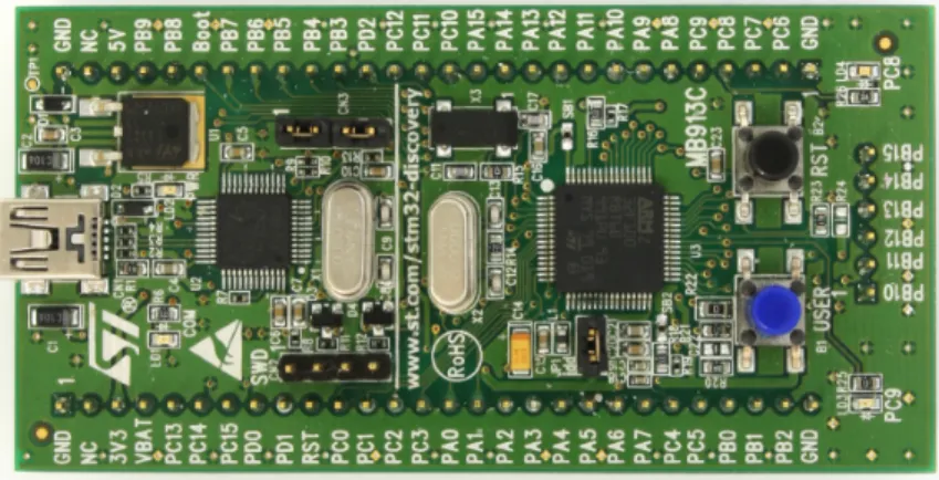
The key component used in the tutorials is the STM32 VL discovery board produced by STMicroelectronics (ST) and available from many electron-ics distributors for approximately $10. 4 This board, illustrated in Figure 1.2
includes a user configurable STM32 F100 micro-controller with 128 KB flash and 8 KB ram as well as an integrated hardware debugger interface based upon a dedicated USB connected STM32 F103. With appropriate software
3At the time of writing Saleae offers a discount to students and professors.
1.1. REQUIRED HARDWARE
Component Supplier cost
Processor
STM32 VL discovery Mouser, Digikey, Future Elec-tronics
$10
Asynchronous Serial
USB/UART breakout Sparkfun, Pololu, ebay $7-$15 SPI
EEPROM (25LC160) Digikey, Mouser, others $0.75
LCD (ST7735) ebay and adafruit $16-$25
Micro SD card (1-2G) Various $5
I2C
Wii Nunchuk ebay (clones), Amazon $6-$12
Nunchuk Adaptor Sparkfun, Adafruit $3
Time Based
Hobby Servo (HS-55 micro) ebay $5
Ultrasonic range finder (HC-SR04) ebay $4
Analog
Potentiometer Digikey, Mouser, ebay $1
Audio amplifier Sparkfun (TPA2005D1) $8
Speaker Sparkfun COM-10722 $1
Microphone Module Sparkfun (BOB-09868 or
BOB-09964)
$8-$10
Power Supply (optional)
Step Down Regulator (2110) Pololu $15
9V Battery Holder 9V Battery
Prototyping Materials
Solderless 700 point breadboard (2) ebay $6
Jumper wires ebay $5-$10
Test Equipment
Saleae Logic or Saleae $150
Oscilloscope optional for testing analog output
Figure 1.1: Required Prototype Hardware and Suppliers
debug-Figure 1.2: STM32 VL Discovery Board
ger interface is accessible through pin headers and can be used to debug any member of the STM32 family – effectively, ST are giving away a hardware debugger interface with a basic prototyping board. The STM32 VL Discovery board is distributed with complete documentation including schematics. [14]. In the photograph, there is a vertical white line slightly to the left of the midpoint. To the right of the line are the STM32 F100, crystal oscillators, two user accessible LEDs, a user accessible push-button and a reset push button. To the left is the hardware debugger interface including an STM32 F103, voltage regulator, and other components. The regulator converts the 5V supplied by the USB connection to 3.3V for the processors and also available at the board edge connectors. This regulator is capable of sourcing sufficient current to support the additional hardware used for the tutorials.
All of the pins of the STM32 F100 are brought out to well labeled headers – as we shall see the pin labels directly correspond to the logical names used throughout the STM32 documentation rather than the physical pins associated with the particular part/package used. This use of logical names is consistent across the family and greatly simplifies the task of designing portable software.
micro-1.1. REQUIRED HARDWARE
controller family.
Asynchronous Serial
One of the most useful techniques for debugging software is to print messages to a terminal. The STM32 micro-controllers provide the necessary capability for serial communications through USART (universal synchronous asynchronous receiver transmitter) devices, but not the physical connection necessary to communicate with a host computer. For the tutorials we utilize a common USB/UART bridge. The most common of these are meant as se-rial port replacements for PCs and are unsuitable for our purposes because they include voltage level converters to satisfy the RS-232 specification. In-stead we require a device which provides more direct access to the pins of the USB/UART bridge device.
Figure 1.3: Pololu CP2102 Breakout Board
An example of such a device, shown in Figure 1.3 is the Pololu cp2102 breakout board. An alternative is the Sparkfun FT232RL breakout board (BOB-00718) which utilizes the FTDI FT232RL bridge chip. I purchased a cp2102 board on ebay which was cheap and works well. While a board with either bridge device will be fine, it is important to note that not all such boards are suitable. The most common cp2102 boards, which have a six pin header, do not provide access the the hardware flow control pins that are essential for reliable high speed connection. An important tutorial in this book covers the implementation of a reliable high-speed serial interface. You should look at the pin-out for any such board to ensure at least the following signals are available – rx, tx, rts, cts.
Figure 1.4: EEPROM in PDIP Package
SPI
The simplest of the two synchronous serial interfaces that we examine in this book is SPI. The key modules we consider are a color LCD display and an SD flash memory card. As these represent relatively complex uses of the SPI interface, we first discuss a simpler device – a serial EEPROM (electrically erasable programmable memory). Many embedded systems use these for persistent storage and it is relatively simple to develop the code necessary to access them.
There are many EEPROMs available with similar, although not iden-tical interfaces. I recommend beginning with the Microchip 25LC160 in a PDIP package (see Figure 1.4). Other packages can be challenging to use in a basic prototyping environment. EEPROMs with different storage densities frequently require slightly different communications protocols.
The second SPI device we consider is a display – we use an inexpen-sive color TFT (thin film transistor) module that includes a micro SD card adaptor slot. While I used the one illustrated in Figure 1.1, an equivalent module is available from Adafruit. The most important constraint is that the examples in this book assume that the display controller is an ST7735 with a SPI interface. We do use the SD card adaptor, although it is possible to find alternative adaptors from Sparkfun and others.
The display is 128x160 pixel full color display similar to those used on devices like ipods and digital cameras. The colors are quite bright and can easily display images with good fidelity. One significant limitation to SPI based displays is communication bandwidth – for high speed graphics it would be advisable to use a display with a parallel interface. Although the value line component on the discovery board does not provide a built-in peripheral to support parallel interfaces, many other STM32 components do.
1.1. REQUIRED HARDWARE
Figure 1.5: Color Display Module
and brand are not critical. The recommended TFT module includes an SD flash memory card slot.
I2C
Figure 1.6: Wii Nunchuk
and two buttons all of which can be polled over the I2C bus. These are widely available in both genuine and clone form. I should note that there appear to be some subtle differences between the various clones that may impact software development. The specific problem is a difference in initialization sequences and data encoding.
Figure 1.7: Wii Nunchuk Adaptor
The connector on the Nunchuk is proprietary to Wii and I have not found a source for the mating connector. There are simple adaptor boards available that work well for the purposes of these tutorials. These are available from several sources; the Sparkfun version is illustrated in Figure 1.7.
Time Based
1.1. REQUIRED HARDWARE
of USB it is desirable to use a “micro” servo for the experiments described in this book.
Figure 1.8: Servo
Figure 1.9: Ultrasonic Sensor
Analog
The final interface that we consider is analog – both in (analog to digital) and out (digital to analog). A digital to analog converter (DAC) translates a digital value into a voltage. To illustrate this capability we use a DAC to drive a small speaker through an amplifier (Figure 1.11). The particular experiment, reading audio files off an SD memory card and playing then through a speaker, requires the use of multiple interfaces as well as timers and DMA.
Figure 1.10: Common Potentiometer
Figure 1.11: Speaker and Amplifier
Figure 1.12: Microphone
Power Supply
1.1. REQUIRED HARDWARE
Figure 1.13: Power Supply
Prototyping Materials Need pictures
In order to provide a platform for wiring the various components to-gether, I recommend purchasing two 700-tie solder less bread boards along with a number of breadboard jumper wires in both fefemale and male-male configuration. All of these are available on ebay at extremely competitive prices.
Test Equipment
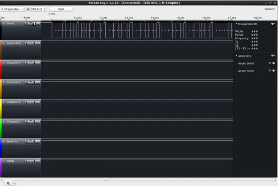
The Saleae Logic logic analyzer is illustrated in Figure 1.14. This device provides a simple 8-channel logic analyzer capable of capturing digital data at 10-20 MHz which is sufficiently fast to debug the basic serial protocols utilized by these tutorials. While the hardware itself is quite simple – even primitive – the software provided is very sophisticated. Most importantly, it has the capability of analyzing several communication protocols and displaying the resulting data in a meaningful manner. Figure 1.15 demonstrates the display of serial data – in this case “hello world” (you may need to zoom in your pdf viewer to see the details).
Figure 1.14: Saleae Logic
Figure 1.15: Saleae Logic Software
1.2 Software Installation
1.2. SOFTWARE INSTALLATION
access to all of the peripherals of the STM32 family. While these libraries are relatively complicated, this book will provide a road map to their use as well some initial shortcuts. The advantages to the using these firmware libraries are that they abstract much of the bit-level detail required to program the STM32, they are relatively mature and have been thoroughly tested, and they enable the development of application code that is portable across the STM32 family. In contrast, we have examined the sample code distributed with the NXP LPC13xx Cortex-M3 processors and found it to be incomplete and in a relatively immature state.
GNU Tool chain
The software development for this book was performed using the GNU embedded development tools including gcc, gas, gdb, and gld. We have suc-cessfully used two different distributions of these tools. In a linux environment we use the Sourcery (a subsidiary of Mentor Graphics) CodeBench Lite Edi-tion for ARM (EABI). These may be obtained athttps://sourcery.mentor.
com/sgpp/lite/arm/portal/subscription?@template=lite. I recommend
using the GNU/Linux installer. The site includes PDF documentation for the GNU tool chain along with a “getting started” document providing detailed installation instructions.
Adding the following to your Linux bash initialization will make access simpler
export PATH=path-to/codesourcery/bin:$PATH
On OS X systems (Macs) we use the yagarto (www.yagarto.de) distri-bution of the GNU toolchain. There is a simple installer available for down-load.
STM32 Firmware Library
The STM32 parts are well supported by a the ST Standard Peripheral Library5 which provides firmware to support all of the peripherals on the var-ious STM32 parts. This library, while easy to install, can be quite challenging to use. There are many separate modules (one for each peripheral) as well as large numbers of definitions and functions for each module. Furthermore, compiling with these modules requires appropriate compiler flags as well as
a few external files (a configuration file, and a small amount of code). The approach taken in this documentation is to provide a basic build environment (makefiles, configuration file, etc.) which can be easily extended as we explore the various peripherals. Rather than attempt to fully describe this peripheral library, I present modules as needed and then only the functions/definitions we require.
Code Template
While the firmware provided by STMicroelectronics provides a solid foundation for software development with the STM32 family, it can be difficult to get started. Unfortunately, the examples distributed with the STM32 VL Discovery board are deeply interwoven with the commercial windows-based IDEs available for STM32 code development and are challenging to extract and use in a Linux environment. I have created a small template example which uses standard Linux make files and in which all aspects of the build process are exposed to the user.
STM32-Template/ BlinkLight.elf Demo/
main.c Makefile Library/
· · ·
Makefile.common README.md
startup_STM32F10x.c STM32F100.ld
STM32F10x_conf.h
Figure 1.16: STM32VL Template
This template can be downloaded as follows:
git clone git://github.com/geoffreymbrown/STM32-Template.git
1.2. SOFTWARE INSTALLATION
header file required by the standard peripheral library. A subdirectory con-tains the code and example specific makefile. The directory includes a working binary for the STM32 VL Discovery. The Demo program is discussed further in Chapter 3.
GDB Server
In order to download and debug code on the STM32 VL Discovery board we can exploit the built-in USB debugger interface called stlink which com-municates with the STM32 on-chip debug module. The stlink interface can be used both for the processor on the Discovery board and, by setting jumper appropriately, for off-board processors. ST also sells a stand-alone version of this debugger interface. Sadly, the stlink interface is only supported on Windows and ST has not publicly released the interface specification. It is widely known that the stlink interface is implemented using the USB Mass Storage device class and it is further known that this particular implementa-tion is incompatible with the OS X and Linux kernel drivers. Nevertheless, the interface has been sufficiently reverse-engineered that a very usable gdb server running on Linux or OS X is available for download:
git clone git://github.com/texane/stlink.git
The README file describes the installation process. The STM32VL Discovery board utilizes the STLINKv1 protocol which is somewhat problem-atic in either case because of the manner in which it interacts with the OS Kernel. Because of the kernel issues, it is important to follow the directions provided. In the case of OS X, there is also a “mac os x driver” which must be built and installed.
To execute the gdb server, plug in an STM32 VL discovery board. Check to see if “/dev/stlink” exists and then execute:
st-util -1
Note: earlier versions of st-util need a different startup sequence
st-util 4242 /dev/stlink
arm-none-eabi-gdb BlinkingLights.elf (gdb) target extended-remote :4242 (gdb) load
(gdb) continue
This will download the program to flash and begin execution. GDB can also be used to set breakpoints and watchpoints.
1.3 Key References
There are an overwhelming number of documents pertaining the the STM32 family of Cortex-M3 MCUs. The following list includes the key docu-ments referred to in this book. Most of these are available on-line from www. st.com. The Cortex-M3 technical reference is available from www.arm.com.
RM0041 Reference manual for STM32F100x Advanced ARM-based 32-bit MCUs [20]. This document provides reference information on all of the peripheral used in the STM32 value line processors including the processor used on the STM32 VL Discovery board.
PM0056 STM32F10xx/20xx/21xx/L1xxx [19]. ST reference for program-ming the Cortex-M3 core. Include the execution model and instruction set, and core peripherals (e.g. the interrupt controller).
Cortex-M3 ARM Cortex-M3 (revision r1p1) Technical Reference Manual. The definitive source for information pertaining to the Cortex-M3 [1].
Data Sheet Low & Medium-density Value Line STM32 data sheet [15]. Pro-vides pin information – especially the mapping between GPIO names and alternative functions. There are data sheets for a number of STM32 family MCUs – this one applies to the MCU on the STM32 VL discovery board.
Chapter 2
Introduction to the STM32
F1
The STM32 F1xx micro-controllers are based upon the ARM Cortex-M3 core. The Cortex-Cortex-M3 is also the basis for micro-controllers from a number of other manufacturers including TI, NXP, Toshiba, and Atmel. Sharing a common core means that the software development tools including com-piler and debugger are common across a wide range of micro-controllers. The Cortex-M3 differs from previous generations of ARM processors by defining a number of key peripherals as part of the core architecture including interrupt controller, system timer, and debug and trace hardware (including external interfaces). This additional level of integration means that system software such as real-time operating systems and hardware development tools such as debugger interfaces can be common across the family of processors. The var-ious Cortex-M3 based micro-controller families differ significantly in terms of hardware peripherals and memory – the STM32 family peripherals are com-pletely different architecturally from the NXP family peripherals even where they have similar functionality. In this chapter we introduce key aspects of the Cortex-M3 core and of the STM32 F1xx micro-controllers.
USART1 SPI1 TIM1 TIM17 TIM16 TIM15 GPIOE GPIOD GPIOC GPIOB GPIOA 12-bit ADC1 EXTIT I2C2 I2C1 HDMI CEC SPI2 USART3 USART2 TIM4 TIM3 TIM2 DAC1 DAC2 WWDG TIM8 TIM7 APB2 APB1 Bus Matrix Cortex-M3 DMA Flash (128KB) SRAM (8KB) AHB2 APB2 AHB1 APB1 STM32F100 (simplified)
Figure 2.1: STM32 F100 Architecture
specific hardware is through three memory buses – ICode, DCode, and System – which are defined to access different regions of memory.
Cortex-M3
Bus
Matrix ICode DCode System NVIC
SysTick
Interrupts CM3 Core
Inst Data
Figure 2.2: Simplified Cortex-M3 Core Architecture
DMA Cortex-M3 Bus Matrix Flash Memory ICode DCode System DMA SRAM Bridge 1 Bridge 2 AHB Bus ADC1 AFIO GPIOx SPI1 TIM1 TIM15 TIM16 TIM17 USART1 APB2 BKP CEC DAC I2C1 I2C2 SPI2 TIM2 TIM3 TIM4 TIM6 TIM7 USART2 USART3 WWDG APB1
Figure 2.3: STM32 Medium Density Value-Line Bus Architecture
2.1 Cortex-M3
The CM3 processor implements the Thumb-2 instruction set which pro-vides a large set of 16-bit instructions, enabling 2 instructions per memory fetch, along with a small set of 32-bit instructions to support more complex operations. The specific details of this instruction set are largely irrelevant for this book as we will be performing all our programming in C. However, there are a few key ideas which we discuss in the following.
2.1. CORTEX-M3
int counter ;
int counterInc (void){ return counter ++; }
The resulting (annotated) assembly language with corresponding ma-chine code follows:
counterInc :
0: f240 0300 movw r3 , #: lower16 : counter // r3 = & counter
4: f2c0 0300 movt r3 , #: upper16 : counter
8: 6818 ldr r0 , [r3 , #0] // r0 = *r3
a: 1c42 adds r2 , r0 , #1 // r2 = r0 + 1
c: 601a str r2 , [r3 , #0] // *r3 = r2
e: 4740 bx lr // return r0
Two 32-bit instructions (movw, movt) are used to load the lower/upper halves of the address of counter (known at link time, and hence 0 in the code listing). Then three 16-bit instructions load (ldr) the value of counter, increment (adds) the value, and write back (str) the updated value. Finally, the procedure returns the original counter.
It is not expected that the reader of this book understand the Cortex-M3 instruction set, or even this example in great detail. The key points are that the Cortex-M3 utilizes a mixture of 32-bit and 16-bit instructions (mostly the latter) and that the core interacts with memory solely through load and store instructions. While there are instructions that load/store groups of registers (in multiple cycles) there are no instructions that directly operate on memory locations.
The Cortex-M3 core has 16 user-visible registers (illustrated in Fig-ure 2.4) – all processing takes place in these registers. Three of these registers have dedicated functions including the program counter (PC), which holds the address of the next instruction to execute, the link register (LR), which holds the address from which the current procedure was called, and “the” stack pointer (SP) which holds the address of the current stack top (as we shall discuss in Chapter 11, the CM3 supports multiple execution modes, each with their own private stack pointer). Separately illustrated is a processor status register (PSR) which is implicitly accessed by many instructions.
r0 r1 r2 r3 r4 r5 r6 r7 r8 r9 r10 r11 r12
r13 (SP) PSP MSP r14 (LR)
r15 (PC)
PSR
Figure 2.4: Processor Register Set
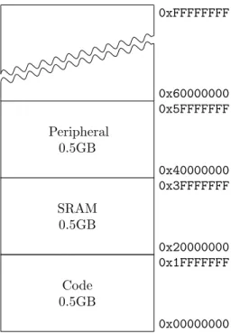
application binary interface) which dictates how registers are used. [2] This model explicitly assumes that the RAM for an executing program is divided into three regions as illustrated in Figure 2.5. The data in RAM are allocated during the link process and initialized by startup code at reset (see Chapter 3). The (optional) heap is managed at runtime by library code implementing func-tions such as the mallocand free which are part of the standard C library. The stack is managed at runtime by compiler generated code which generates per-procedure-call stack frames containing local variables and saved registers. The Cortex-M3 has a “physical” address space of 232 bytes. The ARM
Cortex-M3 Technical Reference Manual defines how this address space is to be used. [1] This is (partially) illustrated in Figure 2.6. As mentioned, the “Code” region is accessed through the ICode (instructions) and DCode (constant data) buses. The SRAM and Peripheral areas are accessed through the System bus. The physical population of these regions is implementation dependent. For example, the STM32 processors have 8K–1M flash memory based at address (0x08000000). 1 The STM32F100 processor on the Discovery board has 8K of SRAM based at address 0x20000000. Not shown on this address map are the internal Cortex-M3 peripherals such as the NVIC which is located starting at
2.1. CORTEX-M3
Data
Heap End Main Stack
SP
RAM Start (low) RAM End (high)
Heap Start
Figure 2.5: Program Memory Model
address 0xE000E000; these are defined in the Cortex-M3 reference manual. [1] We discuss the NVIC further in Chapter 11.
Code 0.5GB
0x00000000 0x1FFFFFFF
SRAM 0.5GB
0x20000000 0x3FFFFFFF
Peripheral 0.5GB
0x40000000 0x5FFFFFFF 0x60000000 0xFFFFFFFF
As mentioned, the Cortex-M3 core includes a vectored interrupt con-troller (NVIC) (see Chapter 11 for more details). The NVIC is a programmable device that sits between the CM3 core and the micro-controller. The Cortex-M3 uses a prioritized vectored interrupt model – the vector table is defined to reside starting at memory location 0. The first 16 entries in this table are de-fined for all Cortex-M3 implementations while the remainder, up to 240, are implementation specific; for example the STM32F100 devices define 60 ad-ditional vectors. The NVIC supports dynamic redefinition of priorities with up to 256 priority levels – the STM32 supports only 16 priority levels. Two entries in the vector table are especially important: address 0 contains the address of the initial stack pointer and address 4 contains the address of the “reset handler” to be executed at boot time.
The NVIC also provides key system control registers including the Sys-tem Timer (SysTick) that provides a regular timer interrupt. Provision for a built-in timer across the Cortex-M3 family has the significant advantage of making operating system code highly portable – all operating systems need at least one core timer for time-slicing. The registers used to control the NVIC are defined to reside at address0xE000E000and are defined by the Cortex-M3 specification. These registers are accessed with the system bus.
2.2 STM32 F1
The STM32 is a family of controllers. The STM32 F1xx micro-controllers are based upon the Cortex-M3 and include the STM32F100 value-line micro-controller used on the discovery board considered in this book. The STM32 L1 series is derived from the STM32 F1 series but with reduced power consumption. The STM32 F2 series is also based upon the Cortex-M3 but has an enhanced set of peripherals and a faster processor core. Many of the peripherals of the STM32 F1 series are forward compatible, but not all. The STM32 F4 series of processors use the Cortex-M4 core which is a significant enhancement of the Cortex-M3. Finally, there is a new STM32 family – the STM32 F0 based upon the Cortex-M0. Each of these families – STM32F0, STM32 F1, STM32 L1. STM32 F2, and STM32 F4 are supported by different firmware libraries. While there is significant overlap between the families and their peripherals, there are also important differences. In this book we focus on the STM32 F1 family.
2.2. STM32 F1
controlled by the core with load and store instructions that access memory-mapped registers. The peripherals can “interrupt” the core to request atten-tion through peripheral specific interrupt requests routed through the NVIC. Finally, data transfers between peripherals and memory can be automated using DMA. In Chapter 4 we discuss basic peripheral configuration, in Chap-ter 11 we show how inChap-terrupts can be used to build effective software, and in Chapter 12 we show how to use DMA to improve performance and allow processing to proceed in parallel with data transfer.
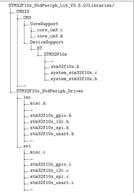
Throughout this book we utilize the ST Standard Peripheral Library for the STM32 F10xx processors. It is helpful to understand the layout of this soft-ware library. Figure 2.7 provides a simplified view of the directory structure. The library consists of two major sub-directories – STM32F10x_StdPeriph_Driver and CMSIS. CMSIS stands for “Cortex Micro-controller Software Interface Standard” and provides the common low-level software required for all ARM Cortex parts. For example, the core_cm3.* files provide access to the inter-rupt controller, the system tick timer, and the debug and trace modules. The STM32F10x_StdPeriph_Driver directory provides roughly one module (23 in all) for each of the peripherals available in the STM32 F10x family. In the figure, I have included modules for general purpose I/O (GPIO), I2C, SPI, and serial IO (USART). Throughout this book I will introduce the modules as necessary.
There are additional directories distributed with the firmware libraries that provide sample code which are not illustrated. The supplied figure pro-vides the paths to all of the key components required to build the tutorials in this book.
The STM32 F1 has a sophisticated clock system. There are two primary external sources of timing – HSE and LSE. The HSE signal is derived from an 8MHz crystal or other resonator, and the LSE signal is derived from a 32.768 kHz crystal. Internally, the HSE is multiplied in frequency through the use of a PLL; the output of this, SYSCLK is used to derive (by division) various on-chip time sources include clocks for the ABP1 and APB2 peripherals as well as for the various programmable timers. The LSE is used to manage a low-power real-time clock. The STM32F100 micro-controllers can support a maximum SYSCLK frequency of 24MHz while the other STM32 F1xx micro-controllers support a SYSCLK frequency of 72MHz. Fortunately, most of the code re-quired to manage these clocks is provided in the standard peripheral library module (system_stm32f10x.[ch]) which provides an initialization function –SystemInit(void)to be called at startup. This module also exports a
STM32F10x_StdPeriph_Lib_V3.5.0/Libraries/ CMSIS
CM3
CoreSupport core_cm3.c core_cm3.h DeviceSupport
ST
STM32F10x …
stm32f10x.h
system_stm32f10x.c system_stm32f10x.h …
STM32F10x_StdPeriph_Driver inc
misc.h …
stm32f10x_gpio.h stm32f10x_i2c.h stm32f10x_spi.h stm32f10x_usart.h …
src misc.c …
stm32f10x_gpio.c stm32f10x_i2c.c stm32f10x_spi.c stm32f10x_usart.c …
Figure 2.7: ST Standard Peripheral Library
the task of developing code that is portable across the STM32F1 family.
2.2. STM32 F1
ADC Analog to digital converter – Chapter 14.
DAC Digital to analog converter – Chapter 13.
GPIO General Purpose I/O – Chapter 4.
I2C I2C bus – Chapter 9.
SPI SPI bus – Chapter 6.
TIM Timers (various) – Chapter 10.
USART Universal synchronous asynchronous receiver transmitter – Chap-ter 5.
The following peripherals are not considered in this book.
CAN Controller area network. Not supported by STM32F100
CEC Consumer electronics control.
CRC Cyclic redundancy check calculation unit.
ETH Ethernet interface. Not supported by the STM32F100
FSMC Flexible static memory controller. Not supported by medium density STMF100.
PWR Power control (sleep and low power mode).
RTC Real time clock.
IWDG Independent watchdog.
USB Universal serial bus. Not supported by the STM32F100
WWDG Windowing watchdog
As mentioned previously all of the peripherals are “memory-mapped” which means that the core interacts with the peripheral hardware by reading and writing peripheral “registers” using load and store instructions. 2 All of
2The terminology can be confusing – from the perspective of the CM3 core, peripheral
the various peripheral registers are documented in the various STM32 refer-ence manuals ([20, 21]). The documentation include bit-level definitions of the various registers and text to help interpret those bits. The actual physical addresses are also found in the reference manuals.
The following table provides the address for a subset of the peripherals that we consider in this book. Notice that all of these fall in the area of the Cortex-M3 address space defined for peripherals.
0x40013800 - 0x40013BFF USART1
0x40013000 - 0x400133FF SPI1
0x40012C00 - 0x40012FFF TIM1 timer
0x40012400 - 0x400127FF ADC1
... ...
Fortunately, it is not necessary for a programmer to look up all these values as they are defined in the library file stm32f10x.h as USART1_BASE,
SPI1_BASE,TIM1_BASE ADC1_BASE, etc.
Typically, each peripheral will have control registers to configure the peripheral, status registers to determine the current peripheral status, and data registers to read data from and write data to the peripheral. Each GPIO port (GPIOA, GPIOB, etc.) has seven registers. Two are used to configure the sixteen port bits individually, two are used to read/write the sixteen port bits in parallel, two are used to set/reset the sixteen port bits individually, and one is used to implement a “locking sequence” that is intended to prevent rogue code from accidentally modifying the port configuration. This final feature can help minimize the possibility that software bugs lead to hardware failures; e.g, accidentally causing a short circuit.
In addition to providing the addresses of the peripherals,stm32f10x.h
also provides C language level structures that can be used to access each peripherals. For example, the GPIO ports are defined by the following register structure.
typedef struct {
2.2. STM32 F1
The register addresses of the various ports are defined in the library as (the following defines are from stm32f10x.h)
# define PERIPH_BASE (( uint32_t )0 x40000000 ) # define APB2PERIPH_BASE ( PERIPH_BASE + 0 x10000 ) # define GPIOA_BASE ( APB2PERIPH_BASE + 0x0800) # define GPIOA (( GPIO_TypeDef *) GPIOA_BASE )
To read the 16 bits of GPIOA in parallel we might use the following code:
uint16_t GPIO_ReadInputData ( GPIO_TypeDef * GPIOx) { return (( uint16_t )GPIOx ->IDR);
}
The preceding example is somewhat misleading in its simplicity. Con-sider that to configure a GPIO pin requires writing two 2-bit fields at the correct location in correct configuration register. In general, the detail re-quired can be excruciating.
Fortunately, the standard peripheral library provides modules for each peripheral that can greatly simplify this task. For example, the following is a subset of the procedures available for managing GPIO ports:
void GPIO_Init ( GPIO_TypeDef * GPIOx ,
GPIO_InitTypeDef * GPIO_InitStruct ); uint8_t GPIO_ReadInputDataBit ( GPIO_TypeDef * GPIOx , uint16_t GPIO_Pin ); uint16_t GPIO_ReadInputData ( GPIO_TypeDef * GPIOx); uint8_t GPIO_ReadOutputDataBit ( GPIO_TypeDef * GPIOx ,
uint16_t GPIO_Pin ); uint16_t GPIO_ReadOutputData ( GPIO_TypeDef * GPIOx );
void GPIO_SetBits ( GPIO_TypeDef * GPIOx , uint16_t GPIO_Pin ); void GPIO_ResetBits ( GPIO_TypeDef * GPIOx , uint16_t GPIO_Pin ); void GPIO_WriteBit ( GPIO_TypeDef * GPIOx , uint16_t GPIO_Pin ,
BitAction BitVal );
void GPIO_Write ( GPIO_TypeDef * GPIOx , uint16_t PortVal );
The initialization function (GPIO_Init) provides an interface for con-figuring individual port bits. The remaining functions provide interfaces for reading and writing (also setting and resetting) both individual bits and the 16 port bits in parallel.
code. Furthermore, the code can be slow – often multiple procedure calls are used by the library where none would be required by custom code. Never-theless, the library offers a much faster path to correct prototype code. For prototype work, it’s probably better to throw extra hardware (memory, clock rate) at a problem than sweat the details. For serious product development it may be wise to refine a design to reduce dependence on these libraries.
To get a sense of the cost of using the library consider the code in Figure 2.1 which configures PC8 and PC9 as outputs (to drive LEDs) and PA0 as an input (to read the push button). 3. Similar library based code
is presented as an exercise in Chapter 4. In Table 2.1 I compare the space requirements of two versions of this program with and without the use of the standard peripheral library. The first column (text) provides the size of “text segment” (code and data initializers), the data allocated in ram at startup is the sum of data (initialized data) and bss (zeroed data). The total memory requirements are provided in column text. The .elf files are the complete binaries. Excluding 256 bytes of preallocated runtime stack (bss), the library version is nearly 3 times as large. Unlike the original which did minimum system initialization, I included two common startup files for both versions. Also, the standard peripheral library has extensive parameter checking which I disabled for this comparison.
Code With Libraries text data bss dec filename
200 0 0 200 main.o
576 0 0 576 startup_stm32f10x.o 832 0 0 832 stm32f10x_gpio.o 1112 20 0 1132 stm32f10x_rcc.o
484 20 0 504 system_stm32f10x.o 3204 40 256 3500 blinky2-lib.elf
Code Without Libraries text data bss dec filename
136 0 0 136 main.o
576 0 0 576 startup_stm32f10x.o 484 20 0 504 system_stm32f10x.o 1196 20 256 1472 blinky2.elf
Table 2.1: Code Size With and Without Standard Libraries
2.2. STM32 F1
# include <stm32f10x .h> int main(void){
int n = 0; int button ;
/* Enable the GPIOA (bit 2) and GPIOC (bit 4) */ /* See 6.3.7 in stm32f100x reference manual */
RCC -> APB2ENR |= 0x10 | 0x04;
/* Set GPIOC Pin 8 and Pin 9 to outputs */ /* 7.2.2 in stm32f100x reference manual */
GPIOC ->CRH = 0x11;
/* Set GPIOA Pin 0 to input floating */ /* 7.2.1 in stm32f100x reference manual */
GPIOA ->CRL = 0x04;
while (1){ delay ();
// Read the button - the button pulls down PA0 to logic 0
button = (( GPIOA ->IDR & 0x1) == 0); n++;
/* see 7.2.5 in stm32f100x reference manual */
if (n & 1) {
GPIOC ->BSRR = 1<<8 ; } else {
GPIOC ->BSRR = 1 < <24; }
if ((n & 4) && button ) { GPIOC ->BSRR = 1<<9 ; } else {
GPIOC ->BSRR = 1 < <25; }
} }
void delay(void){
int i = 100000;/* About 1/4 second delay */
while (i-- > 0) asm("nop"); }
Chapter 3
Skeleton Program
In this chapter I discuss the process of creating, compiling, loading, executing, and debugging a program with the STM32 VL Discovery board and Sourcery tools. For desktop machines, the standard first example is the “hello world” program:
# include <stdio .h> main () {
printf (" hello world \n"); }
which can be compiled and executed in a single step
$ gcc -o hello hello .c ; ./ hello hello world
This simple program hides an enormous amount of complexity ranging from the automatic inclusion of the standard libraries, to linking in startup code, to interacting with the world through the shell. In the embedded world, much of that complexity is visible to the programmer and hence it is necessary to understand quite a bit more about the execution environment for even the simplest program (and “hello world” is not a simple program).
In the embedded world, the simplest C program is one which does not require any standard libraries and does not interact with the world:
However, this is a little too pared down for our purposes. Instead, we structure this chapter around a program that has some data and which runs forever:
int i; int off = 5;
void inc(void){ i += off; }
int main(void){ while (1) {
inc (); }
}
While we cannot directly observe this program when it executes, we can attach a debugger and control its execution through breakpoints and watch-points. Notice that this program has two global variables (iand off) one of which is initialized to zero and the other has a non-zero initizializer. Further-more the program has a single procedure other than main and repeatedly calls this procedure.
Before we can execute the program there are a number of hurdles we must overcome. First, we must compile the program into a binary format suitable for loading onto the discovery board. Second, we must load this binary into the flash memory. Finally, in order to observe the program, we must intereact with the discovery board through a debugger (GDB). While we use GDB as a loader as well as a debugger, in general the last two steps may involve separate tools.
Demo Program
The process of compiling a program for embedded processors such as the STM32 can involve quite a few details such as processor specific compilation flags, paths to the compilation tools, etc. Generally the best approach is to build a “make” script to guide the process. Rather than diving in at this level, you should download the code template as described in Section 1.2 which contains the necessary scripts. The layout of this directory is illustrated in Figure 1.16.
to the bin directory of your Sourcery installation and LIBROOT which should point to your installation of the STM32 standard periperal library.
To compile this program, change directories to the Demo directory and execute “make”. This should create a file calledDemo.ELFwhich contains the compiled binary.
To download and execute this binary we will need two programs – gdb (arm-none-eabi-gdb), which is part of the Sourcery distribution, andst-util, which provides a gdb server that communicates with the stlink debugging stub on the discovery board through a USB connection. We described how to install st-util in Section 1.2. I will assume you have installed and tested the connection. You should open two terminal windows. In one, execute:
st -util -1
Note: earlier versions of st-util need a different startup sequence
st-util 4242 /dev/stlink
which starts a gdb server listening at port 4242. You should see an output such as the following:
Chip ID is 00000420 , Core ID is 1 ba01477 . KARL - should read back as 0x03 , not 60 02 00 00 Listening at *:4242...
In the other terminal window, execute (lines starting “(gdb)” are within the debugger):
arm -none -eabi -gdb Demo.elf
(gdb) target extended - remote :4242 (gdb) load
(gdb) break main (gdb) break inc (gdb) continue
(gdb) print i (gdb) continue ...
Exercise 3.1 GDB on STM32
Experiment with GDB to test various commands such as the following:
1. Print current register values (e.g. print /x $sp displays the stack pointer in hex.
2. Try setting a watchpoint on i.
3. Try using a breakpoint command that printsiand continues just before
main callsinc
Make Scripts
While downloading and executing a binary is comparatively easy, the process of building a binary is not. The compilation tools require non-obvious options, the STM32 firmware libraries require various definitions, and the generation of an executable from binaries requires a dedicated “linker script”. Furthermore, “main.c” is not in itself a complete program – there are always steps necessary to initialize variables and set up the execution environment. In the Unix world, every C program is linked with “crt0.o” to perform this initialization. In the embedded world, additional initialization is necessary to set up hardware environment. In this section I discuss the build process and in the next, the function performed by the STM32 startup code (which is included with the firmware libraries).
TEMPLATEROOT = ..
# compilation flags for gdb
CFLAGS = -O1 -g ASFLAGS = -g
# object files
OBJS= $( STARTUP ) main.o
# include common make file
include $( TEMPLATEROOT )/ Makefile . common
Listing 3.1: Demo Makefile
Most of Makefile.commondefines paths to the tools and libraries. The only notable parts of this file are the processor specific defines and the compila-tion flags. The processor specific definicompila-tions include the linker scriptLDSCRIPT
that informs the linker of the correct linking script to use – we will discuss this file briefly in the next section. A processor type define PTYPE that con-trols conditional compilation of the firmware libraries, and two startup files – one generic (system_stm32f10x.o) and one specific to the STM32 Value Line processors (startup_stm32f10x.o). The STM32 libraries are designed to support multiple members of the STM32 family by requiring various com-pile time switches. The processor on the STM32 VL Discovery board is “medium density value line” part – this is reflected in the compile-time defi-nition STM32F10X_MD_VL.
PTYPE = STM32F10X_MD_VL
LDSCRIPT = $( TEMPLATEROOT )/ stm32f100 .ld
STARTUP = startup_stm32f10x .o system_stm32f10x .o
# Compilation Flags
FULLASSERT = -DUSE_FULL_ASSERT
LDFLAGS += -T$( LDSCRIPT ) -mthumb -mcpu=cortex -m3 CFLAGS += -mcpu=cortex -m3 -mthumb
CFLAGS += -I$( TEMPLATEROOT ) -I$( DEVICE ) -I$(CORE) -I$( PERIPH )/inc -I. CFLAGS += -D$( PTYPE ) -DUSE_STDPERIPH_DRIVER $( FULLASSERT )
proces-sor. -DUSE_STDPERIPH_DRIVER -DUSE_FULL_ASSERTaffect the compilation of firmware library code.
STM32 Memory Model and Boot Sequence
The memory of the STM32 processors consists of two major areas – flash memory (effectively read-only) begins at address 0x08000000 while static ram (read/write) memory begins at address 0x20000000. The size of these areas is processor specific. When a program is executing, the machine code (generally) resides in flash and the mutable state (variables and the run-time stack) resides in static ram (SRAM). In addition, the first portion of flash memory, starting at 0x08000000, contains a vector table consisting of pointers to the various exception handlers. The most important of these are the address of the reset handler (stored at 0x08000004) which is executed whenever the processor is reset, and the initial stack pointer value (stored at 0x08000000).
This memory structure is reflected in the linker script fragment il-lustrated in Figure 3. The script begins by defining the code entry point (Reset_Handler) and the two memory regions – flash and ram. It then places the named sections from the object files being linked into appropriate locations in these two memory regions. From the perspective of an executable, there are three relevant sections – “.text” which is always placed in flash, “.data” and “.bss” which are always allocated space in the ram region. The constants required to initialize .data at runtime are placed in flash as well for the startup code to copy. Notice further that the linker script defines key labels_etext, _sidata, ... that are referenced by the startup code in order to initialize the ram.
The GNU linker is instructed to place the data section in FLASH – specifically “at” the location of_sidata, but links data references to locations in RAM by the following code fragment:
.data : AT ( _sidata ) {
... } >RAM
ENTRY( Reset_Handler ) MEMORY
{
RAM (rwx) : ORIGIN = 0x20000000 , LENGTH = 8K FLASH (rx) : ORIGIN = 0x08000000 , LENGTH = 128K }
SECTIONS {
.text : {
KEEP (*(. isr_vector )) /* vector table */
*(. text) /* code */
*(. text .*) /* remaining code */
*(. rodata ) /* read -only data ( constants ) */
... } >FLASH ...
_etext = .; _sidata = _etext ;
/* Init data goes in RAM , but is copied after code as well */
.data : AT ( _sidata ) {
...
_sdata = .; *(. data) ...
_edata = . ; /* used to init data section */
} >RAM
.bss : {
...
_sbss = .; /* used to init bss */
__bss_start__ = _sbss ; *(. bss)
...
. = ALIGN (4);
_ebss = . ; /* used to init bss */
__bss_end__ = _ebss ; } >RAM
Figure 3.1: Linker Script Fragment
excep-tion vectors start at 0x08000000, as is required when the STM32 boots from flash.
There are a number of details elided that ensure the creation of labels assumed by the compiler and standard libraries as well as handling debugging sections of the binary.
The linker script and the startup code collaborate to create a mean-ingful executable environment. The linker script is responsible for ensuring that the various portions of the executable (e.g. the exception vectors) are in their proper place and for associating meaningful labels with specific re-gions of memory used by the start up code. At reset, the reset handler is called. The reset handler (defined in startup_stm32f10x.c) copies the ini-tial values for variables from flash (where the linker places them) to SRAM and zeros the so-called uninitialized data portion of SRAM. (see Listing 3.2). These steps are necessary whenever the processor resets in order to initialize the “C” environment. The reset handler then calls SystemInit (defined in
system_stm32f10x.c from the firmware library) which initializes the clock-ing system, disables and clears interrupts. The compile flagSTM32F10X_MD_VL
defined in our makefile is crucial to this code because the clock initialization code is processor specific. Finally, the reset handler calls the main function defined in user code. The external variables required by the reset handler to initialize memory (e.g. _sidata, _sdata...) are defined by the linker script.
// Linker supplied pointers
extern unsigned long _sidata ; extern unsigned long _sdata ; extern unsigned long _edata ; extern unsigned long _sbss; extern unsigned long _ebss;
extern int main(void);
void Reset_Handler (void) {
unsigned long *src , *dst;
src = & _sidata ; dst = & _sdata ;
// Copy data initializers
while (dst < & _edata ) *( dst ++) = *( src ++);
// Zero bss
dst = & _sbss ;
while (dst < & _ebss ) *( dst ++) = 0;
SystemInit ();
__libc_init_array (); main ();
while (1) {} }
static void default_handler (void) { while (1); }
void NMI_Handler (void) __attribute__ ((weak , alias
,→(`` default_handler '')));
void HardFault_Handler (void) __attribute__ ((weak , alias
,→(`` default_handler '')));
void MemMange_Handler (void) __attribute__ ((weak , alias
,→(`` default_handler '')));
void BusFault_Handler (void) __attribute__ ((weak , alias
,→(`` default_handler '')));
...
__attribute__ (( section (``. isr_vector '')))
void (* const g_pfnVectors [])(void) = { _estack ,
Reset_Handler , NMI_Handler , HardFault_Handler ,
...
Chapter 4
STM32 Configuration
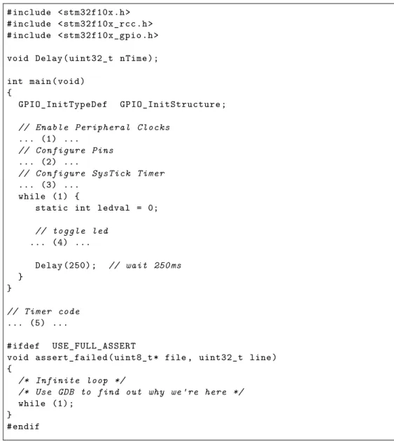
The STM32 processors are complex systems with many peripherals. Be-fore any of these peripherals can be used they must be configured. Some of this configuration is generic – for example clock distribution and pin config-uration – while the rest is peripheral specific. Throughout this chapter, we utilize a simple “blinking lights” program as a guiding example.
The fundamental initialization steps required to utilize any of the STM32 peripherals are:
1. Enable clocks to the peripheral
2. Configure pins required by the peripheral
3. Configure peripheral hardware
firmware library will perform extensive parameter checking. In the event of an assertion violation, GDB can be used to examine the parameters of this routine to determine the point of failure.
# include <stm32f10x .h> # include <stm32f10x_rcc .h> # include <stm32f10x_gpio .h>
void Delay( uint32_t nTime);
int main(void) {
GPIO_InitTypeDef GPIO_InitStructure ;
// Enable Peripheral Clocks
... (1) ...
// Configure Pins
... (2) ...
// Configure SysTick Timer
... (3) ... while (1) {
static int ledval = 0;
// toggle led
... (4) ...
Delay (250) ; // wait 250 ms
} }
// Timer code
... (5) ...
#ifdef USE_FULL_ASSERT
void assert_failed ( uint8_t * file , uint32_t line) {
/* Infinite loop */
/* Use GDB to find out why we 're here */
while (1); }
#endif
Figure 4.1: Blinking Lights
Port C with the following library command (described in greater detail in Section 4.1).
RCC_APB2PeriphClockCmd ( RCC_APB2Periph_GPIOC , ENABLE ); // (1)
After enabling the clocks, it is necessary to configure any required pins. In this case, a single pin (PC9) must be configured as an output (described in greater detail in Section 4.2).
/* (2) */
GPIO_StructInit (& GPIO_InitStructure ); GPIO_InitStructure . GPIO_Pin = GPIO_Pin_9 ;
GPIO_InitStructure . GPIO_Mode = GPIO_Mode_Out_PP ; GPIO_InitStructure . GPIO_Speed = GPIO_Speed_2MHz ; GPIO_Init (GPIOC , & GPIO_InitStructure );
Once configuration is complete, the pin can be set or reset with the following code:
/* (4) */
GPIO_WriteBit (GPIOC , GPIO_Pin_9 , ( ledval ) ? Bit_SET : Bit_RESET ); ledval = 1 - ledval ;
The blinking light demo also utilizes a “timer tick” to measure the passage of time. While this timer tick utilizes interrupts, which we will not be discussing until Chapter 11, the actual use here can be treated simply as an idiom. The Cortex-M3 core used in the STM32 processors has a dedicated timer for this function. The timer as a multiple of the system clock (which is defined in ticks/second) – here we configure it for 1 msec interrupts (the constantSystemCoreClockis defined in the firmware library to be the number of system clock cycles per second):
/* (3) */
if ( SysTick_Config ( SystemCoreClock / 1000)) while (1);
Every 1 msec, the timer triggers a call to the SysTick_Handler. For the blinking light demo, we simply decrement a shared counter – declared as
/* (5) */
static __IO uint32_t TimingDelay ;
void Delay( uint32_t nTime){ TimingDelay = nTime; while ( TimingDelay != 0); }
void SysTick_Handler (void){ if ( TimingDelay != 0x00)
TimingDelay --; }
This simple blinking lights program requires support from two library modules (stm32_gpio.c, stm32_rcc.c). To include these in the project, we have to slightly modify the Makefile provided with the demo project.
TEMPLATEROOT = ../../ stm32vl_template
# additional compilation flags
CFLAGS += -O0 -g ASFLAGS += -g
# project files
OBJS= $( STARTUP ) main.o
OBJS += stm32f10x_gpio .o stm32f10x_rcc .o
# include common make file
include $( TEMPLATEROOT )/ Makefile . common
In the remainder of this chapter we examine clock and pin configuration in greater detail.
Exercise 4.1 Blinking Lights
Complete the Blinking lights main.c and create a project using the demo program described in Chapter 3 as an example. You should compile and run your program.
4.1. CLOCK DISTRIBUTION
4.1 Clock Distribution
In the world of embedded processors, power consumption is critical; hence, most sophisticated embedded processors provide mechanisms to power down any resources that are not required for a particular application. The STM32 has a complex clock distribution network which ensures that only those peripherals that are actually needed are powered. This system, called Reset and Clock Control (RCC) is supported by the firmware module
stm32f10x_rcc.[ch]. While this module can be used to control the main
system clocks and PLLs, any required configuration of those is handled by the startup code provided with the examples in this book. Our concern here is simply with enabling the peripheral clocks.
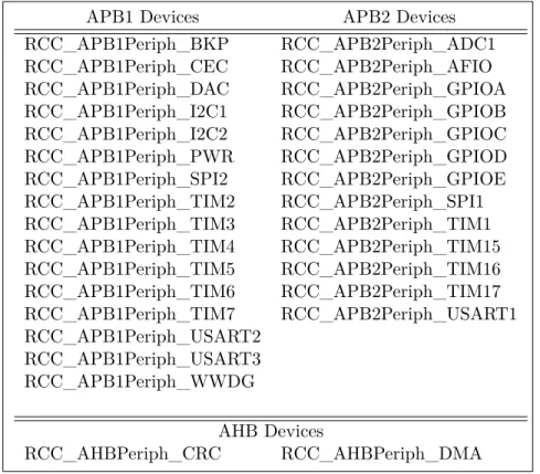
The STM32 peripherals are organized into three distinct groups called APB1, APB2, and AHB. APB1 peripherals include the I2C devices, USARTs 2-5, and SPI devices; APB2 devices include the GPIO ports, ADC controllers and USART 1. AHB devices are primarily memory oriented including the DMA controllers and external memory interfaces (for some devices)
Clocks to the various peripherals can be controlled with three firmware routines:
RCC_APB1PeriphClockCmd ( uint32_t RCC_APB1PERIPH , FunctionalState NewState )
RCC_APB2PeriphClockCmd ( uint32_t RCC_APB2PERIPH , FunctionalState NewState )
RCC_AHBPeriphClockCmd ( uint32_t RCC_AHBPERIPH , FunctionalState NewState )
Each routine takes two parameters – a bit-vector of peripherals whose state should be modified, and an action – ENABLE or DISABLE. For example, GPIO ports A and B can be enabled with the following call:
RCC_APB2PeriphClockCmd ( RCC_APB2Periph_GPIOA |
RCC_APB2Periph_GPIOB , ENABLE );