CDM Tester Properties as Deduced from Waveforms
Timothy J. Maloney* and Nathan Jack**
*Intel Corporation, 2200 Mission College Blvd., SC9-09, Santa Clara, CA 95054 USA **Intel Corporation, 2501 NW 229th Ave., RA3-402, Hillsboro, OR 97124 USA
tel.: 408-765-9389 e-mail: [email protected]
Abstract – Two-pole RLC models, matching peak current and charge under the first current peak, are shown to fit CDM waveforms well, as they target features that cause device failure. RLC properties of ferrites, air sparks, varying dielectric and other tester elements become clear and point us to a revised CDM test standard.
I. Introduction
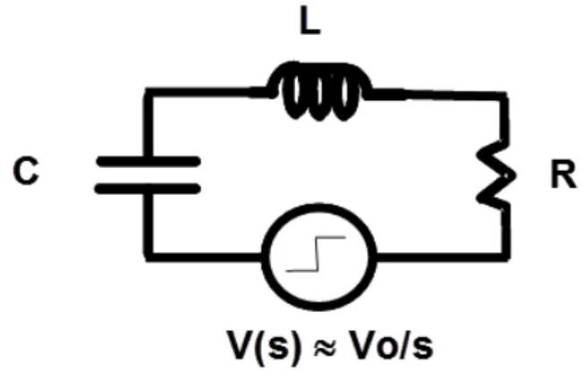
The Charged Device Model (CDM) test has, from its inception in the late 1980s, been considered essentially a discharge of a capacitor through series resistance and inductance to create an ESD current, much as pictured in the circuit model of Figure 1. Early in CDM tester and standard development, it was recognized that the “3-capacitor model” [1] collapses to a single equivalent capacitor for the sake of simplified modeling. Much work has aimed at transforming tester properties into RLC parameters for a reasonable fit to measured waveforms, but such work has forced recognition of interaction with the CDM tester chassis ground, with a resulting “5-capacitor model” (plus one more inductor) and more complicated modeling [2]. But more recently, CDM tester manufacturers have removed or weakened the chassis ground interaction, and CDM waveforms over a wide range of calibration target and package sizes can be fit better than ever using simple RLC models.
Figure 1. Two-pole RLC model of CDM pulse.
The s-domain current function for Fig. 1 is
1
)
(
2 0+
+
=
RCs
LCs
CV
s
I
, (1)s=σ+jω, and the poles p1,2 are such that
)
1
(
20 2 ,
1
=
−
D
±
D
−
p
ω
(2)where
ω
0=
1
/
LC
,
D
=
ω
0RC
/
2
and commonly called the damping factor [3]. The waveform will be a damped sinusoid (D<1), with a complex conjugate pole pair, or a double exponential (D>1). Smaller components tend to be underdamped in CDM because D decreases with capacitance.II. RLC Calculation
The general outline of the RLC calculation is shown in Figure 2, where we start with measured waveform properties like charging voltage V0, first peak charge Qfp, final charge Qa (=C0V0) and peak current Imax, and use them to derive equivalent R and L, which we’ll now call Req and Leq. Along with familiar relations like CV=Q and V=IR, we are going to need two rather obscure properties of the two-pole RLC circuit for extraction of the equivalent circuit from the waveform. The first applies to the smaller devices, for D<1, where we note the ratio of Qfp to Qa, which can be shown (see Appendix A) to depend entirely on damping factor D:
. (3)
Thus the ratio allows immediate calculation of D.
Figure 2. Flow of RLC calculation for D<1, with Req, Leq and Co corresponding to quantities in Fig. 1.
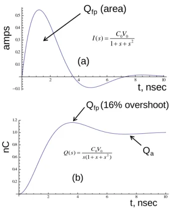
Figure 3a shows what we mean by Qfp (=V0Cmax) for a computed D=0.5, ω0=1 GHz, and 1 nC of charge Qa, while Fig. 3b integrates that waveform, showing Qfp at the peak. As D approaches 1 or becomes greater than 1 for the larger CDM targets, the integrated charge due to undershoot becomes small to nonexistent, so this ratio method becomes ineffective. But at that point the centroid method [4] becomes less sensitive to undershoot effects and can better help to find D. We will return to that topic.
Clearly we are closing in on exactly capturing the first peak charge Qfp, one of our important quantities. The other one, Imax, can be used to determine Req now that we know D, because it can be shown that
(4),
as discussed in Appendix B. The hyperbolic arctangent of Eq. (4) applies to D>1. As in Appendix B, the coefficient of V0/Req is a function g(D) that
goes from 0 to 1, as D∞ is the well-known one-pole RC decay with current at t=0+ of V0/Req. Figure 4 shows the behavior of g(D).
Figure 3. Computed waveform (a) and integrated waveform (b) showing 16% overshoot of the final charge for D=0.5; s in GHz.
Figure 4. Behavior of CDM Imax current function g(D), showing fraction of V0/R reached.
At this point we have pegged Req to Imax and D to Qfp, and have found C0 from total charge, so Leq is determined from the definition of D (Fig. 2) and we have a complete RLC model, one guaranteed to match the peak current Imax and the first peak charge Qfp.
III. Experimental Results
1. C
0versus Package Size
The intent of this study is to allow better prediction of the CDM waveform and essential properties, given a Qa
Qfp Vo Imax
Co
Leq D
Cmax
Req
derived quantity measured quantity
LC RC D
2
=
am
ps
2 4 6 8 10
0.1 0.1 0.2 0.3 0.4
0.5
Q
fp(area)
t, nsec
2 0 0
1 ) (
s s
V C s I
+ + =
(a)
2 4 6 8 10
0.2 0.4 0.6 0.8 1.0 1.2
Q
fp(16% overshoot)
nC
t, nsec
) 1 ( )
( 0 0 2 s s s
V C s Q
+ +
=
Q
a(b)
0 0.2 0.4 0.6 0.8 1
0 1 2 3 4 5
g(
D)
D -- Damping factor
Imax= g(D) *V0/Req
1
),
1
exp(
1
2
<
−
−
+
=
D
D
D
Q
Q
a
fp
π
)) 1
( ) h tan( 1
exp(
2 1 2
2 0
max
D D
D D D
R V I
eq
−
− −
device to be tested. If we start with a package area and want to know a worst case C0 (effective capacitance from integrated “fast” current), the size trend with metal target area should be sufficient. Packages of similar area that add dielectric should have smaller C0, and a single Vss pulse could yield its exact C0 value. The trend of C0 with target size within our range of interest of sizes is empirically simple, as seen in Figure 5 with a square root dependence on area. Values for 250V nearly coincide with 500V, as expected. Dielectric was the standard JEDEC 15 mils (0.381 mm), as is the case in all this work unless otherwise stated.
Figure 5. Effective CDM capacitance vs. metal target size. JEDEC circular targets are the first and third nonzero points, while P4 and P6 circular targets are the second and fourth.
C0 is a series-parallel combination as shown in the 3-cap model [1,2], and calculations including fringing capacitance confirm this trend. We now can correlate C0 with package size.
2. Standard JEDEC Tester
When 8 GHz waveforms from standard JEDEC testers were analyzed as in Section I, we found, remarkably, that resistance goes up as target size decreases, but in orderly fashion (Figure 6), due to a constant slope and non-zero intercept. When tau=ReqC0 is plotted against C0, it appears that we can predict Req=[20.6+68.7 psec/C0(pF)] ohms for 250V.
The slope-intercept fit was also found at 500V (Figure 7), but with a higher slope (27.5 ohms) and not much smaller intercept (56.8 psec). This was over an even wider range of capacitance (i.e., metal target size) and at a different company. Measurements on four targets at Intel gave 27.8 ohms at 500V, closely agreeing with Fig. 7. The inductance Leq (Figs. 6-7) completes the model and varies as shown. There is slightly higher average Leq (11.9 nH) for 500V, plus a downward trend with C0 that could be traceable to spark rise time. With these trends in Req, Leq, and C0, plus the prediction of C0 from package size, we have a way to
predict JEDEC waveforms and their properties over a wide variety of packages.
Figure 6. Req on Intel Orion2 tester follows slope-intercept form for the four targets of Fig. 5. Inductance varies as shown.
Figure 7. Req on Orion2 JEDEC tester also follows slope-intercept form, using seven targets of various sizes. Inductance varies as shown. Data used with permission and provided by M. Johnson, Texas Instruments.
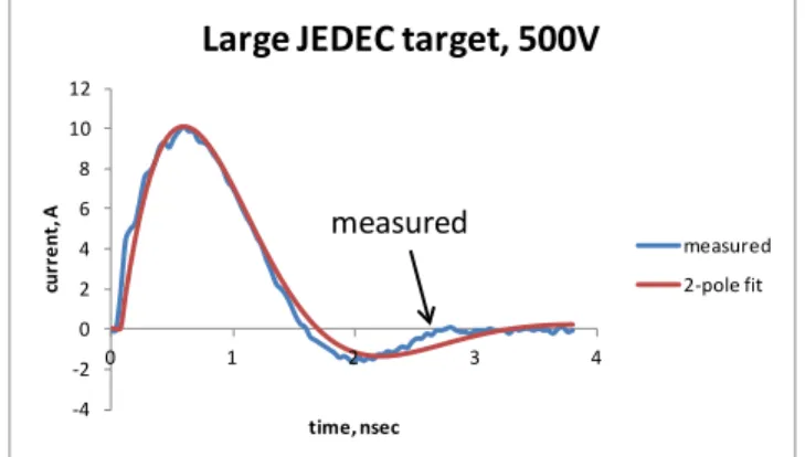
Figure 8. Measured and 2-pole waveforms for large JEDEC target in Intel Orion2 tester, 500V.
Figure 8 shows an example of how well the modeling method fits a measured (8 GHz scope) waveform. The Fig. 8 waveform was taken on an Orion2 JEDEC tester at 500V and uses parameters of Req=28.6 ohms, C0=16.28 pF, and Leq=11.69 nH in order to match Imax and Qfp exactly.
y = 0.6696x
0 5 10 15 20 25 30
0 10 20 30 40 50
Co
, p
F
Sqrt(Area), mm
Co vs. Pkg Size
250V 500V Linear (500V)
y = 20.562x + 68.704
0 100 200 300 400 500 600
0 5 10 15 20 25
ta
u=
Re
q*
Co
, p
se
c
Co, pF
Orion2, 250V
Leq=10.33±1.49 nH
y = 27.482x + 56.849
0 100 200 300 400 500 600 700 800
0 5 10 15 20 25 30
ta
u=
Re
q*
Co
, p
se
c
Co, pF
Orion2, 500V
Leq=11.9±2.54 nH
-4 -2 0 2 4 6 8 10 12
0 1 2 3 4
cu
rr
en
t, A
time, nsec
Large JEDEC target, 500V
measured 2-pole fit
3. FFPA trials
In recent times, Intel participated in the efforts of the JEDEC/ESDA CDM standards committee members (including Analog Devices and two locations at Texas Instruments) to vary the thickness of the dielectric over the field plate from 14 to 59 mils (0.36-1.5mm) for the small and large JEDEC targets. 8 GHz data at around 500V on modified testers without a ferrite (FFPA or ferrite-free probe assembly) were acquired and analyzed. Thicker dielectric, it was hoped, would lower Imax for our desired test voltages in the absence of the ferrite, and thus make testers more reproducible. However, the absence of a ferrite seemed to lower the 510V Req slope somewhat (20.6 ohms; see Figure 9) and lowered the Leq to the ranges shown, averaging 3.5 nH, much as calculated for the metal probe itself. But the tau vs. C0 plot correlated extremely well, as seen in Fig. 9. Imax decreased due to lower C with thicker dielectric in accordance with the g(D) function (Fig. 4) but the lower Req and Leq outweighed that effect and delivered high Imax currents. A similar effect with the low Leq was seen with a CDM fixture having 10 ohm resistance to ground (instead of 1 ohm) from the probe—even with 10 ohms added to the spark resistance, Imax currents were off-target as far as preserving the JEDEC CDM legacy [5]. Some other way of approximating the JEDEC CDM test was needed.
Figure 9. Req on RCDM3 tester with dielectric thickness variation for two JEDEC targets; lower C0 with thicker dielectric.
Average inductance Leq is given for each group. Data from JEDEC/ESDA CDM standards committee; used with permission.
4. Air Spark and 25 ohm Series Resistance
The Orion2 CCDM (contact CDM, also called CDM2 [6]) test head can also be used in air spark mode, although this adds 50 ohms to the air spark. The CDM discharge waveform ends up having much charge in a long, extended tail, apparently because the spark breaks up in its later stages due to the weaker driving force of the 50 ohms. But with a 25 ohm load from probe to ground instead of 50 ohms, these
effects were much reduced and the results much closer to reproducing the JEDEC CDM legacy.
The 25 ohm termination of the CCDM test head probe was achieved with an SMA tee on the test head, terminating one branch with 50 ohms and the other with a 50 ohm cable to the oscilloscope 50 ohm input and attenuator as usual. This places the 25 ohm load at the end of a 2-3 cm 50 ohm coaxial line inside the CCDM test head, an inductive termination that may or may not be desired.
Figure 10. Req tau plot for 25 ohm termination on Orion2 CCDM test head, showing 48.9 ohm slope for both 250 and 500V. Average inductance Leq is 11.62 nH.
Figure 10 shows that the 25 ohm load adds an average of 25 ohms to a spark of about 24 ohms for both test voltages, and that Leq is about 11.6 nH. This is in the range of the ferrite-equipped JEDEC test head Leq, with extra inductance evidently due to the mismatch of the embedded 50-ohm line. An example of waveform match to the RLC fit is shown in Figure 11.
Figure 11. Waveform and 2-pole fit for small JEDEC target on 25-ohm-terminated CCDM fixture with air spark, 500V. C0=4.57
pF, D=0.4606, ω0=4.007 GHz, so Req=50.3 ohms, Leq=13.6 nH.
The true test of the 25-ohm scheme’s utility is comparison with the JEDEC CDM tester for critical parameters like Imax and Qfp, as in Figure 12. The same four targets as in Figs. 5-7 were used. The red small target
large target Leq=2.39±0.6nH Leq=4.26±0.4nH
Leq=11.62±1.16 nH
-2.0 -1.0 0.0 1.0 2.0 3.0 4.0 5.0 6.0
0 1 2 3
cu
rr
en
t, A
time, nsec
25 ohms, small JEDEC target
measured 2-pole fit
arrows show the presumed linear path in Imax-Qfp space that would be traversed going from 250 to 500V for the 25-ohm test. It is clear that the exact Imax and Qfp conditions of 250V JEDEC cannot be reproduced by 25 ohms for all target sizes. However, Imax or Qfp can always be hit by varying precharge voltage to somewhere between 250 and 500V, depending on target size. For a least-squares fit to both Imax and Qfp, one would first normalize the chart scales for each target JEDEC value (triangles in Fig. 12), and adjust for any weighting factors being applied to Imax and Qfp. Then drop a perpendicular from the target triangle to the line connecting 250 to 500V 25-ohm values; the associated voltage represents the closest approach to the target values of Imax and Qfp.
Figure 12. 25-ohm results for two voltages and JEDEC for 250V, plotted in the plane of Imax and Qfp. JEDEC data from M. Johnson, Texas Instruments.
5. CCDM or CDM2
An analysis of 500V small and large JEDEC target calibration waveforms for the CCDM/CDM2 test fixture under ordinary use (relay and 50 ohm cable) showed Req≈55 ohms for both targets and Leq≈3.9 nH for the large target, where little influence due to relay spark rise time is expected (small target Leq was 6.45 nH). In any case, under these Z-matched and no-air-spark conditions, the fixture shows the expected resistance and Leq consistent with no ferrite. A 25 ohm CCDM test might give even closer agreement with JEDEC than the 50 ohm. Prospects for mapping multiple targets and voltages for comparison with JEDEC, as in Fig. 12, are good.
IV. Discussion: Damping Factor
Trends and Spark Burn Rate
Another way to examine the variation of Req and Leq as C0 varies is to look at how D varies. We might expect from the definition of D (in Fig. 2, forexample) for it to increase as the square root of C0, but that is not really the case.
Figure 13 shows two examples, with data from earlier figures, of damping factor D vs. C0, and the tendency of D to settle around a mid-range of mildly underdamped values. This is clearest in Fig. 13b, where the break between large and small JEDEC targets was why we could not acquire data in the C0 range where the plateau seems to be. Even so, Fig. 13 suggests that D is compressed into a mid-range and may “break out” to higher or lower values at high or low capacitance, but clearly does not follow √C0, as would be the case if Req and Leq remained constant. Why might this be?
Figure 13. Damping factor trends for (a) JEDEC targets as in Fig. 7 (data from M. Johnson, Texas Instruments) and (b) FFPA dielectric thickness data as in Fig. 9 (data from JEDEC/ESDA CDM committee). D clusters around mildly underdamped values.
The answer could be in the physics of the electrostatic spark plasma, which after all has a “resistance” based on its ability to create heat, light, sound, excited atoms and molecules, etc., in a short period of time, with energy supplied by the collapsing fields. The total field energy goes down as the plasma burns energy, but as the event progresses, the field energy is partitioned between electric and magnetic fields. The current i(t) drains the electric field initially stored in C, but is limited by magnetic field storage proportional to L. We therefore expect the RLC
sm P4 lg P6
(a)
0 0.2 0.4 0.6 0.8 1 1.2
0 2 4 6 8 10 12 14
da
m
pi
ng
fa
ct
or
, D
Co, pF
D vs. Co, dielectric thickness variation
network’s time constant √LC to determine how fast the field energy can be dissipated.
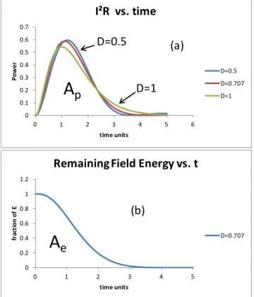
For low damping factor D approaching zero, the 2-pole RLC circuit rings for a long time and does not dissipate field energy very fast compared with time scale √LC. The same is true of high D>>1, where the capacitor discharges slowly. There must be an intermediate D at which the field energy burns off as fast as possible, on the order of time scale √LC. That D is 1/√2, as shown in Appendix C, if the energy decay time is measured by integrating the (normalized) remaining field energy over time, starting with the beginning of the spark discharge.
Figure 14. (a) Dissipation rate vs. time (in √LC units) for three values of damping factor D. For each curve the normalized initial field energy Ap=1. (b) Remaining fraction of electric and
magnetic field energy vs. time for optimized value D=1/√2; dissipation time Ae=√2 time units, lower than any other D.
Figure 14 shows what happens with power dissipation (i2(t)Req) and remaining field energy versus time, where time is in normalized units of √LC as described in the appendices, for three values of D. The area Ap in Fig. 14a is the same for all D because it is the initial field energy C0V02/2, normalized to one. But there are subtle differences among curves for D=0.5, 0.707..., and 1.0, such that the first moment (centroid) of the middle one, for D=0.707..., is minimum (see Appendix C). This quantity (in normalized time units) is the area Ae in Fig. 14b and is 1.414... or √2 for D=1/√2, while it is 1.5 for D=0.5 and D=1. Thus
the maximum plasma burn rate, for fixed resistance,
occurs when D=1/√2 or R= 2L/C .
However, if time-variant R(t) (equivalently, D(t)) is allowed, one can easily beat the Ae=1.414… time units of Fig. 14b through numerical solutions of the normalized RLC network equation
0 ) ( ) ( ) ( 2 )
( + ′ + =
′′ t D t q t q t
q , (5)
where q(0)=1 and q’(0)=0; q being charge and q’ the current. For example, when D(0)=0.5 and exponentially approaches D=1/√2 with a time constant of 1 (meaning that D<0.7 for the bulk of the pulse), we get a time constant (area Ae) of only 1.39 time units. This trial was inspired by finding that D≈0.55 produces maximum power dissipation at Imax. The optimal solution, if unique, is not yet known but is likely to be better than 1.39. But any mathematically ideal solution also has to merge with “reasonable” physical conditions in the plasma. For example, the spark initiates through ionization and the resistance comes down from infinity in a short period of time [7], although sometimes we account for this in the circuit model by introducing extra poles to describe the rise time of the spark [8,9]. While the spark rise time is believed to be only tens of picoseconds, maximum burn rate of the field energy may describe the bulk of the nanosecond-scale CDM discharge time. We now discuss why this could be reasonable.
The idea of minimizing Ae in Fig. 14b suggests some kind of Least Action Principle as in Lagrangian mechanics [10], as Action is defined as Energy×Time. The integral Ae of field energy over time is indeed a minimum (√2) for D=1/√2, as discussed above, when D(t) is constant, and is known to be lower for some D(t). But it is more intriguing to consider why this maximum burn rate of field energy might happen to the spark plasma: Maximum burn rate should also mean a maximum rate of increase of entropy in the system, as the spark plasma produces heat. The spark plasma system, while certainly not in equilibrium, does evolve toward a most likely state, in accordance with the definition of entropy in statistical mechanics. It is thus not surprising to see a spark plasma adopt a maximum burn rate when that rate is not constrained by other processes in the plasma. Those processes, like the spark rise time discussed above, may often be fast enough to allow very close to the maximum burn rate for the nanosecond-scale CDM event.
The concept of least action and of maximum entropy in dissipative Lagrangian systems has been examined over the last century or more (Lord Rayleigh is often 0
0.1 0.2 0.3 0.4 0.5 0.6 0.7
0 1 2 3 4 5 6
Po
w
er
time units
I²R vs. time
D=0.5 D=0.707 D=1
A
p
D=0.5
D=1 (a)
0 0.2 0.4 0.6 0.8 1 1.2
0 1 2 3 4 5
fr
ac
tio
n o
f E
time units
Remaining Field Energy vs. t
D=0.707
(b)
cited on dissipation) and is still a subject of discussion and research. One recent author [11,12] has even produced work on least action and its ties to maximum entropy and stochastic mechanisms in systems in and out of equilibrium. We will not attempt to resolve any of these long-standing controversies. But our data in Fig. 13 do offer something for the theorists to consider—a possible example of a dissipative system that is driven by easily understood physical principles to behave in a certain quantifiable way. Fig. 13 suggests that if the physical conditions are right—plasma processes on a much shorter time scale than √LC for example—the damping factor D assumes values near those associated with maximum burn rate of the field energy, for a large range of capacitance C0.
V. Conclusions
A new calculation method makes 2-pole RLC fits to measured CDM waveforms by prioritizing the matching of peak current Imax and first peak charge Qfp. This is applied to various CDM data and allows accurate prediction of CDM waveforms and properties following a few measurements, while also inspiring explanations of many previous observations. We were very inspired by certain previous CDM studies [2,13] and yet noted that the present methods offer significant new benefits to contemporary CDM workers who undertake modeling:
1. Capacitance C0 is likely to correlate to the square root of area for comparable objects, e.g., the metal calibration targets and packages with similar amounts of extra dielectric.
2. The variation of equivalent resistance Req with C0 is best studied by plotting ReqC0 vs. C0 to give a slope-intercept linear form. The linear fit, at least for metal targets, can have an astoundingly high correlation coefficient (R2=0.997 in one case) and has been observed with and without ferrites in the CDM fixture. Variations in equivalent spark resistance thus became much less mysterious.
3. Inductance Leq has some scatter over the full range of C0 values for a given configuration, but is usually stable, and the effect of a ferrite in the CDM fixture— raising Leq and Req—is easily observed.
4.Trends in the damping factor (D=ReqC0/[2√LeqC0]) are easily tracked and plotted, given that all the new calculations can be captured on an Excel spreadsheet after a few key parameters are extracted from each waveform. Over a considerable C0 range, D was seen to be compressed toward values indicating maximum possible dissipation rate of field energy by a resistor.
We think D should be watched for further revealing evidence.
The use of a 25-ohm series resistance in a ferrite-free probe assembly was fairly successful in reproducing JEDEC-like CDM conditions as long as plate voltage could be varied to match JEDEC Imax and first peak charge Qfp. This was done with the air spark in series, giving Req≈50Ω. The same 25-ohm coaxial resistance could possibly be used in CDM2/CCDM [6] to simulate the air spark reproducibly and achieve even closer agreement with JEDEC waveforms, given also that there would be a mismatched 50-ohm line segment in the CDM2/CCDM fixture that could provide extra equivalent inductance. These continuing studies suggest that a more reproducible CDM test could be achieved without much departure from the JEDEC CDM legacy.
Appendix A: First Peak Charge
For D<1, we start with the expression for CDM current for Fig. 1 as recorded by [2] from many textbooks, including [14]:)
sin(
)
(
0t
e
L
V
t
i
atω
ω
⋅
⋅
=
−, (A.1)
where L
R a
2
=
,
2 2 0
−
a
=
ω
ω
(A.2) and ω0=1/√LC, as below Eq. (2). In terms of D and
ω0,
)
1
sin(
1
2
)
(
0 22
0
e
0D
t
D
D
R
V
t
i
Dt⋅
−
−
⋅
=
−ωω
)
1
sin(
1
2 0
2 0
0
e
0D
t
D
C
V
Dt⋅
−
−
=
ω
−ωω
. (A.3)
From standard tables, the current integrated from 0 to
∞ is Qa=CV0, as expected. Note also that time can be normalized to units of 1/ω0, with simpler expressions if we allow ω0=1. To find Qfp, the charge under the first peak or first half cycle, we want
dt t D e
D CV Q
D Dt
fp
∫
−
− ⋅ −
− =
2
1
0
2 2
0
) 1 sin( 1
π
. (A.4)
Again with the help of standard integral tables, this is
2
1
0 2
2
2 2
2 0
1
)]
1
cos(
1
[
1
D Dt
fp
D
D
t
D
D
e
D
CV
Q
− −
−
+
−
−
−
−
=
− − + = 2 0 1 exp 1 D D CV
π
, (A.5) in accordance with Eq. (3).
Appendix B: Peak Current
The CDM current for the circuit in Fig. 1 will peak at the first occurrence of di(t)/dt=0. Differentiating Eq. (A.3) for D<1 means that Imax occurs when) 1
sin( 0 2 0
0D −D t
−
ω
ω
0 ) 1
cos(
1 2 0 2 0
0 − − =
+
ω
Dω
D t , or (B.1)D
D
t
D
2 0 2 01
)
1
tan(
ω
−
=
−
. (B.2)
Again, using normalized time units and allowing ω0=1 will not affect the answer. Substituting the peak current time t0 back into Eq. (A.3), we get
)) 1 ( tan 1 exp(
2 1 2
2 0 max D D D D D R V I − − − = − , (B.3)
in accordance with Eq. (4) for D<1. For D>1, a similar derivative is sought, as there is a sinh expression for the current replacing sin, tanh for Imax, and D2-1 replacing 1-D2, still a positive quantity. Note that Imax is always a fraction g(D) of V0/R:
)
(
0max
g
D
R
V
I
=
,
−
−
−
=
−)
1
(
)
h
tan(
1
exp
2
)
(
2 1 2D
D
D
D
D
D
g
. (B.4)At D=1, i(t) is of the form te-t and g(1)=2/e. g(D) is plotted in Fig. 4 of the text.
Appendix C: Maximum Burn
Rate of Field Energy
Power dissipation in the CDM spark is i2(t)R, and its integral over time will be equal to the initial field energy Qa2/2C. This integral can also be used to show the remaining fraction of field energy, electric and magnetic, versus time. As described in the text, we are interested in the value of R (proportional to D) giving the fastest dissipation of the field energy, and will measure that speed with the time integral of the remaining fraction of field energy. We would like to
minimize this field collapse time given a choice of L and C, and for simplicity, we will consider a fixed D. We expect some kind of time-variant D (i.e., R) to give the lowest value of field collapse time, but will not attempt a rigorous global solution.
Starting with Eq. (A.1) for i(t) and again (since L and C are fixed) using normalized time units of 1/ω0, we have
)
1
(
sin
)
(
)
(
t
i
2t
R
De
2 2D
2t
P
=
∝
− Dt⋅
−
))
1
2
cos(
1
(
2 2t
D
e
Dt−
−
∝
−. (C.1)
Proportionalities are sufficient since we simply want to examine time dependence on D and minimize the decay time of the field energy, found by integrating P(t) and noting the rise time. The last expression in Eq. (C.1) converts to the s-domain when we consult a table of Laplace Transforms [15]:
2 2 4 4 ) 2 ( 2 2 1 ) ( D D s D s D s s P − + + + − + ∝ 4 1 2 1 2 1 2 s Ds D s B D s A + + + − +
= , (C.2)
where A=1/2D, B=D/2. In the s-domain, the dissipated energy E(s)=P(s)/s, so the essentials are in Eq. (C.2). To find the rise time of consumed energy E(s) (equal to field collapse time), we consider the Elmore Delay of (C.2) by finding the s-coefficient of its normalized series expansion, as done in [3,4] and many other references. After some manipulation, (C.2) becomes + + + + + − − + − ∝ ) ( 2 1 1 ) ( / 1 ) ( ) ( 2 2 s O s D D s O s B A D B AD B A s P . (C.3)
However, note that AD-B/D=0. Thus our time constant is the s-coefficient of the denominator,
D D e 2 1 + =
τ
, (C.4)
which is minimum (√2 time units) at D=1/√2=0.707…. Note also that τe=1.5 at D=0.5 and D=1, and that D=1/√2 is their geometric mean. Thus we have proven that the slightly underdamped D=1/√2
or R= 2L/C produces “maximum burn rate” of the field energy by a fixed resistance. Curiously, this
quality factor Q=1/2D=D) has been called a pseudo-Gaussian and has been a favorite for approximating oscilloscope filtering of signals [3,16].
Acknowledgement
The authors would like to thank Alan Righter, Analog Devices, Scott Ward, Texas Instruments (Dallas), Marty Johnson, Texas Instruments (Santa Clara), and Marti Farris of Intel. As members of the JEDEC/ESDA CDM Standards committee, they provided CDM data as noted in the text, and gave their permission to publish it here.
References
[1] R. Renninger, M-C. Jon, D.L. Lin, T. Diep and T.L. Welsher, “A Field-Induced Charged-Device Model Simulator”, 1989 EOS/ESD Symposium Proceedings, pp. 59-71, 1989.
[2] B.C. Atwood, Y. Zhou, D. Clarke, and T. Weyl, “Effect of Large Device Capacitance on FICDM Peak Current”, 2007 EOS/ESD Symposium Proceedings, pp. 273-282.
[3] T.J. Maloney and A. Daniel, "Filter Models of CDM Measurement Channels and TLP Device Transients", 2011 EOS/ESD Symposium Proceedings, pp. 386-394. See https://sites.google.com/site/esdpubs/documents/e sd11.pdf.
[4] T.J. Maloney, "HBM Tester Waveforms, Equivalent Circuits, and Socket Capacitance", 2010 EOS/ESD Symposium, pp. 407-415. See https://sites.google.com/site/esdpubs/documents/e sd10.pdf.
[5] A. Righter, et al., “Progress Towards a Joint ESDA/JEDEC CDM Standard: Methods Experiments, an Results”, 2012 EOS/ESD Symposium Proceedings, pp. 32-41.
[6] R. Given, M. Hernandez, and T. Meuse, “CDM2—A New CDM Test Method for Improved Test Repeatability and Reproducibility”, 2010 EOS/ESD Symposium Proceedings, pp. 359-367.
[7] R.G. Renninger, "Mechanisms of Charged-Device Electrostatic Discharges", 1991 EOS/ESD Symposium Proceedings, pp. 127-143.
[8] T.J. Maloney, "Easy Access to Pulsed Hertzian Dipole Fields Through Pole-Zero Treatment", cover article, IEEE EMC Society Newsletter, Summer 2011, pp. 34-42. See
http://ewh.ieee.org/soc/emcs/acstrial/newsletters/s ummer11/index.html.
[9] Timothy J. Maloney, “Antenna Response to CDM E-fields”, 2012 EOS/ESD Symposium Proceedings, pp. 268-278. See https://sites.google.com/site/esdpubs/documents/e
sd12.pdf.
[10] H. Goldstein, Classical Mechanics (Reading, MA: Addison-Wesley, 1950).
[11] Q.A. Wang and R. Wang, "Is it Possible to Formulate Least Action Principle for Dissipative Systems?", http://arxiv.org/abs/1201.6309v5, 10 July 2012.
[12] Q.A. Wang, "Is There Least Action Principle in Stochastic Dynamics?", http://hal.archives-ouvertes.fr/docs/00/14/14/82/PDF/Virtualwork_le astaction.pdf, 2007.
[13] R.E. Carey and L.F. DeChiaro, "An Experimental and Theoretical Consideration of Physical Design Parameters in Field-Induced Charged Device Model ESD Simulators and Their Impact Upon Measured Withstand Voltages", 1998 EOS/ESD Symposium Proceedings, pp. 40-53.
[14] H.H. Skilling, Electrical Engineering Circuits
(New York: John Wiley & Sons, 1959), pp. 472-477.
[15] M. Abramowitz and I.A. Stegun, Handbook of Mathematical Functions, (New York: Dover Publications, 1965).