Pv Based Interline Dynamic Voltage Restoring Device For
Mitigation Of Power Quality Problems
1
Mr. Gouse Mohiddin Khan,2Mr. K.Ashok Kumar 1
P.G student, EEE, BVC INSTITUTE OF TECHNOLOGY AND SCIENCE, BATLAPALAM, A.P 2Asst.Prof, EEE, BVC INSTITUTE OF TECHNOLOGY AND SCIENCE, BATLAPALAM, A.P
Abstract— Now a days the renewable energy sources importance has increased in the distribution system. In this paper an interline dynamic voltage restorer (IDVR) has proposed for the distribution systems to mitigate voltage sag/swell problems and improve power quality. In general for the normal voltage levels, the DVRs should be bypassed. Instead of bypassing the DVRs, this paper proposes new operating scheme for the DVRs, if needed, to improve the displacement factor (DF) in any one of the involved feeders. Generally an interline dynamic voltage restorer consists of several dynamic voltage restorers (DVRs) with a sharing dc link. IDVR is connected to the independent feeders to secure the electric power to the critical loads. One of the DVRs compensates for the local voltage sag in its feeder, and the other DVRs replenish the common dc-link voltage is supplied by using solar energy (PV). DF improvement can be achieved via active and reactive power exchange (PQ sharing) between different feeders. To validate the proposed system, Simulation results have been presented using MATLAB/SIMULINK software.
Index Terms— PV system, Displacement factor improvement, IDVR, IVDFC, PQ sharing mode.
I. INTRODUCTION
Distribution networks are mostly inductive at the fundamental frequency because of the nature of the dominant connected loads (e.g., induction motors). This, in turn, reduces the displacement factor (DF) and places an additional burden on the electrical supply. Low DF operation is not recommended due to several negative effects on the power system including:
1) Higher current for a given active power and a corresponding increase in total copper loss (i.e., system efficiency decrease);
2) lower utilization of power system components;
3) Voltage regulation issues and rising power delivery costs.
Several practical techniques are commonly used to improve DF. DF improvement employing capacitor banks with size and location optimization has been introduced in. The optimal location and size of the capacitor bank to be placed in radial distribution feeders to improve their voltage profile and to reduce the total energy loss are presented in [3]. Different techniques are employed in [4] to minimize the power loss in distribution networks. In [5], the feeder reconfiguration concept in distribution systems is introduced
to reduce system loss. In [6], a combined system for harmonic suppression and reactive power compensation is proposed not only to improve the DF but also the power factor.
A Statcom can be used as a viable alternative for DF improvement. Suitable adjustment of the phase and magnitude of the STATCOM output voltages enable effective control of active as well as reactive power exchanges between the STATCOM and the distribution system. Such a configuration allows the device to absorb or generate controllable active and reactive powers. A STATCOM has various features, including fast response, low-space requirement, and good stability margins. Recently, it is rapidly replacing the conventional naturally commutated reactive power controllers and static VAR compensators. The reactive power supplied by the STATCOM for DF improvement is capacitive in nature. Intuitively, the higher theSTATCOM’s reactivepower, the higher the dc-link voltage of the STATCOM (the higher the voltage requirements of the semiconductor devices).
The DVR is one of the most common and effective solutions for protecting critical loads against voltage sag. The DVR is a power electronic device used to inject three-phase voltages in series and in synchronism with the distribution feeder voltages in order to compensate for voltage sags. Moreover, it can be effectively used to enhance the fault ride through capability in wind applications. Detection time is an important factor in the voltage restoration process. Fast detection algorithms and effective control schemes for a DVR are proposed in [16] and [17], respectively. Space vector modulation (SVM) is the recommended modulation scheme in a DVR due to its simple digital realization and improved dc-link utilization.
In distribution systems, load voltage restoration can be achieved by injecting active and/or reactive power into the distribution feeder. Active power capability of the DVR is governed by the capacity of the energy storage element and the employed compensation technique. Several control techniques have been proposed for voltage sag compensation, such as pre-sag, in-phase, and minimal energy control approaches. If the required power for voltage restoration is obtained from the neighboring feeder(s), the compensating device is technically called an interline dynamic voltage restorer (IDVR).
(P1 and P2 ) and active power transfer between lines (P12). With respect to the line current, the injected voltage has two components. The quadrature component provides reactive power compensation for the line, while the in-phase component absorbs or generates the required active power.
The main differences between an IPFC, IDVR, and the proposed system are summarized in Table I. In this table, the IPFC, which is used in transmission applications, is compared with an IDVR and IVDFC, which are considered for distribution systems. It should be noted that the IPFC was the inspiration for proposing the IDVR for distribution networks. The IDVR can be used to mitigate voltage sag, or swell, at critical loads in distribution systems. It consists of several back-to-back voltage source converters with common dc link connecting independent feeders as shown in Fig. 2.
Each converter can be operated in either power control (PC) or voltage control (VC) modes. If one of the feeders is subjected to voltage sag, its converter will operate in VC mode and the required power for voltage restoration will be absorbed from the dc link. In this state, the other converters connected to the healthy feeders should be switched to PC mode to replenish the dc-link voltage; a power-sharing scheme to determine the reference power of each healthy feeder is presented in [24]. The injected voltage in a healthy feeder during PC mode should have two components. The first component is in-phase with line current, which absorbs active power from the supply and provides it to the dc link to support its voltage. The second component is in quadrature with the line current and is used to avoid load voltage magnitude perturbations after voltage injection as shown in Fig. 3. In previous work, the injected voltage in a healthy feeder is emulated by using the virtual impedance.
During normal operating conditions (i.e., all feeders are healthy), the DVRs are typically bypassed via bypass switches, or they can be alternatively used for load sharing purposes as presented in [26]. Instead of bypassing the IDVR in normal operation, this paper proposes a new operational mode, namely PQ sharing mode, to improve the DF of one of the involved feeders by sharing active and reactive power among different system feeders through the buffering stage (the common dc link). To apply this concept, several constraints are observed throughout the paper. The proposed interline dynamic voltage restoring and DF controlling device (IVDFC) is supported using simulation results.
Fig. 1 Single line diagram of an IPFC in transmission system
Fig. 2 Single line diagram of multiline IDVR in the distribution system
Fig. 3 PC mode
TABLE I
SALIENT FEATURES OF THE IPFC, IDVR, AND IVDFC
II. TWO-LINE IVDFC SYSTEM IN NORMAL OPERATION
Similar to the IDVR, the two-line IVDFC simply consists of two voltage source converters connected back-to-back with a common dc link, as shown in Fig. 4. For normal voltage levels, achieving active power exchange Pex between the feeders (from sourcing feeder to receiving feeder), requires controlled voltage injection in each feeder by the corresponding converter (see Fig. 4). This injected voltage should not perturb the load voltage magnitude of both feeders; therefore, both converters are operating under PC mode.
A. Sourcing Feeder
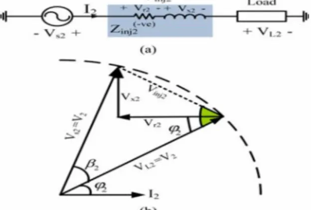
The converter in the sourcing feeder is responsible for feeding energy into the dc link via injecting a controlled voltage (magnitude and phase) through the series coupled transformer allowing for power exchange. In this paper, in order to emulate the effect of voltage injection on the feeder DF, the injected voltage is emulated using a voltage drop across series virtual impedance, as shown in Fig. 5(a). The resistive component of this virtual impedance absorbs active power (Pex) from the source, while the function of the capacitive reactance component is to maintain a constant load voltage magnitude. After voltage injection,the supply’s active power increases while it’s reactive power decreases due to the virtual injected capacitive reactance, hence, the sourcing feeder DF eventually increases. Assuming a three-phase balanced load is connected to the feeder; the per-phase equivalent circuit of the feeder with series virtual impedance injection is shown in Fig. 5(a), while the corresponding phasor diagram is shown in Fig. 5(b).
Fig. 5 sourcing feeder: (a) per-phase equivalent circuit with virtual impedance injection and (b) corresponding phasor
diagram
For a given transferred active power Pex (through dc link), the load power is given by
As indicated in the phasor diagram shown in Fig. 5(b), the supplied power is given by
Where Pex is the power absorbed from the source and pumped into the dc link. From (2), the angle β1 can be obtained as follows:
The maximum allowable Pex corresponds to unity input DF. For a given load DF, the maximum Pex is given by
The virtual injected resistance r1, which represents absorbed active power from sourcing feeder, is given by
From the phasor diagram shown in Fig. 5(b), the virtual injected capacitive reactance x1 is given by
For any amount of desired exchanged active power (Pex ) and load-side parameters (I1, V1 , and DFL 1 ), the voltage source converter at the sourcing feeder injects this power to the dc link without affecting load voltage magnitude by supplying a voltage of magnitude 2V1 sin (β1/2). This voltage’s phase angle lags the supply voltage phase angle by (π − β1) /2, as shown in Fig. 5(b).
B. Receiving Feeder
The converter in the receiving feeder is responsible for absorbing the transmitted power from the sourcing feeder via voltage injection; hence, the power controller has a power command of−Pex. The injected voltage in this case is equivalent to injecting a virtual negative resistance−r2 in series with an inductive reactance x2, as shown in Fig. 6(a). From the equivalent circuit and the phasor diagram shown in Fig. 6(a) and (b), the angleβ2 is given by
To absorb this amount of transferred active power without affecting the load voltage magnitude, the injected voltage in the receiving feeder should have a magnitude of 2V2 sin (β2/2), and its phase angle leads the supply voltage phase angle by (π − β2 ) /2. It is worth noting that the
supply’s active power decreases while its reactive power increases due to the virtual injected inductive reactance, i.e., the receiving feeder DF eventually decreases.
Fig. 6 receiving feeder: (a) per-phase circuit with virtual impedance injection and (b) corresponding phasor diagram
C. PQ Sharing Mode for DF Improvement during Normal Operation
The operating mode presented in this subsection will be illustrated using a two-line IVDFC, where feeder 1 is feeding a load with a low lagging DF DFL 1 , while feeder 2 is feeding a load with a high lagging DF DFL 2 . Since feeder 1 DF is lower than feeder 2 DF, it will be the sourcing feeder, while feeder 2 will be the receiving feeder. When applying the proposed PQ sharing mode, the sourcing feeder DF will be improved, while the receiving feeder DF decreases. As a general constraint, the new receiving feeder DF should be greater than a certain acceptable limit DFa imposed by the utility company to avoid additional fees. A typical limit of 0.95 is usually employed in distribution networks. Fig. 7 is used to explain the proposed sharing mode. With PQ sharing mode disabled, the DF at the PCC for each feeder is equal its load DF. If a certain amount of active power Pex is transferred from feeder 1 to feeder 2, such that its DF reaches a certain desired value DFd , as shown in Fig. 7(a), the DF of feeder 2 will be reduced, as depicted by Fig. 7(b).
The sourcing feeder DF can be improved to DFd, if and only if, the needed active power Pex to achieve this condition is less than the needed power to decrease the
receiving feeder’s DF tothe accepted DF limit DFa. If this condition is not satisfied, the DF of the sourcing feeder will be improved, but it will not reach the desired level, and the receiving feeder DF will be limited to its acceptable level. Hence, the reference active power (Pex) during PQ sharing mode is given by
This rule is defined as the minimum of two terms; the first term gives the needed increment in sourcing feeder supplied active power to improve its DF to a desired level DFd, while the second term gives the needed decrement in receiving feeder supplied active power to reduce its DF to the accepted value DFa. If the receiving feeder’s active
power is higher than that of the sourcing feeder, a slight variation in its DF introduces a noticeable improvement in sourcing feeder DF. Generally, the DF improvement will reduce the magnitude of currents in the up-stream branches of the grid, i.e., decrease grid losses. It has to be noted that, in the proposed method, the DF is improved by reducing the difference between supply voltage and current phase angles assuming a constant volt-ampere condition. As a result, the employment of PQ sharing mode will not affect the feeder losses since the current magnitudes are kept constant, but converters losses will be added to the feeder losses to represent the total losses of the system (from points of common coupling to load feeding points).
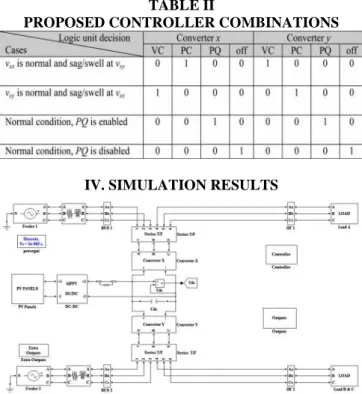
III. OVERALL SYSTEM CONTROLLER Fig. 8 shows the proposed controller for a two-line IVDFC (two feeders are involved, namely, feeder x and feeder y), which is able to manage the power transfer through the dc-link in normal as well as abnormal operating conditions. As a general controller, voltage sag/swell and DF improvement problems are merged into one control circuit. Referring to Fig. 8, each converter may be switched to one of four possible modes (off mode, VC mode, PC mode, or PQ mode). The PCC voltages are continuously monitored by a logic unit that is responsible for choosing the appropriate mode of operation for each converter based on the voltage levels.
Fig. 8 Proposed controller
The following section will show how different modes of operation are handled individually in the proposed controller. A set of scenarios can be envisioned for the
system. The main cases are summarized in Table II and in the following subsections (where the hyphenated condition describes the state of one of the feeders to the left of the hyphen and the other feeder to the right of the hyphen). For all other cases, the converters will be switched to the off position.
A. Normal–Normal (PQ Sharing Mode is disabled)
In this case, the logic unit selects the off positions (see Fig. 8) for both converters.
B. Normal–Normal (PQ Sharing Mode is enabled)
In this case, the logic unit selects the PQ positions (see Fig. 8) for both converters after verifying all constraints that accompany this mode. Based on the DFs of the loads connected to the involved feeders (DFLx and DFLy), the direction of active power flow will be defined. The feeder with a lower load DF will be the sourcing feeder with a positive active power reference, and the other feeder will be the receiving feeder with a negative active power reference. In Fig. 8, the sign of the variable h, which represents the difference between the two DFs, is used to determine the sign of the different reference powers. To maintain a constant dc-link voltage during the PQ sharing mode, the output of the dc link voltage controller, ΔP (which represents the active power needed to regulate the dc link) is added to the reference active power of the sourcing feeder. To achieve that, the two DFs (DFLx, and DFLy) are compared to decide the sourcing and receiving feeders. The comparatoroutput is used to add ΔP to the reference active power of the sourcing feeder only as shown in Fig. 8.
For example, if DFLx is less than DFLy, the comparator outputwill be high; therefore, ΔP will be added to Pex (i.e., P∗x = Pex+ΔP and P∗y =−Pex). The voltage reference of each converter is then determined based on the corresponding active power references (P∗x and P∗y) as given by (9)–(12), where i = x or y
C. Normal–Voltage Sag
If one feeder exhibits voltage sag, the logic unit has to switch its series converter to VC position (see Fig. 8) to regulate the load voltage, and the required power for restoration will be absorbed from the dc link. The converter of the healthy feeder will be switched to its PC position (see Fig. 8) to replenish the dc-link voltage. The needed power to restore the dc link voltage will be the output of the dc voltage controller. This power is used to estimate the corresponding converter reference voltage.
D. Normal–Voltage Swell
the dc-link voltage. The amount of power, which should be absorbed by the healthy feeder, will be the output of the dc voltage controller.
In this paper the proposed system with PV can control the voltage unbalances like voltage sags, swells etc. The displacement factor will be improved by active and reactive power sharing between the feeders by a DC link, which is controlled by PV system. This system creates the importance of renewable systems at distribution sector.
TABLE II
PROPOSED CONTROLLER COMBINATIONS
IV. SIMULATION RESULTS
Fig 9 simulink diagram of proposed IVDFC with PV system
TABLE III SIMULATION DATA
Fig 10 DC voltage of PV system
A. Normal Operating Conditions (PQ Sharing Mode) 1) Case 1: During normal operating conditions, feeder 2 is
feeding an impedance of 10 Ω (40 Ω // 13.33 Ω) with a 0.99
lagging DF (receiving feeder), while feeder 1 is feeding an
impedance of 40 Ω with a 0.8 lagging DF (sourcing feeder).
If it is desired to improve the DF of bus1 to 0.95 (DFa ), the proposed PQ sharing mode is employed. The exchanged active power command (Pex ) is calculated based on (8). For the data given in Table III, the amount of active power needed to increase the DF of the sourcing feeder (feeder 1) from 0.8 lagging to 0.95 lagging is≈544.5 W (3 (220 V × (220/40)A × (0.95−0.8))). On the other hand, the amount of active power needed to decrease the DF of the receiving feeder (feeder 2) from 0.99 lagging to 0.95 lagging is≈580.8 W (3 (220 V × (220/10)A × (0.99−0.95))), i.e., Pex should be the minimum of these two values (544.5, 580.8).
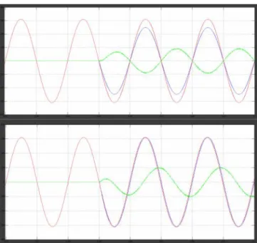
Hence, the controller sets Pex to 544.5 W. This value is applied to the controller at t = 0.05 s. The injected, supply voltage and supply current of buses 1 and 2 are in Fig. 11(a) and (b), respectively. When the PQ sharing mode is applied, the phase difference between the supply voltage and current of bus 1 is decreased, i.e., DF of bus 1 is improved. On the other hand, the phase difference between the supply voltage and current of bus 2 is slightly increased, i.e., its DF is decreased. The DF of each bus before and after applying the PQ sharing mode is shown in Fig. 11(c). The simulation results in this case are summarized in Table IV. Generally, it shows slight variation in DF of bus 2 while the DF of bus1 is improved from 0.8 to 0.95 lagging successfully.
.
TABLE IV
Fig. 11 Per-phase PQ sharing mode simulation results: (a)–
(c) for first case
Fig. 12 Per-phase PQ sharing mode simulation results: (d)–
(f) for the second case
2) Case 2: In this case, load (A) has a lower DF compared to the aforementioned case (0.5 lagging instead of 0.8 lagging). The amount of active power needed to increase the DF of the sourcing feeder from 0.5 lagging to 0.95 lagging is 1633.5 W (3 (220 V × (220/40)A × (0.95−0.5))). On the other hand, the amount of active power needed to decrease the DF of the receiving feeder is not changed (580.8 W), i.e., Pex should be the minimum of these two values (1633.5, 580.8). Hence, the controller sets Pex to 580.8 W. This value is applied to the controller at t = 0.05 s. The injected, supply voltage and supply current of buses 1 and 2 are in Fig. 12(d) and (e), respectively. The DF of each bus before and after applying the PQ sharing mode is shown in Fig. 12(f). The simulation results for this case are also summarized in Table IV. Generally, it shows that the DF of bus 1 is improved from 0.5 to 0.66 lagging; hence, reaching
the desired value was not possible since the DF of the receiving feeder reached its minimum accepted level (DFa )
Fig. 12 Per-phase simulation results for voltage sag case: (a) at feeder 1 and (b) at feeder 2
V. CONCLUSION
This paper proposes a new operational mode for the IDVR to improve the DF of different feeders under normal operation. In this mode, the DF of one of the feeders is improved via active and reactive power exchange (PQ sharing) between feeders through the common dc link is supplied by using solar energy (PV). The same system can also be used under abnormal conditions for voltage sag/swell mitigation. Under PQ sharing mode, the injected voltage in any feeder does not affect its load voltage/current magnitude, however, it affects the DFs of both sourcing and receiving feeders. From the results it can observed that the PQ sharing will be done between the feeders using PV system via common DC link capacitor. In the unbalanced conditions like sags/swells the PV system maintained the system balanced and by maintaing constant DC voltage at the common DC link capacitor. The proposed mode is highly beneficial if the active power rating of the receiving feeder is higher than the sourcing feeder. The DF of the sourcing feeder increases while the DF of the receiving feeder decreases. When applying the proposed concept, some constraints should be satisfied to maintain the DF of both sourcing and receiving feeders within acceptable limits imposed by the utility companies. These operational constraints have been identified and considered. In this case, the DF of the sourcing feeder will have a notable improvement with only a slight variation in DF of the receiving feeder.
VI. ACKNOWLEDGMENT
REFERENCES
[1] S. A. Qureshi and N. Aslam, “Efficient power factor
improvement technique and energy conservation of power
system,”Int. Conf. Energy Manage. Power Del., vol. 2, pp. 749–752, Nov. 21–23, 1995.
[2] J. J.Grainger and S. H. Lee, “Optimum size and location
of shunt capacitors for reduction of losses on distribution
feeders,”IEEE Trans. Power App. Syst., vol. PAS-100, no. 3, pp. 1105–1118, Mar. 1981.
[3] S. M. Kannan, P. Renuga, and A. R. Grace, “Application
of fuzzy logic and particle swarm optimization for reactive power compensation of radial distribution systems,” J. Electr. Syst., 6-3, vol. 6, no. 3, pp. 407–425, 2010.
[4] L. Ramesh, S. P. Chowdhury, S. Chowdhury, A. A. Natarajan, andC. T. Gaunt, “Minimization of power loss in distribution networks bydifferent techniques,”Int. J. Electr. Power Energy Syst. Eng., vol. 3, no. 9, pp. 521–527, 2009.
[5] T. P.Wagner, A. Y. Chikhani, and R. Hackam, “Feeder
reconfiguration for loss reduction: An application of
distribution automation,” IEEE Trans. Power Del., vol. 6, no. 4, pp. 1922–1933, Oct. 1991.
[6] A. Luo, Z. Shuai,W. Zhu, and Z. J. Shen, “Combined
system for harmonic suppression and reactive power
compensation,”IEEE Trans. Ind. Electr., vol. 56, no. 2, pp. 418–428, Feb. 2009.
[7] S. B. Karanki, N. Geddada, M. K. Mishra, and B. K.
Kumar, “A DSTATCOMtopology with reduced DC link voltage rating for load compensationwith nonstiff source,”
IEEE Trans. Power Electr., vol. 27, no. 3, pp. 1201–1211, Mar. 2012.
[8] K. Sano and M. Takasaki, “A transformerless D -STATCOM based on a multivoltage cascade converter
requiring no DC sources,” IEEE Trans. Power Electr., vol. 27, no. 6, pp. 2783–2795, Jun. 2012.
[9] B. Singh and S. R. Arya, “Adaptive theory-based improved linear sinusoidal tracer control algorithm for
DSTATCOM,”IEEE Trans. Power Electron., vol. 28, no. 8, pp. 3768–3778, Aug. 2013.
[10] S. Du, J. Liu, J. Lin, and Y. He, “A novel DC voltage
control method for STATCOM based on hybrid multilevel H-bridge converter,” IEEE Trans. Power Electr., vol. 28, no. 1, pp. 101–111, Jan. 2013.
[11] B. Singh and S. R. Arya, “Adaptive theory-based improved linear sinusoidal tracer control algorithm for
DSTATCOM,” IEEE Trans. Power Electr., vol. 28, no. 8, pp. 3768–3778, Aug. 2013.
[12] R. S. Kemerer and L. E. Berkebile, “Directly connected
static VAR compensation in distribution system
applications,” IEEE Trans. Ind. Appl., vol. 35, no. 1, pp. 176–182, Jan./Feb. 1999.
[13] C. Wessels, F. Gebhardt, and F. W. Fuchs, “Fault ride -through of a DFIG wind turbine using a dynamic voltage restorer during symmetrical and asymmetrical grid faults,”
IEEE Trans. Power Electr., vol. 26, no. 3, pp. 807–815, Mar. 2011.
[14] A. Y. Goharrizi, S. H. Hosseini, M. Sabahi, and G. B. Gharehpetian, “Three-phase HFL-DVR with independently
controlled phases,”IEEE Trans. Power Electr., vol. 27, no. 4, pp. 1706–1718, Apr. 2012.
[15] D. Ramirez, S. Martinez, C. A. Platero, F. Blazquez, and R. M. de Castro, “Low-voltage ride-through capability for wind generators based on dynamic voltage restorers,”
IEEE Trans. on Energy Convers., vol. 26, no. 1, pp. 195–
203, Mar. 2011.
[16] B. Bae, J. Lee, J. Jeong, and B. Han, “Line-interactive single-phase dynamic voltage restorer with novel sag
detection algorithm,”IEEE Trans. Power Del., vol. 25, no. 4, pp. 2702–2709, Oct. 2010.
[17] F. B. Ajaei, S. Afsharnia, A. Kahrobaeian, and S.
Farhangi, “A fast and effective control scheme for the