A nanocomposite ultraviolet photodetector based
on interfacial trap-controlled charge injection
Fawen Guo, Bin Yang, Yongbo Yuan, Zhengguo Xiao, Qingfeng Dong, Yu Bi and Jinsong Huang
*
Ultraviolet photodetectors have applications in fields such as medicine, communications and defence1, and are typically
made from single-crystalline silicon, silicon carbide or gallium nitride p–n junction photodiodes. However, such inorganic photodetectors are unsuitable for certain applications because of their high cost and low responsivity (<0.2 A W21)2.
Solution-processed photodetectors based on organic materials and/or nanomaterials could be significantly cheaper to manu-facture, but their performance so far has been limited2–7.
Here, we show that a solution-processed ultraviolet photo-detector with a nanocomposite active layer composed of ZnO nanoparticles blended with semiconducting polymers can significantly outperform inorganic photodetectors. As a result of interfacial trap-controlled charge injection, the photodetec-tor transitions from a photodiode with a rectifying Schottky contact in the dark, to a photoconductor with an ohmic contact under illumination, and therefore combines the low dark current of a photodiode and the high responsivity of a photoconductor (∼721–1,001 A W21). Under a bias of<10 V, our device provides a detectivity of 3.431015Jones at 360 nm at room temperature, which is two to three orders of magnitude higher than that of existing inorganic semiconductor ultraviolet photodetectors.
The use of solution-processed thin films of colloidal inorganic semiconductor nanoparticles or colloidal quantum dots as photo-conductors has been a critical step in the quest to fabricate low-cost photodetectors. Several types of nanomaterials, including PbS colloidal quantum dots and ZnO nanoparticles, have been used to measure different response spectra ranging from the near-infrared to the ultraviolet2–4,6,8. These photodetectors demonstrate
remark-ably high responsivities—greater than 1,000 A W21 in the near-infrared range3,6 and 61 A W21
in the ultraviolet2. However, the
lateral structure adopted in these photoconductive photodetectors inevitably leads to large driving voltages and slow responses. A large lateral electrode spacing (.5 mm) is required to increase the shunt resistance and reduce the dark current, so, to maintain high gain, these photodetectors need a very high driving voltage of 100 V, which cannot be provided by commercially available thin-film transistors2,3,7. The response speed of lateral-structure
photoconductive photodetectors is also sacrificed to maintain this high gain. Gain is determined by the ratio of the lifetime of the free charge and the transit time9. A large electrode spacing is
needed to allow more light to be absorbed, both for high gain and to reduce the dark current, but this increases the transit time of the charges across the electrodes. A long trapping time (on the scale of minutes) is therefore needed, which inevitably limits the applications of these photodetectors2,3,6.
A vertical-structure photoconductive photodetector, with its much smaller electrode spacing, has a much shorter carrier transit length, therefore providing high gain as well as a quick response. A photoactive layer thickness of 500 nm is generally thick
enough to absorb most of the ultraviolet radiation, as a result of the high absorption coefficient of many types of nanoparticles in the ultraviolet range10. One challenge in making a vertical-structure
photoconductive photodetector with such a thin absorber film is dealing with the large dark current injected from its much larger electrode contact area than in lateral structures. Ohmic contact with at least one of the electrodes is required to take advantage of the high gain of the photoconductors9. However, the large charge
injection, combined with the relatively smaller shunt resistance (due to the much shorter charge transit length than in the lateral structure), will result in a large dark current, which can ruin the detectivity of the photodetector11. The large dark current problem
is exacerbated when using non-dense nanoparticle films, which are susceptible to the penetration of metal atoms by diffusion during metallization and subsequent thermal treatment.
We have developed a highly sensitive ultraviolet photodetector with a vertical device structure combining the gain of a photocon-ductor and the low noise of a diode. The active-layer materials are nanocomposites composed of ZnO nanoparticles blended with semiconducting polymers. ZnO is emerging as a potential alternative to GaN or SiC as an ultraviolet absorber due to its wide bandgap of 3.4 eV, low-cost material and variable synthetic strategies2,12–19. Our nanocomposite photodetectors were
fabricated using a low-cost spin-coating process, which is compatible with complementary metal–oxide–semiconductor (CMOS) readout circuits4.
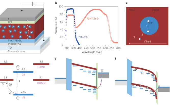
The structure and operating principle of our photodetector are presented in Fig. 1. The simple device structure comprises a polymer:ZnO nanocomposite layer sandwiched between a transpar-ent indium tin oxide (ITO) anode and an aluminium cathode (for chemical structures of the materials see Supplementary Fig. S1). This device structure is essentially the same as those of polymer:na-noparticle hybrid solar cells20–22or bistable memories23, except that
the nanoparticles work as charge traps in our photodetector instead of as charge conductors (as is the case in hybrid solar cells). Two types of hole-conducting semiconducting polymers were used to obtain different response spectra (Fig. 1b): poly-3(hexylthiophene) (P3HT, optical bandgap of 1.9 eV) for UV–vis detection and poly-vinylcarbazole (PVK, bandgap of 3.5 eV) for ultraviolet detection. PVK is used because of its reasonably high hole mobility and very high bandgap, although it is not a conjugated polymer. To minimize the dark current, a thin layer of 4,4′ -bis[(p-trichlorosilylpropylphe-nyl)phenylamino]-biphenyl (TPD-Si2) and PVK blend was inserted
between poly(3,4-ethylenedioxythiophene) poly(styrenesulphonate) (PEDOT:PSS) and the nanocomposite layer as an electron-blocking/hole-conducting layer. This material blend combines the hole-injection and hole-transport capabilities of TPD-Si224 with
the electron-blocking capability of PVK and has been shown to reduce the dark current by two to three orders of magnitude in our devices. The hole-transport layer was crosslinked by annealing TPD-Si2 in air so that the photoactive layer coating step that
follows would not wash it away. Similarly, a hole-blocking/ electron-conducting layer—2,9-dimethyl-4,7-diphenyl-1,10-phenanthroline (BCP)—was also deposited by thermal evaporation on the cathode side.
The hybrid photodetector works as follows. First, both the nano-particles and polymers absorb incident photons and generate Frenkel excitons (Fig. 1c, 1). The Frenkel excitons then diffuse to the polymer/nanoparticles interface and the electrons transfer from the nanoparticles and semiconducting polymer, as shown in the energy diagram (Fig. 1d, 2). Holes are transported in the semi-conducting polymer under the applied reverse bias/electric field, while the electrons remain trapped in the nanoparticles due to the lack of a percolation network for electrons and the strong quantum confinement effect in nanoparticles (Fig. 1c, 3). The strong electron trapping effect is demonstrated by the very small electron current in the electron-only devices, which is three to four orders of magnitude lower than the hole current in hole-only devices using the same nanocomposite layers as the carrier transport layer (Supplementary Fig. S2). The electron trapping effect of the ZnO nanoparticles was also directly observed by electrostatic force microscopy (EFM) (Supplementary Fig. S3). In the absence of illu-mination, the dark current is small because of the very large charge injection barrier (.0.6 eV) under reverse bias, as illustrated in Fig. 1e. Under illumination, the trapped electrons quickly shift the lowest unoccupied molecular orbital (LUMO) of the polymer down-wards and align the Fermi energy of the nanocomposite with that of the cathode. The electron traps are predominantly located close to the cathode because of the formation of vertical phase separation in the nanocomposite, with ZnO nanoparticles segregated to the cathode side, as observed by cross-sectional scanning electron microscopy (SEM; Supplementary Fig. S4). This phase separation (both lateral and vertical) has been observed widely in P3HT:ZnO nanocomposites and was purposely promoted by the slow drying
of the film taking advantage of the different surface affinity of ZnO and P3HT for the substrate20,25–27. The hole-injection barrier
on the cathode side becomes so thin that the holes can easily tunnel through it with a small reverse bias (Fig. 1f ). Accordingly, the nanocomposite/aluminium interface acts as a photon-address-able optoelectronics ‘valve’ for hole injection, and incident photons can switch on this ‘valve’. The average energy barrier change,DF, is a linear function of trapped electron densitynt, and the injection
current follows an exponential relationship with the energy barrier change according to the Richardson–Dushman equation:
J/exp −DF kT
/exp nt kT
wherekis the Boltzmann constant andTis the temperature. The gain of a photodetector is the ratio of the measured photocurrent (carriers) and the number of incident photons. If the injected hole number exceeds the absorbed photon number, there is gain as a result of the exponential dependence of the injected holes on incident photons.
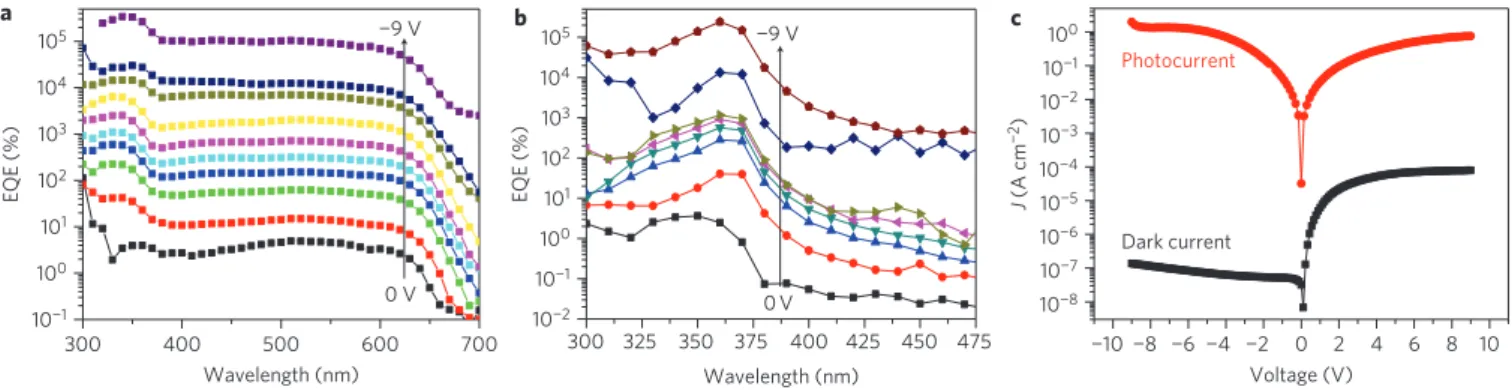
To characterize the wavelength-dependent gain of the photode-tectors, external quantum efficiency (EQE) versus wavelength was measured using an incident photon-to-current efficiency (IPCE) system at different reverse biases (Fig. 2a,b). The EQE curves also agree with the absorption curves of the nanocomposites. EQE values exceed 100% at a bias of 23 V for PVK:ZnO devices and
21 V for P3HT:ZnO devices, and increase quickly with increasing negative bias, especially at reverse biases above 28 V. The rapid increase of EQE is consistent with the rapid increase of photocur-rent, as shown in Fig. 2c. For a bias of29 V (the highest voltage output of our light bias amplifier) at 360 nm, the peak EQE values are 245,300% and 340,600% for the PVK:ZnO and a
d e f
b c
300 350 400 450 500 550 600 650 700 0
20 40 60 80 100
Absorption (%)
Wavelength (nm) P3HT:ZnO
PVK:ZnO
P3HT
− NP
Ligand
E field 1
2 3
3
1
LUMO
CB
VB
HOMO
− 3.2
5.1
2
4.3
7.65
3.2
5.1
X −
−
− −
− −
− −
− −
−
−
− − − −
+
+
+ +
+
+
+ +
+ −
− −
− − −
+
+ +
+ +
+ AI
BCP
PVK:TPD-Si2 PEDOT:PSS ITO
Glass substrate −
P3HT:ZnO devices, respectively. The corresponding responsivity (R in A W21)—that is, the ratio of photocurrent to intensity of incident light—can be calculated from the EQE using
R=EQE/hn
wherehnis the energy of the incident photon in electronvolts. The peak responsivities at an illumination light intensity of 1.25mW cm22
are 721 A W21
for the PVK:ZnO device and 1,001 A W21 for the P3HT:ZnO device at 360 nm; these values are more than three orders of magnitude larger than those of com-mercial GaN or SiC photodetectors (,0.2 A W21). Indeed, they are the highest reported responsivities of all types of solid-state ultra-violet photodetectors2,5,6.
Our nanocomposite photodetector devices show a transition in operation from a photodiode in the dark with a rectifying Schottky contact, to a photoconductor under illumination with an ohmic contact, as shown by the dark current and photocurrent traces in Fig. 2c. The combination of the low dark current of the photodiode and large gain of the photoconductor is expected to yield a new type of photodetector with high sensitivity. The figure of merit for a photodetector is the specific detectivity that character-izes the capability of a photodetector to detect the weakest light signal9. In addition to responsivity, the other factor that limits the
specific detectivity of a photodetector is the noise current. The dark current of our device is as low as 6.8 nA at29 V because of the blocking contact both at the anode and cathode sides under dark conditions (Fig. 2c), which provides a very low shot noise. To include other possible noise, such as flicker noise and thermal noise, the total noise current of the photodetector was directly measured with an SR830 lock-in amplifier under different con-ditions of dark current density and frequency3,4. As shown in
Fig. 3a,b, the measured total noise current was found to be domi-nated by the shot noise within the frequency range 1 Hz to 5 kHz. The specific detectivities (D*) of a photodetector are given by7,9
D∗=( )AB
1/2
NEP cm Hz
1/2
W−1or Jones
NEP=i
2 n
1/2
R ( )W
whereA is the device area,Bis the bandwidth, NEP is the noise equivalent power,i2
n 1/2
is the measured noise current, andRis the responsivity. The detectivities of our nanocomposite photodetector were calculated at different wavelengths with the measured noise current and responsivity at29 V bias, and the results are plotted in Fig. 3c. At an illumination light intensity of 1.25mW cm22,
the specific detectivities at 360 nm were 3.4×10¹⁵Jones for
PVK:ZnO devices and 2.5×10¹⁴Jones for P3HT:ZnO devices. The specific detectivities in the ultraviolet range were two to three orders of magnitude larger than those of silicon and GaN ultraviolet photodetectors. The specific detectivity of a P3HT:ZnO device within the visible light range was also more than ten times better than that of silicon photodetectors.
Another important parameter of photodetectors is their response speed. The temporal response of our nanocomposite photodetector was characterized using a chopper-generated short light pulse. Figure 4 shows the transient photocurrent of the P3HT:ZnO device measured under a bias of 29 V at a light intensity of 1mW cm22
. The transient response result shows a rise time (output signal changing from 10% to 90% of the peak output value) of 25ms, which was limited by the rising edge of the light pulse from the optical chopper. The decay of the photocurrent after switching off the ultraviolet pulse has a fast component of 142ms and a slow component of 558ms, which indicates the exist-ence of two channels for the recombination of holes. The response speed is among the highest reported in any nanoparticle- or col-loidal quantum dot-based photodetector2–4,6,8. The 3 dB bandwidth
is 9.4 kHz. The devices provide an improvement by a factor of over 1×10⁵ in gain–bandwidth product in solution-processed ZnO ultraviolet photodetection relative to previous reports2. The
mul-tiple-exponential decay time can arise from the existence of electron traps with different trap depths due to the non-uniform nature of ZnO nanoparticles or aggregates in the present hybrid devices. Deeper traps have longer charge release times and thus result in a slower device response speed. It should be mentioned that the photodetector response speed is related to trap occupancy, which depends on light intensity. At lower light intensity, the photocurrent decay is expected to be dominated by the slower process of 558ms, because deeper traps are easier to be filled. The response speed of hybrid devices at a light intensity of ,1mW cm22 was not measured, because the lower light intensity could not provide suffi-cient signal for the present measurement system. Increasing the response speed at lower light levels by improving the uniformity of the ZnO nanoparticles is still under investigation. The photocon-ductive gain is the ratio between hole recombination time, or device switch-off time, and the transit time during which holes sweep through the nanocomposite film to the ITO. The gain of the P3HT:ZnO device calculated from the measured hole mobility and hole recombination time is 3,798, which is very close to the gain measured by IPCE (see Supplementary Information).
A photodetector needs to have a large linear dynamic range so as to measure both strong and weak light. The linear dynamic range of the nanocomposite photodetector was also characterized by measuring the photocurrent at a fixed frequency of 35 Hz but with varied light intensity from 1×10²¹W cm22to 1×10212W cm22.
a b c
300 400 500 600 700
10−1 100 101 102 103 104 105
10−1
10−2 100 101 102 103 104 105
−9 V −9 V
EQE (%) EQE (%)
Wavelength (nm) 0 V
300 325 350 375 400 425 450 475
Wavelength (nm)
−10 −8 −6 −4 −2 0 2 4 6 8 10 10−8
10−7 10−6 10−5 10−4 10−3 10−2 10−1 100
Dark current
J
(A cm
−2
)
Voltage (V) Photocurrent
0 V
As shown in Fig. 5, the PVK:ZnO photodetector shows a linear response within the incident light intensity range from 1×10²¹W cm22to 1×1029W cm22, corresponding to a linear dynamic range of 80 dB. This is among the highest reported linear dynamic ranges for both inorganic and organic ultraviolet photodetectors. The responsivity remains almost constant in this light intensity range, despite a slight (10%) drop at high light
levels (Fig. 5, inset). This slight sublinear response at high light intensities is possibly caused by electron trapping saturation and/or limitation of hole mobility in the nanocomposite layers. The device begins to lose its linearity when the incident light inten-sity is below 1×1029W cm22. The responsivity drops to 52 A W21 and the specific detectivity accordingly drops to 2.45×10¹⁴Jones at a light intensity of 1.25×10212W cm22. The sublinearity and reduced detectivity at low light levels is a disadvantage, because high gain at low light intensity is desired for weak light detection; however, it can be improved by tuning the morphology of the nanocomposite layer. In principle, we expect a constant responsivity down to the lowest detectable inci-dent light level (NEP) if the automatic transition from the Schottky junction to ohmic contact occurs at such a low incident light level. This is possible, because the incident photons can cause band bending in the local environment surrounding the light-absorbing ZnO nanoparticles, which induces strong local hole injection. However, the degree of local band bending varies
10−12
10−13 10−11 10−9 10−7 10−5 10−3 10−1 10−10
10−8 10−6 10−4 10−2 100 102
J
(A cm
−2
)
Irradiance (W cm−2)
10−1310−1110−910−710−510−3 10−1 101
102 103
R
(A W
−1)
Irradiance (W cm−2)
Figure 5 |Dynamic range of the PVK:ZnO photodetector.The device shows a linear response within the incident light intensity range, which corresponds to a linear dynamic range of 80 dB. Inset: responsivities under different illumination intensities.
0.0 0.5 1.0 1.5 2.0
0 1
Photocurrent (a.u)
Time (ms)
τ1 = 142μs
τ2 = 558μs
Figure 4 |Transient photocurrent of the P3HT:ZnO device.Photocurrent is measured under a bias of29 V with a light intensity of 1mW cm22, and an optical chopper is used to provide short light pulses. After switching off the ultraviolet pulse, the decay of the photocurrent has a fast component of 142ms and a slow component of 558ms, which indicates that there are two channels for the recombination of holes.
a
b
c
60 80 100 120 140
10−2
10−1
10−2
10−3
1015
1014
1013 10−1 100
100 101 102 103 10−1
100 101
Noise current (pA Hz
−1/2
)
Noise current (pA Hz
−1/2
)
Dark current (nA) Shot noise limit
Thermal noise limit
Noise current (pA Hz
−1/2
)
Noise current (pA Hz
−1/2
)
Frequency (Hz)
100 101 102 103 Frequency (Hz) P3HT:ZnO
3 4 5 6 7 8
10−2 10−1 100 101
Dark current (nA) Shot noise limit
Thermal noise limit PVK:ZnO
300 600 900
D
* (Jones)
Wavelength (nm)
PVK:ZnO
P3HT:ZnO
Silicon
GaN
with the morphology of the nanocomposite layer. If there is an aggregation of ZnO nanoparticles, which is very likely to occur in our material system, the local average trapped electron density will be reduced and the induced charge injection will be weakened. In addition, there are still many ZnO nanoparticles located in the middle of the nanocomposite layers or at the anode side, despite the higher concentration of ZnO nanoparticles at the cathode side due to the TPD-Si2 interface-induced vertical phase separation.
Light absorption by these ZnO nanoparticles located far away from the cathode will not induce as much of a Schottky junction-narrowing effect as those close to the cathode side. This non-ideal morphology might increase the lowest light intensity detectable by the nanocomposite photodetector. The influence of morphology on the lowest detectable light intensity is still under investigation, and we expect to see a lower limit of detectable light intensity and a better linear response by pushing more ZnO nanoparticles closer to the cathode side.
We have reported a new type of hybrid photodetector that has a Schottky contact in the dark and an ohmic contact under illumina-tion, enabled by interfacial trap-controlled charge injection. Its specific detectivity of 3.4×10¹⁵Jones is tens to hundreds of times better than that of inorganic semiconductor photodetectors. It should be noted that ZnO nanomaterial-based ultraviolet photode-tectors have been extensively explored over the past decade, with most effort focusing on single nanowires because of their quick response, which arises from their large carrier mobility2,12–19.
However, for several reasons, these devices have not shown comparable performance or any advantage over inorganic ultraviolet photodetectors. First, the photodetectors have been constructed from a single nanowire and have not been scalable to large areas using current synthesis techniques. Second, the ZnO nanowires are directly connected to two electrodes, leading to high dark current. In contrast to these earlier photodetectors, which were constructed with material systems similar to ours, our ultraviolet photodetectors can be made at low cost, and can be scaled up easily to large areas. They also have very high gain and very low dark current because of the absence of ohmic contact in the dark, and can respond quickly. Our nanocomposite photo-detectors have great potential for replacing inorganic ultraviolet photodetectors and for opening avenues to new applications.
Methods
ZnO nanoparticles were prepared using a hydrolysis method in methanol with some modifications. EFM was used to characterize the topography and electron trap distribution in the nanocomposite films. The cross-sectional morphology of the P3HT:ZnO nanoparticle nanocomposite was measured by SEM. EQE was measured with a Newport QE measurement kit by focusing a monochromatic beam of light onto the devices. For the transient response measurement, an optical chopper was used to provide the light pulse, and an oscilloscope (LeCroy WaveRunner) was used to record the voltage variation of the resistor. The absorption spectra of the photoactive layers were measured with a PerkinElmer Lambda 900 spectrometer. Film thickness was measured with an AMBIOS XP-2 stylus profilometer. Noise current was directly measured with a lock-in amplifier SR830.
Received 10 May 2012; accepted 24 September 2012; published online 11 November 2012
References
1. Li, W. D. & Chou, S. Y. Solar-blind deep-UV band-pass filter (250–350 nm) consisting of a metal nano-grid fabricated by nanoimprint lithography. Opt. Express18,931–937 (2010).
2. Jin, Y. Z., Wang, J. P., Sun, B. Q., Blakesley, J. C. & Greenham, N. C. Solution-processed ultraviolet photodetedtors based on colloidal ZnO nanoparticles. Nano Lett.8,1649–1653 (2008).
3. Konstantatos, G.et al. Ultrasensitive solution-cast quantum dot photodetectors. Nature442,180–183 (2006).
4. Chen, H., Lo, M., Yang, G., Monbouquette, H. & Yang, Y. Nanoparticle-assisted high photoconductive gain in composites of polymer and fullerene.Nature Nanotech.3,543–547 (2008).
5. Sukhovatkin, V., Hinds, S., Brzozowski, L. & Sargent, E. H. Colloidal quantum-dot photodetectors exploiting multiexciton generation.Science 324,1542–1544 (2009).
6. Konstantatos, G. & Sargent, E. H. Nanostructured materials for photon detection.Nature Nanotech.5,391–400 (2010).
7. Gong, X.et al. High-detectivity polymer photodetectors with spectral response from 300 nm to 1450 nm.Science325,1665–1667 (2009).
8. Arnold, M. S.et al. Broad spectral response using carbon nanotube/organic semiconductor/C60 photodetectors.Nano Lett.9,3354–3358 (2009). 9. Liu, J-M.Photonic Devices960–986 (Cambridge Univ. Press, 2005). 10. Yoshikawa, H. & Adachi, S. Optical constants of ZnO.Jpn. J. Appl. Phys.36,
6237–6243 (1997).
11. Redington, R. W. Maximum performance of high-resistivity photoconductors. J. Appl. Phys.29,189–193 (1958).
12. Chen, K. J., Hung, F. Y., Chang, S. J. & Young, S. J. Optoelectronic characteristics of UV photodetector based on ZnO nanowire thin films.J. Alloy Comp.479, 674–677 (2009).
13. Li, Y., Della Valle, F., Simonnet, M., Yamada, I. & Delaunay, J-J. High-performance UV detector made of ultra-long ZnO bridging nanowires. Nanotechnology20,045501 (2009).
14. Kind, H., Yan, H. Q., Messer, B., Law, M. & Yang, P. D. Nanowire ultraviolet photodetectors and optical switches.Adv. Mater.14,158–160 (2002). 15. Soci, C.et al. ZnO nanowire UV photodetectors with high internal gain.
Nano Lett.7,1003–1009 (2007).
16. Liang, S.et al. ZnO Schottky ultraviolet photodetectors.J. Cryst. Growth225, 110–113 (2001).
17. Lao, C. S.et al. Giant enhancement in UV response of ZnO nanobelts by polymer surface-functionalization.J. Am. Chem. Soc.129,12096–12097 (2007). 18. Das, S. N.et al. ZnO single nanowire-based UV detectors.Appl. Phys. Lett.
97,022103 (2010).
19. Basak, D., Amin, G., Mallik, B., Paul, G. K. & Sen, S. K. Photoconductive UV detectors on sol–gel-synthesized ZnO films.J. Cryst. Growth256,73–77 (2003). 20. Oosterhout, S. D.et al. The effect of three-dimensional morphology on the
efficiency of hybrid polymer solar cells.Nature Mater.8,818–824 (2009). 21. Sun, B. Q., Marx, E. & Greenham, N. C. Photovoltaic devices using
blends of branched CdSe nanoparticles and conjugated polymers. Nano Lett.3,961–963 (2003).
22. Huynh, W. U., Dittmer, J. J. & Alivisatos, A. P. Hybrid nanorod–polymer solar cells.Science295,2425–2427 (2002).
23. Verbakel, F., Meskers, S. C. J. & Janssen, R. A. J. Electronic memory effects in diodes from a zinc oxide nanoparticle–polystyrene hybrid material. Appl. Phys. Lett.89,102103 (2006).
24. Huang, Q.et al. Covalently bound hole-injecting nanostructures. Systematics of molecular architecture, thickness, saturation, and electron-blocking characteristics on organic light-emitting diode luminance, turn-on voltage, and quantum efficiency.J. Am. Chem. Soc.127,10227–10242 (2005). 25. Beek, W. J. E., Wienk, M. M., Kemerink, M., Yang, X. N. & Janssen, R. A. J.
Hybrid zinc oxide conjugated polymer bulk heterojunction solar cells.J. Phys. Chem. B109,9505–9516 (2005).
26. Campoy-Quiles, M.et al. Morphology evolution via self-organization and lateral and vertical diffusion in polymer: fullerene solar cell blends.Nature Mater.7, 158–164 (2008).
27. Baoquan, S., Snaith, H. J., Dhoot, A. S., Westenhoff, S. & Greenham, N. C. Vertically segregated hybrid blends for photovoltaic devices with improved efficiency.J. Appl. Phys.97,014914 (2005).
Acknowledgements
This work was supported by the Office of Naval Research (ONR, grant no. N000141210556), a Defense Threat Reduction Agency (DTRA) Young Investigator Award (HDTRA1-10-1-0098) and the University of Nebraska–Lincoln.
Author contributions
J.H. conceived the idea. J.H. and F.G. designed the experiments and analysed the data. F.G. carried out the fabrication of devices, measurements and data analysis. Y.B., B.Y. and Q.D. synthesized ZnO nanoparticles. B.Y. and Z.X. fabricated the single carrier devices. J.H. and F.G. wrote the manuscript.
Additional information
Supplementary information is available in the online version of the paper. Reprints and permission information is available online at http://www.nature.com/reprints. Correspondence and requests for materials should be addressed to J.H.