This is information on a product in full production.
July 2015 DocID17285 Rev 5 1/18
STLQ015
150 mA, ultra low quiescent current linear voltage regulator
Datasheet
-
production dataFeatures
• Input voltage from 1.5 to 5.5 V
• Very low quiescent current: – 1.0 µA (typ.) at no load – 1.4 µA (typ.) at 150 mA load – 1 nA (typ.) in OFF mode
– 200 nA max. in OFF mode at 125 °C
• Output voltage tolerance: ± 2% at 25 °C
• 150 mA guaranteed output current
• Wide range of output voltages: 0.8 V to 3.3 V in 100 mV steps
• Logic-controlled electronic shutdown
• Compatible with ceramic capacitor (COUT= 1 µF)
• Internal current and thermal limit
• Temperature range: from -40 °C to 125 °C
Description
The STLQ015 provides 150 mA of maximum current with an input voltage range from 1.5 V to 5.5 V and a typical dropout voltage of 112 mV. The key feature of this device is its quiescent current, which is just 1.4 µA at maximum output current. The device is stable with a ceramic capacitor on the output. It offers very low quiescent current and extends battery-life of applications requiring very long standby time. The enable logic control function puts the STLQ015 in shutdown mode, reducing total current
consumption to 1 nA. The device also includes short-circuit constant-current limiting and thermal protection. Typical applications are: portable and battery-powered systems, electronic sensors and microcontroller power supply.
Application
• Mobile phones• Digital still cameras (DSC)
• Battery-powered equipment
• Portable media players SOT23-5L
Contents STLQ015
Contents
1
Block diagram . . . 4
2
Pin configuration and description . . . 5
3
Typical application . . . 6
4
Maximum ratings . . . 7
5
Electrical characteristics . . . 8
6
Typical performance characteristics . . . 10
7
Package information . . . 13
7.1
Packaging mechanical data . . . 15
8
Order code . . . 16
DocID17285 Rev 5 3/18
STLQ015 List of figures
18
List of figures
Figure 1. Device block diagram . . . 4
Figure 2. Pin configuration (top view) . . . 5
Figure 3. Typical application circuit . . . 6
Figure 4. Output voltage vs. temperature . . . 10
Figure 5. Output voltage vs. input voltage (VOUT= 0.8 V) . . . 10
Figure 6. Output voltage vs. input voltage (VOUT= 3.3 V) . . . 10
Figure 7. Dropout voltage vs. temperature . . . 10
Figure 8. Dropout voltage vs. output current . . . 11
Figure 9. Quiescent current vs. temperature . . . 11
Figure 10. Supply voltage rejection vs. frequency . . . 11
Figure 11. Supply voltage rejection vs. IOUT . . . 11
Figure 12. Quiescent current vs. input voltage . . . 11
Figure 13. Quiescent current vs. output current. . . 11
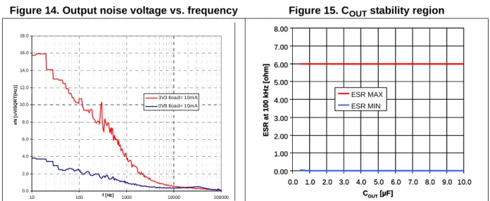
Figure 14. Output noise voltage vs. frequency . . . 12
Figure 15. COUT stability region . . . 12
Figure 16. Start-up transient . . . 12
Figure 17. Enable transient . . . 12
Figure 18. SOT23-5L recommended footprint (dimensions in mm) . . . 14
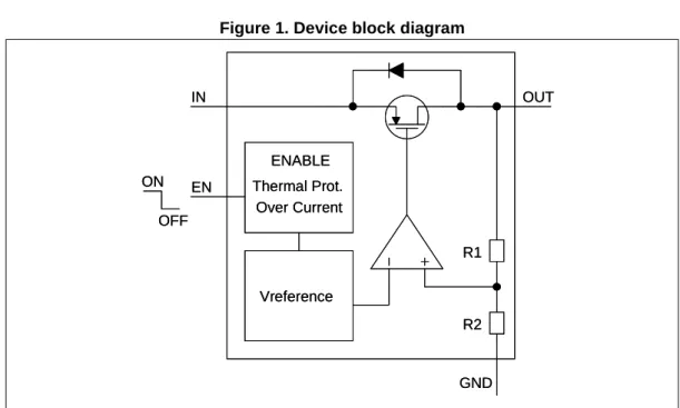
Block diagram STLQ015
1 Block
diagram
Figure 1. Device block diagram
ENABLE Thermal Prot.
Over Current EN
OUT IN
GND R1
R2 Vreference
ON OFF
ENABLE Thermal Prot.
Over Current EN
OUT IN
GND R1
R2 Vreference
ON OFF
DocID17285 Rev 5 5/18
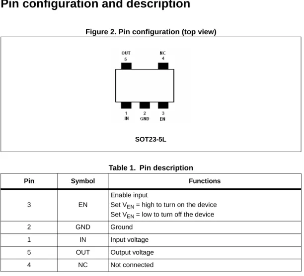
STLQ015 Pin configuration and description
18
2
Pin configuration and description
Figure 2. Pin configuration (top view)
Table 1. Pin description
Pin Symbol Functions
3 EN
Enable input
Set VEN = high to turn on the device Set VEN = low to turn off the device
2 GND Ground
1 IN Input voltage
5 OUT Output voltage
4 NC Not connected
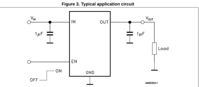
Typical application STLQ015
3 Typical
application
Figure 3. Typical application circuit
DocID17285 Rev 5 7/18
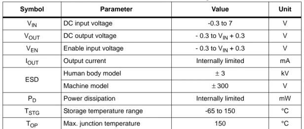
STLQ015 Maximum ratings
18
4 Maximum
ratings
Note: Absolute maximum ratings are those values beyond which damage to the device may occur.
Functional operation under these conditions is not implied. All values are referred to GND.
Table 2. Absolute maximum ratings
Symbol Parameter Value Unit
VIN DC input voltage -0.3 to 7 V
VOUT DC output voltage - 0.3 to VIN + 0.3 V
VEN Enable input voltage - 0.3 to VIN + 0.3 V
IOUT Output current Internally limited mA
ESD Human body model ±3 kV
Machine model ± 300 V
PD Power dissipation Internally limited mW
TSTG Storage temperature range -65 to 150 °C
TOP Max. junction temperature 150 °C
Table 3. Thermal data
Symbol Parameter Value Unit
RthJA Thermal resistance junction-ambient 255 °C/W
Electrical characteristics STLQ015
5 Electrical
characteristics
TJ = 25 °C, VIN = VOUT(NOM) + 1 V, CIN = COUT = 1 µF, IOUT = 1 mA, VEN = VIN, unless otherwise specified.
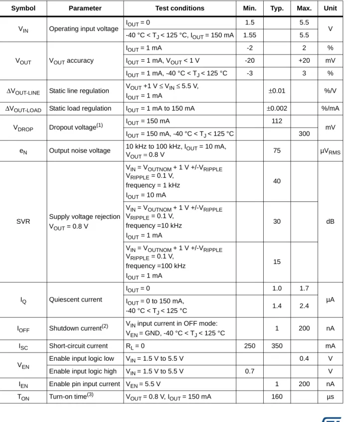
Table 4. Electrical characteristics
Symbol Parameter Test conditions Min. Typ. Max. Unit
VIN Operating input voltage IOUT = 0 1.5 5.5 V
-40 °C < TJ < 125 °C, IOUT = 150 mA 1.55 5.5
VOUT VOUT accuracy
IOUT = 1 mA -2 2 %
IOUT = 1 mA, VOUT < 1 V -20 +20 mV IOUT = 1 mA, -40 °C < TJ < 125 °C -3 3 %
ΔVOUT-LINE Static line regulation VOUT +1 V ≤ VIN≤ 5.5 V,
IOUT = 1 mA ±0.01 %/V
ΔVOUT-LOAD Static load regulation IOUT = 1 mA to 150 mA ±0.002 %/mA
VDROP Dropout voltage(1) IOUT = 150 mA 112 mV
IOUT = 150 mA, -40 °C < TJ < 125 °C 300 eN Output noise voltage 10 kHz to 100 kHz, IOUT = 10 mA,
VOUT= 0.8 V 75 µVRMS
SVR Supply voltage rejection VOUT = 0.8 V
VIN = VOUTNOM + 1 V +/-VRIPPLE VRIPPLE = 0.1 V,
frequency = 1 kHz IOUT = 10 mA
40
dB VIN = VOUTNOM + 1 V +/-VRIPPLE
VRIPPLE = 0.1 V, frequency =10 kHz IOUT = 1 mA
30
VIN = VOUTNOM + 1 V +/-VRIPPLE VRIPPLE = 0.1 V,
frequency =100 kHz IOUT = 1 mA
15
IQ Quiescent current
IOUT = 0 1.0 1.7
µA IOUT = 0 to 150 mA,
-40 °C < TJ < 125 °C 1.4 2.4 IOFF Shutdown current(2) VIN input current in OFF mode:
VEN = GND, -40 °C < TJ < 125 °C 1 200 nA
ISC Short-circuit current RL = 0 250 350 mA
VEN Enable input logic low VIN = 1.5 V to 5.5 V 0.4 V
Enable input logic high VIN = 1.5 V to 5.5 V 0.7 V
IEN Enable pin input current VEN = 5.5 V 1 200 nA
DocID17285 Rev 5 9/18
STLQ015 Electrical characteristics
18
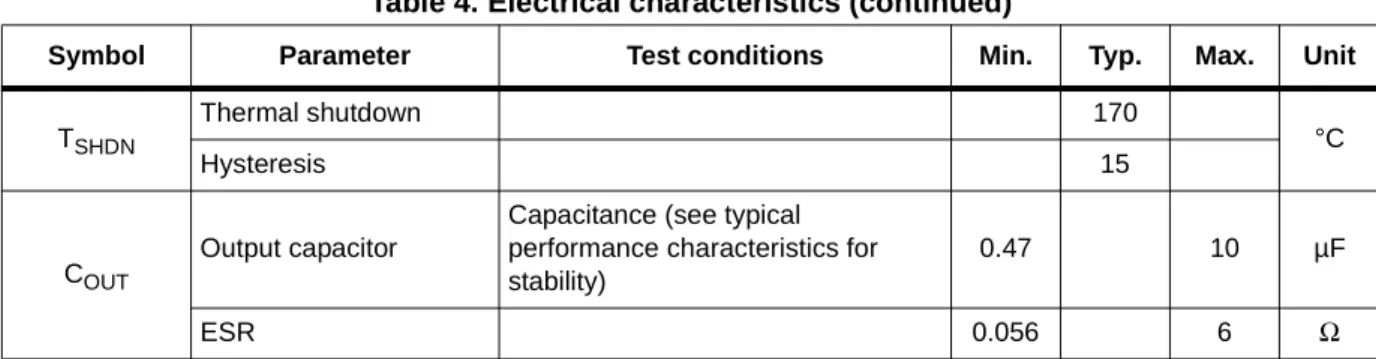
TSHDN Thermal shutdown 170 °C
Hysteresis 15
COUT
Output capacitor
Capacitance (see typical performance characteristics for stability)
0.47 10 µF
ESR 0.056 6 Ω
1. Dropout voltage is the input-to-output voltage difference at which the output voltage is 100 mV below its nominal value. This specification does not apply to output voltages below 1.5 V.
2. During shutdown and at no load, P-channel leakage current flowing through the internal resistor divider causes the VOUT rise.
3. Turn-on time is the time measured between the enable input just exceeding VEN high value and the output voltage just
reaching 95% of its nominal value.
Table 4. Electrical characteristics (continued)
Typical performance characteristics STLQ015
6
Typical performance characteristics
Figure 4. Output voltage vs. temperature Figure 5. Output voltage vs. input voltage
(VOUT= 0.8 V)
Figure 6. Output voltage vs. input voltage
(VOUT= 3.3 V)
Figure 7. Dropout voltage vs. temperature
-1.00% -0.80% -0.60% -0.40% -0.20% 0.00% 0.20% 0.40% 0.60% 0.80% 1.00%
-40 -20 0 20 40 60 80 100 120 140
Temperature [°C] VOU T va ria ti o n [% ]
IOUT= 1 mA
-1.00% -0.80% -0.60% -0.40% -0.20% 0.00% 0.20% 0.40% 0.60% 0.80% 1.00%
-40 -20 0 20 40 60 80 100 120 140
Temperature [°C] VOU T va ria ti o n [% ]
IOUT= 1 mA
0.0 0.2 0.4 0.6 0.8 1.0
0.3 0.5 0.7 0.9 1.1 1.3 1.5 1.7 1.9
VIN[V] VOUT [V ] T= -40°C T= +25°C T= 125°C
IOUT= 150 mA, VOUT= 0.8 V
0.0 0.2 0.4 0.6 0.8 1.0
0.3 0.5 0.7 0.9 1.1 1.3 1.5 1.7 1.9
VIN[V] VOUT [V ] T= -40°C T= +25°C T= 125°C
IOUT= 150 mA, VOUT= 0.8 V
0.0 0.4 0.8 1.2 1.6 2.0 2.4 2.8 3.2 3.6
0.0 0.5 1.0 1.5 2.0 2.5 3.0 3.5 4.0 4.5 5.0 5.5
VIN[V] VOUT [V ] T= -40°C T= +25°C T= 125°C
IOUT= 150 mA, VOUT= 3.3 V
0.0 0.4 0.8 1.2 1.6 2.0 2.4 2.8 3.2 3.6
0.0 0.5 1.0 1.5 2.0 2.5 3.0 3.5 4.0 4.5 5.0 5.5
VIN[V] VOUT [V ] T= -40°C T= +25°C T= 125°C
IOUT= 150 mA, VOUT= 3.3 V
0.05 0.10 0.15 0.20 0.25 0.30
-40 -20 0 20 40 60 80 100 120 140
Temperature [°C]
Vd
ro
p
[V]
VO = 1.5 V
VO = 3.3 V
IOUT= 150 mA
0.05 0.10 0.15 0.20 0.25 0.30
-40 -20 0 20 40 60 80 100 120 140
Temperature [°C]
Vd
ro
p
[V]
VO = 1.5 V
VO = 3.3 V
DocID17285 Rev 5 11/18
STLQ015 Typical performance characteristics
18
Figure 8. Dropout voltage vs. output current Figure 9. Quiescent current vs. temperature
0.00 0.05 0.10 0.15 0.20 0.25 0.30
0 0.05 0.1 0.15 0.2
IOUT[A]
Vd
ro
p
[V]
VO = 1.5 V
VO = 3.3 V
0.00 0.05 0.10 0.15 0.20 0.25 0.30
0 0.05 0.1 0.15 0.2
IOUT[A]
Vd
ro
p
[V]
VO = 1.5 V
VO = 3.3 V
0.00 0.20 0.40 0.60 0.80 1.00 1.20 1.40 1.60 1.80 2.00
-40 -20 0 20 40 60 80 100 120 140
Temperature [°C]
Iq
[µ
A
]
VIN = 1.5 V, VO = 0.8 V
VIN = 4.3 V, VO = 3.3 V
IO = 0 mA
0.00 0.20 0.40 0.60 0.80 1.00 1.20 1.40 1.60 1.80 2.00
-40 -20 0 20 40 60 80 100 120 140
Temperature [°C]
Iq
[µ
A
]
VIN = 1.5 V, VO = 0.8 V
VIN = 4.3 V, VO = 3.3 V
IO = 0 mA
Figure 10. Supply voltage rejection vs. frequency
Figure 11. Supply voltage rejection vs. IOUT
Figure 12. Quiescent current vs. input voltage Figure 13. Quiescent current vs. output current
10 20 30 40 50 60 70
100 1000 10000 100000
f [Hz] S uppl y V o lt age r e je c ti on [ d B ] Vout=0.8V Vout=3.3V 0 10 20 30 40 50
0 20 40 60 80 100 120 140 160
IOUT[mA]
Su pply Volt ag e Re je ction [d b]
VIN = 1.5, VO = 0.8 V
VIN = 4.3 V, VO = 3.3 V
f = 1 kHz
0 10 20 30 40 50
0 20 40 60 80 100 120 140 160
IOUT[mA]
Su pply Volt ag e Re je ction [d b]
VIN = 1.5, VO = 0.8 V
VIN = 4.3 V, VO = 3.3 V
f = 1 kHz
0.00 0.20 0.40 0.60 0.80 1.00 1.20 1.40 1.60 1.80 2.00 2.20 2.40
0.0 0.5 1.0 1.5 2.0 2.5 3.0 3.5 4.0 4.5 5.0 5.5
VIN[V]
Iq
[µ
A
]
VO = 0.8 V
VO = 3.3 V
IO = 1 mA
0.00 0.20 0.40 0.60 0.80 1.00 1.20 1.40 1.60 1.80 2.00 2.20 2.40
0.0 0.5 1.0 1.5 2.0 2.5 3.0 3.5 4.0 4.5 5.0 5.5
VIN[V]
Iq
[µ
A
]
VO = 0.8 V
VO = 3.3 V
IO = 1 mA
0.00 0.20 0.40 0.60 0.80 1.00 1.20 1.40 1.60 1.80 2.00
0 20 40 60 80 100 120 140 160
IOUT[mA]
Iq
[µ
A
]
VIN= 4.3 V, VO= 3.3 V
VIN= 1.5 V, VO= 0.8 V
TJ= 25 °C
0.00 0.20 0.40 0.60 0.80 1.00 1.20 1.40 1.60 1.80 2.00
0 20 40 60 80 100 120 140 160
IOUT[mA]
Iq
[µ
A
]
VIN= 4.3 V, VO= 3.3 V
VIN= 1.5 V, VO= 0.8 V
Typical performance characteristics STLQ015
Figure 14. Output noise voltage vs. frequency Figure 15. COUT stability region
0.0 2.0 4.0 6.0 8.0 10.0 12.0 14.0 16.0 18.0
10 100 f [Hz] 1000 10000 100000
e N [ u V/ SQ R T (H z )]
3V3 Iload= 10mA 0V8 Iload= 10mA
0.00 1.00 2.00 3.00 4.00 5.00 6.00 7.00 8.00
0.0 1.0 2.0 3.0 4.0 5.0 6.0 7.0 8.0 9.0 10.0 COUT[µF]
ESR at 100 kH z [ ohm ] ESR MAX ESR MIN 0.00 1.00 2.00 3.00 4.00 5.00 6.00 7.00 8.00
0.0 1.0 2.0 3.0 4.0 5.0 6.0 7.0 8.0 9.0 10.0 COUT[µF]
ESR at 100 kH z [ ohm ] ESR MAX ESR MIN
Figure 16. Start-up transient Figure 17. Enable transient
VIN from 0 to 1.5 V, VEN tied to VIN, no load COUT = 1 µF
VIN = 1.5 V; VEN from 0 to 2 V, no load, T = 25 °C
VOUT VIN VOUT VIN VOUT VEN VOUT VEN
DocID17285 Rev 5 13/18
STLQ015 Package information
18
7 Package
information
In order to meet environmental requirements, ST offers these devices in different grades of ECOPACK® packages, depending on their level of environmental compliance. ECOPACK® specifications, grade definitions and product status are available at: www.st.com.
ECOPACK® is an ST trademark.
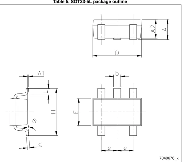
Table 5. SOT23-5L package outline
Package information STLQ015
Table 6. SOT23-5L package mechanical data
Figure 18. SOT23-5L recommended footprint (dimensions in mm)
Dim.
mm
Min. Typ. Max.
A 0.90 1.45
A1 0 0.15
A2 0.90 1.30
b 0.30 0.50
c 2.09 0.20
D 2.95
E 1.60
e 0.95
H 2.80
L 0.30 0.60
θ 0 8
DocID17285 Rev 5 15/18
STLQ015 Package information
18
7.1
Packaging mechanical data
Figure 19.Tape and reel SOT23-5L drawings
Table 7. Tape and reel SOT23-5L mechanical data
Dim.
mm
Min. Typ. Max.
A 180
C 12.8 13.0 13.2
D 20.2
N 60
T 14.4
Ao 3.13 3.23 3.33
Bo 3.07 3.17 3.27
Ko 1.27 1.37 1.47
Po 3.9 4.0 4.1
Order code STLQ015
8 Order
code
Table 8. Device summary
Order codes Output voltages Package Marking
STLQ015M12R 1.2 V
SOT23-5L
1512
STLQ015M15R 1.5 V 1515
STLQ015M18R 1.8 V 1518
STLQ015M21R 2.1 V 1521
STLQ015M25R 2.5 V 1525
STLQ015M28R 2.8 V 1528
STLQ015M30R 3.0 V 1530
DocID17285 Rev 5 17/18
STLQ015 Revision history
18
9 Revision
history
Table 9. Document revision history
Date Revision Changes
23-Mar-2010 1 Initial release.
20-Jan-2011 2 Modified: Table 5 on page 13 and Figure 18. Added: Figure 19.
11-Sep-2012 3 Added: new order codes STLQ015XG12R, STLQ015XG15R and STLQ015XG18R to the device summary table.
17-Feb-2014 4
Changed the part number STLQ015xx to STLQ015. Changed the title in cover page.
Updated Description and Table : in cover page.
Changed typ. value of IQ parameter in Table 4: Electrical characteristics. Minor text changes.
03-Jul-2015 5
Added package SOT23-5L.
Updated Table 1.: Pin description, Table 3.: Thermal data and Figure 2.: Pin configuration (top view)
Updated 8: Order code.
Updated Section 7: Package information. Minor text changes.
STLQ015
IMPORTANT NOTICE – PLEASE READ CAREFULLY
STMicroelectronics NV and its subsidiaries (“ST”) reserve the right to make changes, corrections, enhancements, modifications, and improvements to ST products and/or to this document at any time without notice. Purchasers should obtain the latest relevant information on ST products before placing orders. ST products are sold pursuant to ST’s terms and conditions of sale in place at the time of order acknowledgement.
Purchasers are solely responsible for the choice, selection, and use of ST products and ST assumes no liability for application assistance or the design of Purchasers’ products.
No license, express or implied, to any intellectual property right is granted by ST herein.
Resale of ST products with provisions different from the information set forth herein shall void any warranty granted by ST for such product.
ST and the ST logo are trademarks of ST. All other product or service names are the property of their respective owners.
Information in this document supersedes and replaces information previously supplied in any prior versions of this document.