Single-Supply TTL/CMOS Comparators
ADCMP600/ADCMP601/ADCMP602
FEATURES
Fully specified rail to rail at VCC = 2.5 V to 5.5 V
Input common-mode voltage from −0.2 V to VCC + 0.2 V Low glitch CMOS-/TTL-compatible output stage 3.5 ns propagation delay
10 mW at 3.3 V Shutdown pin
Single-pin control for programmable hysteresis and latch Power supply rejection > 50 dB
Improved replacement for MAX999 −40°C to +125°C operation
APPLICATIONS
High speed instrumentation Clock and data signal restoration Logic level shifting or translation Pulse spectroscopy
High speed line receivers Threshold detection
Peak and zero-crossing detectors High speed trigger circuitry Pulse-width modulators
Current/voltage-controlled oscillators Automatic test equipment (ATE)
FUNCTIONAL BLOCK DIAGRAM
NONINVERTING INPUT INVERTING INPUT LE/HYS (EXCEPT ADCMP600) Q OUTPUT SDN (ADCMP602 ONLY) ADCMP600/ ADCMP601/ ADCMP602 05914-001 Figure 1.
GENERAL DESCRIPTION
The ADCMP600, ADCMP601, and ADCMP602 are very fast comparators fabricated on XFCB2, an Analog Devices, Inc. proprietary process. These comparators are exceptionally versatile and easy to use. Features include an input range from GND − 0.5 V to VCC + 0.2 V, low noise, TTL-/CMOS-compatible output drivers, and latch inputs with adjustable hysteresis and/or shutdown inputs.
The device offers 5 ns propagation delay with 10 mV overdrive on 3 mA typical supply current.
A flexible power supply scheme allows the devices to operate with a single +2.5 V positive supply and a −0.5 V to +2.8 V input signal range up to a +5.5 V positive supply with a −0.5 V to +5.8 V input signal range. Split input/output supplies with no sequencing restrictions on the ADCMP602 support a wide
input signal range while still allowing independent output swing control and power savings.
The TTL-/CMOS-compatible output stage is designed to drive up to 5 pF with full timing specs and to degrade in a graceful and linear fashion as additional capacitance is added. The comparator input stage offers robust protection against large input overdrive, and the outputs do not phase reverse when the valid input signal range is exceeded. Latch and programmable hysteresis features are also provided with a unique single-pin control option.
The ADCMP600 is available in 5-lead SC70 and SOT-23 packages, the ADCMP601 is available in a 6-lead SC70 package, and the ADCMP602 is available in an 8-lead MSOP package.
TABLE OF CONTENTS
Features ... 1
Applications ... 1
Functional Block Diagram ... 1
General Description ... 1
Revision History ... 2
Specifications ... 3
Electrical Characteristics ... 3
Timing Information ... 5
Absolute Maximum Ratings ... 6
Thermal Resistance ... 6
ESD Caution ... 6
Pin Configuration and Function Descriptions ... 7
Typical Performance Characteristics ... 8
Application Information ... 10
Power/Ground Layout and Bypassing ... 10
TTL-/CMOS-Compatible Output Stage ... 10
Using/Disabling the Latch Feature ... 10
Optimizing Performance ... 11
Comparator Propagation Delay Dispersion ... 11
Comparator Hysteresis ... 11
Crossover Bias Point ... 12
Minimum Input Slew Rate Requirement ... 12
Typical Application Circuits ... 13
Outline Dimensions ... 14
Ordering Guide ... 16
REVISION HISTORY
1/11—Rev. 0 to Rev. A Changed VEE Pin to GND ... Throughout Changes to Common-Mode Dispersion Conditions... 4Changes to Figure 15 and Figure 16 ... 9
Changes to Comparator Hysteresis Section ... 12
Updated Outline Dimensions ... 14
Changes to Ordering Guide ... 15
SPECIFICATIONS
ELECTRICAL CHARACTERISTICS
VCCI = VCCO = 2.5 V, TA = 25°C, unless otherwise noted.
Table 1.
Parameter Symbol Conditions Min Typ Max Unit
DC INPUT CHARACTERISTICS
Voltage Range VP, VN VCC = 2.5 V to 5.5 V −0.5 VCC + 0.2 V
Common-Mode Range VCC = 2.5 V to 5.5 V −0.2 VCC + 0.2 V
Differential Voltage VCC = 2.5 V to 5.5 V VCC + 0.8 V
Offset Voltage VOS −5.0 ±2 +5.0 mV
Bias Current IP, IN −5.0 ±2 +5.0 µA
Offset Current −2.0 +2.0 µA
Capacitance CP, CN 1 pF
Resistance, Differential Mode −0.1 V to VCC 200 700 kΩ
Resistance, Common Mode −0.5 V to VCC + 0.5 V 100 350 kΩ
Active Gain AV 85 dB
Common-Mode Rejection Ratio CMRR VCCI = 2.5 V, VCCO = 2.5 V,
VCM = −0.2 V to +2.7 V
50 dB
VCCI = 2.5 V, VCCO = 5.5 V 50 dB
Hysteresis (ADCMP600) 2 mV
Hysteresis (ADCMP601/ADCMP602) RHYS = ∞ 0.1 mV
LATCH ENABLE PIN CHARACTERISTICS (ADCMP601/ADCMP602 Only)
VIH Hysteresis is shut off 2.0 VCC V
VIL Latch mode guaranteed −0.2 +0.4 +0.8 V
IIH VIH = VCC −6 +6 µA
IOL VIL = 0.4 V −0.1 +0.1 mA
HYSTERESIS MODE AND TIMING (ADCMP601/ADCMP602 Only)
Hysteresis Mode Bias Voltage Current −1 μA 1.145 1.25 1.35 V Resistor Value Hysteresis = 120 mV 65 80 120 kΩ Hysteresis Current Hysteresis = 120 mV −18 −12 −7 µA
Latch Setup Time tS VOD = 50 mV −2 ns
Latch Hold Time tH VOD = 50 mV 2.6 ns
Latch-to-Output Delay tPLOH, tPLOL VOD = 50 mV 27 ns
Latch Minimum Pulse Width tPL VOD = 50 mV 21 ns
SHUTDOWN PIN CHARACTERISTICS (ADCMP602 Only)
VIH Comparator is operating 2.0 VCCO V
VIL Shutdown guaranteed −0.2 +0.4 +0.6 V
IIH VIH = VCC −6 6 µA
IOL VIL = 0 V −100 µA
Sleep Time tSD ICCO < 500 µA 20 ns
Wake-Up Time tH VOD = 100 mV, output valid 50 ns
DC OUTPUT CHARACTERISTICS VCCO = 2.5 V to 5.5 V
Output Voltage High Level VOH IOH = 8 mA, VCCO = 2.5 V VCC − 0.4 V
Output Voltage Low Level VOL IOL = 8 mA, VCCO = 2.5 V 0.4 V
Parameter Symbol Conditions Min Typ Max Unit
AC PERFORMANCE1
Rise Time /Fall Time tR tF 10% to 90%, VCCO = 2.5 V 2.2 ns
10% to 90%, VCCO = 5.5 V 4 ns
Propagation Delay tPD VOD = 50 mV, VCCO = 2.5 V 3.5 ns
VOD = 50 mV, VCCO = 5.5 V 4.3 ns
VOD = 10 mV, VCCO = 2.5 V 5 ns
Propagation Delay Skew—Rising to Falling Transition
VCCO = 2.5 V to 5.5 V
VOD = 50 mV
500 ps
Overdrive Dispersion 10 mV < VOD < 125 mV 1.2 ns
Common-Mode Dispersion −0.2 V < VCM < VCCI + 0.2 V
VOD = 50 mV
200 ps
Minimum Pulse Width PWMIN VCCI = VCCO = 2.5 V
PWOUT = 90% of PWIN 3 ns VCCI = VCCO = 5.5 V PWOUT = 90% of PWIN 4.5 ns POWER SUPPLY
Input Supply Voltage Range VCCI 2.5 5.5 V
Output Supply Voltage Range VCCO 2.5 5.5 V
Positive Supply Differential VCCI − VCCO Operating −3.0 +3.0 V
(ADCMP602 Only)
VCCI − VCCO Nonoperating −5.5 +5.5 V
Positive Supply Current (ADCMP600/ADCMP601) IVCC VCC = 2.5 V VCC = 5.5 V 3 3.5 3.5 4.0 mA Input Section Supply Current IVCCI VCCI = 2.5 V 0.9 1.4 mA
(ADCMP602 Only) VCCI = 5.5 V 1.2 2.0 mA
Output Section Supply Current IVCCO VCCO = 2.5 V 1.45 3.0 mA
(ADCMP602 Only) VCCO = 5.5 V 2.1 3.5 mA
Power Dissipation PD VCC = 2.5 V 7 9 mW
PD VCC = 5.5 V 20 23 mW
Power Supply Rejection Ratio PSRR VCCI = 2.5 V to 5 V −50 dB
Shutdown Mode ICCI VCC = 2.5 V 240 400 µA
(ADCMP602 Only)
Shutdown Mode ICCO VCC =2.5 V 30 µA
(ADCMP602 Only)
1 V
TIMING INFORMATION
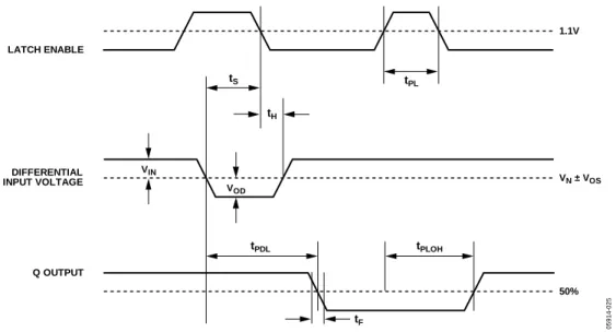
Figure 2 illustrates the ADCMP600/ADCMP601/ADCMP602 latch timing relationships. Table 2 provides definitions of the terms shown in Figure 2. 1.1V 50% VN ± VOS DIFFERENTIAL INPUT VOLTAGE LATCH ENABLE Q OUTPUT tH tPDL tPLOH tF VIN VOD tS tPL 05914-025
Figure 2. System Timing Diagram
Table 2. Timing Descriptions
Symbol Timing Description
tPDH Input to output high delay Propagation delay measured from the time the input signal crosses the reference (± the
input offset voltage) to the 50% point of an output low-to-high transition.
tPDL Input to output low delay Propagation delay measured from the time the input signal crosses the reference (± the
input offset voltage) to the 50% point of an output high-to-low transition.
tPLOH Latch enable to output high delay Propagation delay measured from the 50% point of the latch enable signal low-to-high
transition to the 50% point of an output low-to-high transition.
tPLOL Latch enable to output low delay Propagation delay measured from the 50% point of the latch enable signal low-to-high
transition to the 50% point of an output high-to-low transition.
tH Minimum hold time Minimum time after the negative transition of the latch enable signal that the input signal
must remain unchanged to be acquired and held at the outputs.
tPL Minimum latch enable pulse width Minimum time that the latch enable signal must be high to acquire an input signal change.
tS Minimum setup time Minimum time before the negative transition of the latch enable signal occurs that an
input signal change must be present to be acquired and held at the outputs.
tR Output rise time Amount of time required to transition from a low to a high output as measured at the 20%
and 80% points.
tF Output fall time Amount of time required to transition from a high to a low output as measured at the 20%
and 80% points.
ABSOLUTE MAXIMUM RATINGS
Table 3.
Parameter Rating
Supply Voltages
Input Supply Voltage (VCCI to GND) −0.5 V to +6.0 V
Output Supply Voltage (VCCO to GND)
−0.5 V to +6.0 V Positive Supply Differential
(VCCI − VCCO)
−6.0 V to +6.0 V Input Voltages
Input Voltage −0.5 V to VCCI + 0.5 V
Differential Input Voltage ±(VCCI + 0.5 V)
Maximum Input/Output Current ±50 mA Shutdown Control Pin
Applied Voltage (HYS to GND) −0.5 V to VCCO + 0.5 V
Maximum Input/Output Current ±50 mA Latch/Hysteresis Control Pin
Applied Voltage (HYS to GND) −0.5 V to VCCO + 0.5 V
Maximum Input/Output Current ±50 mA Output Current ±50 mA Temperature
Operating Temperature, Ambient −40°C to +125°C Operating Temperature, Junction 150°C
Storage Temperature Range −65°C to +150°C
Stresses above those listed under Absolute Maximum Ratings may cause permanent damage to the device. This is a stress rating only; functional operation of the device at these or any other conditions above those indicated in the operational section of this specification is not implied. Exposure to absolute maximum rating conditions for extended periods may affect device reliability.
THERMAL RESISTANCE
θJA is specified for the worst-case conditions, that is, a device soldered in a circuit board for surface-mount packages.
Table 4. Thermal Resistance
Package Type θJA1 Unit
ADCMP600 SC70 5-Lead 426 °C/W ADCMP600 SOT-23 5-Lead 302 °C/W ADCMP601 SC70 6-Lead 426 °C/W ADCMP602 MSOP 5-Lead 130 °C/W
1 Measurement in still air.
ESD CAUTION
PIN CONFIGURATION AND FUNCTION DESCRIPTIONS
Q 1 VP 3 GND 2 VCCI/VCCO 5 VN 4 ADCMP600 TOP VIEW (Not to Scale) 05914-002 Q 1 GND 2 VP 3 VCCI/VCCO 6 LE/HYS 5 VN 4 ADCMP601 TOP VIEW (Not to Scale) 05914-003 VCCI 1 VP 2 VN 3 SDN 4 VCCO 8 Q 7 GND 6 LE/HYS 5 ADCMP602 TOP VIEW (Not to Scale) 05914-004Figure 3. ADCMP600 Pin Configuration Figure 4. ADCMP601 Pin Configuration Figure 5. ADCMP602 Pin Configuration
Table 5. ADCMP600 (SOT-23-5 and SC70-5) Pin Function Descriptions
Pin No. Mnemonic Description
1 Q Noninverting Output. Q is at logic high if the analog voltage at the noninverting input, VP, is greater
than the analog voltage at the inverting input, VN.
2 GND Negative Supply Voltage. 3 VP Noninverting Analog Input.
4 VN Inverting Analog Input.
5 VCCI/VCCO Input Section Supply/Output Section Supply. Shared pin.
Table 6. ADCMP601 (SC70-6) Pin Function Descriptions
Pin No. Mnemonic Description
1 Q Noninverting Output. Q is at logic high if the analog voltage at the noninverting input, VP, is greater
than the analog voltage at the inverting input, VN, if the comparator is in compare mode.
2 GND Negative Supply Voltage. 3 VP Noninverting Analog Input.
4 VN Inverting Analog Input.
5 LE/HYS Latch/Hysteresis Control. Bias with resistor or current for hysteresis adjustment; drive low to latch. 6 VCCI/VCCO Input Section Supply/Output Section Supply. Shared pin.
Table 7. ADCMP602 (MSOP-8) Pin Function Descriptions
Pin No. Mnemonic Description
1 VCCI Input Section Supply.
2 VP Noninverting Analog Input.
3 VN Inverting Analog Input.
4 SDN Shutdown. Drive this pin low to shut down the device.
5 LE/HYS Latch/Hysteresis Control. Bias with resistor or current for hysteresis adjustment; drive low to latch. 6 GND Negative Supply Voltage.
7 Q Noninverting Output. Q is at logic high if the analog voltage at the noninverting input, VP, is greater
than the analog voltage at the inverting input, VN, if the comparator is in compare mode.
TYPICAL PERFORMANCE CHARACTERISTICS
VCCI = VCCO = 2.5 V, TA = 25°C, unless otherwise noted.
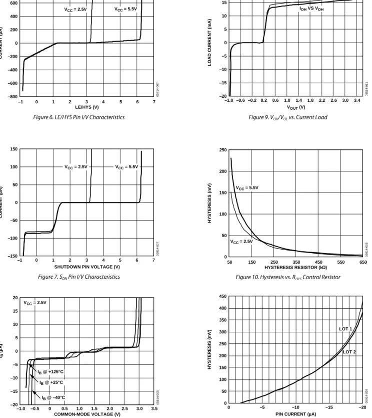
–800 –1 0 1 2 3 4 5 6 7 –600 –400 –200 0 200 400 600 800 05914-007 CURRE NT ( µ A) LE/HYS (V) VCC= 5.5V VCC= 2.5V
Figure 6. LE/HYS Pin I/V Characteristics
150 –150 –100 –50 0 50 100 –1 0 1 2 3 4 5 6 7 05914-027 CURRE NT ( µ A)
SHUTDOWN PIN VOLTAGE (V) VCC = 2.5V VCC = 5.5V
Figure 7. SDN Pin I/V Characteristics
05914-005 IB ( µ A) COMMON-MODE VOLTAGE (V) –20 –15 15 –10 10 –5 5 0 20 –1.0 –0.5 0 0.5 1.0 1.5 2.0 2.5 3.0 3.5 IB @ +125°C IB @ +25°C VCC = 2.5V IB @ –40°C
Figure 8. Input Bias Current vs. Input Common Mode
20 –5 5 0 –10 10 –15 15 –20 –1.0 –0.6 –0.2 0.2 0.6 1.0 1.4 1.8 2.2 2.6 3.0 3.4 09514-011 L O AD CURRE NT ( mA) VOUT (V) IOH VS VOH IOL VS VOL
Figure 9. VOH/VOL vs. Current Load
0 50 150 250 350 450 550 650 50 100 150 200 250 05914-008 H YST ER ESI S (m V) HYSTERESIS RESISTOR (kΩ) VCC= 5.5V VCC= 2.5V
Figure 10. Hysteresis vs. RHYS Control Resistor
450 0 50 100 150 200 250 300 350 400 0 –5 –10 –15 –20 05914-026 H YST ER ESI S (m V)
PIN CURRENT (µA)
LOT 1
LOT 2
4.8 3.0 3.2 3.4 3.6 3.8 4.0 4.2 4.4 4.6 0 10 20 30 40 50 60 70 80 90 100 110 120 130 140 05914-009 P RO P AG AT IO N DE L AY ( n s) OVERDRIVE (mV)
Figure 12. Propagation Delay vs. Input Overdrive at VCC = 2.5 V
4.0 3.8 3.4 3.6 3.2 3.0 –0.6 0 0.6 1.2 1.8 2.4 3.0 05914-028 P RO P AG AT IO N DE L AY ( n s) COMMON-MODE VOLTAGE (V) VCM AT VCC = 2.5V RISE FALL
Figure 13. Propagation Delay vs. Input Common-Mode Voltage at VCC = 2.5 V 5.0 3.0 3.2 3.4 3.6 3.8 4.0 4.2 4.4 4.6 4.8 2.5 3.0 3.5 4.0 4.5 5.0 5.5 6.0 05914-029 P RO P AG AT IO N DE L AY ( n s) VCCO (V) RISE FALL
Figure 14. Propagation Delay vs. VCCO
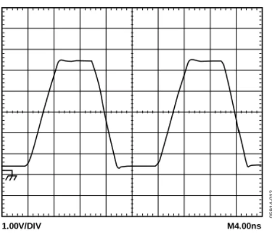
05914-012
1.00V/DIV M4.00ns
Figure 15. 50 MHz Output Waveform VCC = 5.5 V
05914-013
500mV/DIV M4.00ns
APPLICATION INFORMATION
POWER/GROUND LAYOUT AND BYPASSING
The ADCMP600/ADCMP601/ADCMP602 comparators are very high speed devices. Despite the low noise output stage, it is essential to use proper high speed design techniques to achieve the specified performance. Because comparators are uncompensated amplifiers, feedback in any phase relationship is likely to cause oscillations or undesired hysteresis. Of critical importance is the use of low impedance supply planes, particularly the output supply plane (VCCO) and the ground plane (GND). Individual supply planes are recommended as part of a multilayer board. Providing the lowest inductance return path for switching currents ensures the best possible performance in the target application.
It is also important to adequately bypass the input and output supplies. Multiple high quality 0.01 µF bypass capacitors should be placed as close as possible to each of the VCCI and VCCO supply pins and should be connected to the GND plane with redundant vias. At least one of these should be placed to provide a physically short return path for output currents flowing back from ground to the VCC pin. High frequency bypass capacitors should be carefully selected for minimum inductance and ESR. Parasitic layout inductance should also be strictly controlled to maximize the effectiveness of the bypass at high frequencies.
If the package allows and the input and output supplies have been connected separately such that VCCI ≠ VCCO, care should be taken to bypass each of these supplies separately to the GND plane. A bypass capacitor should never be connected between them. It is recommended that the GND plane separate the VCCI and VCCO planes when the circuit board layout is designed to minimize coupling between the two supplies and to take advantage of the additional bypass capacitance from each respective supply to the ground plane. This enhances the performance when split input/output supplies are used. If the input and output supplies are connected together for single-supply operation such that VCCI = VCCO, coupling between the two supplies is unavoidable; however, careful board placement can help keep output return currents away from the inputs.
TTL-/CMOS-COMPATIBLE OUTPUT STAGE
Specified propagation delay performance can be achieved only by keeping the capacitive load at or below the specified minimums. The outputs of the devices are designed to directly drive one Schottky TTL or three low power Schottky TTL loads or the equivalent. For large fan outputs, buses, or transmission lines, use an appropriate buffer to maintain the excellent speed and stability of the comparator.
With the rated 5 pF load capacitance applied, more than half of the total device propagation delay is output stage slew time, even at 2.5 V VCC. Because of this, the total prop delay decreases as VCCO decreases, and instability in the power supply may appear as excess delay dispersion.
This delay is measured to the 50% point for the supply in use; therefore, the fastest times are observed with the VCC supply at 2.5 V, and larger values are observed when driving loads that switch at other levels.
When duty cycle accuracy is critical, the logic being driven should switch at 50% of VCC and load capacitance should be minimized. When in doubt, it is best to power VCCO or the entire device from the logic supply and rely on the input PSRR and CMRR to reject noise.
Overdrive and input slew rate dispersions are not significantly affected by output loading and VCC variations.
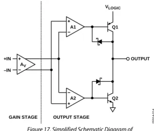
The TTL-/CMOS-compatible output stage is shown in the simplified schematic diagram (Figure 17). Because of its inherent symmetry and generally good behavior, this output stage is readily adaptable for driving various filters and other unusual loads. OUTPUT Q2 Q1 +IN –IN OUTPUT STAGE VLOGIC GAIN STAGE A2 A1 AV 05914-014
Figure 17. Simplified Schematic Diagram of TTL-/CMOS-Compatible Output Stage
USING/DISABLING THE LATCH FEATURE
The latch input is designed for maximum versatility. It can safely be left floating for fixed hysteresis or be tied to VCC to remove the hysteresis, or it can be driven low by any standard TTL/CMOS device as a high speed latch.
In addition, the pin can be operated as a hysteresis control pin with a bias voltage of 1.25 V nominal and an input resistance of approximately 7000 Ω. This allows the comparator hysteresis to be easily and accurately controlled by either a resistor or an inexpensive CMOS DAC.
Hysteresis control and latch mode can be used together if an open drain, an open collector, or a three-state driver is connected parallel to the hysteresis control resistor or current source. Due to the programmable hysteresis feature, the logic threshold of the latch pin is approximately 1.1 V regardless of VCC.
OPTIMIZING PERFORMANCE
As with any high speed comparator, proper design and layout techniques are essential for obtaining the specified performance. Stray capacitance, inductance, inductive power and ground impedances, or other layout issues can severely limit performance and often cause oscillation. Large discontinuities along input and output transmission lines can also limit the specified pulse-width dispersion performance. The source impedance should be minimized as much as is practicable. High source impedance, in combination with the parasitic input capacitance of the comparator, causes an undesirable degradation in bandwidth at the input, thus degrading the overall response. Thermal noise from large resistances can easily cause extra jitter with slowly slewing input signals; higher impedances encourage undesired coupling.
COMPARATOR PROPAGATION DELAY
DISPERSION
The ADCMP600/ADCMP601/ADCMP602 comparators are designed to reduce propagation delay dispersion over a wide input overdrive range. Propagation delay dispersion is the variation in propagation delay that results from a change in the degree of overdrive or slew rate (that is, how far or how fast the input signal exceeds the switching threshold).
Propagation delay dispersion is a specification that becomes important in high speed, time-critical applications, such as data communication, automatic test and measurement, and instru-mentation. It is also important in event-driven applications, such as pulse spectroscopy, nuclear instrumentation, and medical imaging. Dispersion is defined as the variation in propagation delay as the input overdrive conditions are changed (Figure 18 and Figure 19).
The device dispersion is typically < 2 ns as the overdrive varies from 10 mV to 125 mV. This specification applies to both positive and negative signals because the device has very closely matched delays both positive-going and negative-going inputs.
Q/Q OUTPUT INPUT VOLTAGE 500mV OVERDRIVE 10mV OVERDRIVE DISPERSION VN ± VOS 05 91 4-0 15
Figure 18. Propagation Delay—Overdrive Dispersion
Q/Q OUTPUT 10V/ns 1V/ns DISPERSION VN ± VOS 05 91 4-0 1 6
Figure 19. Propagation Delay—Slew Rate Dispersion
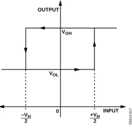
COMPARATOR HYSTERESIS
The addition of hysteresis to a comparator is often desirable in a noisy environment, or when the differential input amplitudes are relatively small or slow moving. Figure 20 shows the transfer function for a comparator with hysteresis. As the input voltage approaches the threshold (0.0 V, in this example) from below the threshold region in a positive direction, the comparator switches from low to high when the input crosses +VH/2, and the new switching threshold becomes −VH/2. The comparator remains in the high state until the new threshold, −VH/2, is crossed from below the threshold region in a negative direction. In this manner, noise or feedback output signals centered on 0.0 V input cannot cause the comparator to switch states unless it exceeds the region bounded by ±VH/2. OUTPUT INPUT 0 VOL VOH +VH 2 –VH 2 059 14 -01 7
Figure 20. Comparator Hysteresis Transfer Function
The customary technique for introducing hysteresis into a comparator uses positive feedback from the output back to the input. One limitation of this approach is that the amount of hysteresis varies with the output logic levels, resulting in hysteresis that is not symmetric about the threshold. The external feedback network can also introduce significant parasitics that reduce high speed performance and induce oscillation in some cases.
These ADCMP600 features a fixed hysteresis of approximately 2 mV. The ADCMP601 and ADCMP602 comparators offer a
Leaving the LE/HYS pin disconnected results in a fixed
hysteresis of 2 mV; driving this pin high removes hysteresis. The maximum hysteresis that can be applied using this pin is approximately 160 mV. Figure 21 illustrates the amount of hysteresis applied as a function of the external resistor value, and Figure 11 illustrates hysteresis as a function of the current. The hysteresis control pin appears as a 1.25 V bias voltage seen through a series resistance of 7 kΩ. The bias voltage changes ± 20% throughout the hysteresis control range. The advantages of applying hysteresis in this manner are improved accuracy, improved stability, reduced component count, and maximum versatility. An external bypass capacitor is not recommended on the HYS pin because it impairs the latch function and often degrades the jitter performance of the device. As described in the Using/Disabling the Latch Feature section, hysteresis control need not compromise the latch function.
CROSSOVER BIAS POINT
In both op amps and comparators, rail-to-rail inputs of this type have a dual front-end design. Certain devices are active near the VCC rail and others are active near the GND rail. At some predeter-mined point in the common-mode range, a crossover occurs. At this point, normally VCC/2, the direction of the bias current reverses and the measured offset voltages and currents change.
The ADCMP600/ADCMP601/ADCMP602 comparators slightly elaborate on this scheme. Crossover points can be found at approximately 0.8 V and 1.6 V. 0 50 150 250 350 450 550 650 50 100 150 200 250 05914-030 H YST ER ESI S (m V) HYSTERESIS RESISTOR (kΩ) VCC= 5.5V VCC= 2.5V
Figure 21. Hysteresis vs. RHYS Control Resistor
MINIMUM INPUT SLEW RATE REQUIREMENT
With the rated load capacitance and normal good PC Board design practice, as discussed in the Optimizing Performance section, these comparators should be stable at any input slew rate with no hysteresis. Broadband noise from the input stage is observed in place of the violent chattering seen with most other high speed comparators. With additional capacitive loading or poor bypassing, oscillation is observed. This oscillation is due to the high gain bandwidth of the comparator in combination with feedback parasitics in the package and PC board. In many applications, chattering is not harmful.
TYPICAL APPLICATION CIRCUITS
OUTPUT ADCMP600 0.1µF 5V 0.1µF 2kΩ 2kΩ 05914-019Figure 22. Self-Biased, 50% Slicer
CMOS ADCMP600 CMOS VDD 2.5V TO 5V 100Ω 05914-020
Figure 23. LVDS-to-CMOS Receiver
OUTPUT 1.5MHz TO 30MHz LE/HYS ADCMP601 2.5V 82pF 10kΩ 100kΩ 100kΩ 20kΩ 20kΩ CONTROL VOLTAGE 0V TO 2.5V 05914-021
Figure 24. Voltage-Controlled Oscillator
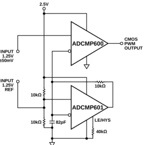
CMOS PWM OUTPUT ADCMP600 2.5V INPUT 1.25V REF INPUT 1.25V ±50mV LE/HYS ADCMP601 82pF 10kΩ 10kΩ 40kΩ 10kΩ 05914-022
Figure 25. Oscillator and Pulse-Width Modulator
ADCMP601 2.5V TO 5V 10kΩ LE/HYS DIGITAL INPUT HYSTERESIS CURRENT 74 AHC 1G07 05914-023
OUTLINE DIMENSIONS
COMPLIANT TO JEDEC STANDARDS MO-203-AA 1.00 0.90 0.70 0.46 0.36 0.26 2.20 2.00 1.80 2.40 2.10 1.80 1.35 1.25 1.15 072809-A 0.10 MAX 1.10 0.80 0.40 0.10 0.22 0.08 3 1 2 4 5 0.65 BSC COPLANARITY 0.10 SEATING PLANE 0.30 0.15
Figure 27. 5-Lead Thin Shrink Small Outline Transistor Package (SC70) (KS-5)
Dimensions shown in millimeters
COMPLIANT TO JEDEC STANDARDS MO-178-AA 10° 5° 0° SEATING PLANE 1.90 BSC 0.95 BSC 0.60 BSC 5 1 2 3 4 3.00 2.90 2.80 3.00 2.80 2.60 1.70 1.60 1.50 1.30 1.15 0.90 0.15 MAX 0.05 MIN 1.45 MAX 0.95 MIN 0.20 MAX 0.08 MIN 0.50 MAX 0.35 MIN 0.55 0.45 0.35 1 1-01-201 0-A
Figure 28. 5-Lead Small Outline Transistor Package (SOT-23) (RJ-5)
1.30 BSC
COMPLIANT TO JEDEC STANDARDS MO-203-AB 1.00 0.90 0.70 0.46 0.36 0.26 2.20 2.00 1.80 2.40 2.10 1.80 1.35 1.25 1.15 072809-A 0.10 MAX 1.10 0.80 0.40 0.10 0.22 0.08 3 1 2 4 6 5 0.65 BSC COPLANARITY 0.10 SEATING PLANE 0.30 0.15
Figure 29. 6-Lead Thin Shrink Small Outline Transistor Package (SC70) (KS-6)
Dimensions shown in millimeters
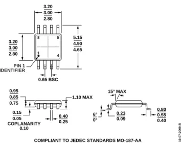
COMPLIANT TO JEDEC STANDARDS MO-187-AA 6° 0° 0.80 0.55 0.40 4 8 1 5 0.65 BSC 0.40 0.25 1.10 MAX 3.20 3.00 2.80 COPLANARITY 0.10 0.23 0.09 3.20 3.00 2.80 5.15 4.90 4.65 PIN 1 IDENTIFIER 15° MAX 0.95 0.85 0.75 0.15 0.05 10-07-20 09-B
Figure 30. 8-Lead Mini Small Outline Package (MSOP) (RM-8)
ORDERING GUIDE
Model1 Temperature Range Package Description Package Option Branding
ADCMP600BRJZ-R2 −40°C to +125°C 5-Lead SOT23 RJ-5 G0C
ADCMP600BRJZ-RL −40°C to +125°C 5-Lead SOT23 RJ-5 G0C
ADCMP600BRJZ-REEL7 −40°C to +125°C 5-Lead SOT23 RJ-5 G0C
ADCMP600BKSZ-R2 −40°C to +125°C 5-Lead SC70 KS-5 G0C ADCMP600BKSZ-RL −40°C to +125°C 5-Lead SC70 KS-5 G0C ADCMP600BKSZ-REEL7 −40°C to +125°C 5-Lead SC70 KS-5 G0C ADCMP601BKSZ-R2 −40°C to +125°C 6-Lead SC70 KS-6 G0N ADCMP601BKSZ-RL −40°C to +125°C 6-Lead SC70 KS-6 G0N ADCMP601BKSZ-REEL7 −40°C to +125°C 6-Lead SC70 KS-6 G0N
ADCMP602BRMZ −40°C to +125°C 8-Lead MSOP RM-8 GF
ADCMP602BRMZ-REEL −40°C to +125°C 8-Lead MSOP RM-8 GF
ADCMP602BRMZ-REEL7 −40°C to +125°C 8-Lead MSOP RM-8 GF
EVAL-ADCMP600BRJZ Evaluation Board
EVAL-ADCMP600BKSZ Evaluation Board
EVAL-ADCMP601BKSZ Evaluation Board
EVAL-ADCMP602BRMZ Evaluation Board
1 Z = RoHS Compliant Part.
©2006–2011 Analog Devices, Inc. All rights reserved. Trademarks and registered trademarks are the property of their respective owners.