3 mm x 3 mm footprint
Description
The A6281 is a 3-channel constant current LED driver that has a wide range of output currents. The A6281 controls LED brightness with a Pulse Width Modulation (PWM) scheme that gives the application the capability of displaying a billion colors in an RGB cluster. The maximum current is set by an external resistor.
The LED brightness is controlled by performing PWM control on the outputs. The brightness data of the PWM signal for each LED is stored in three 10-bit registers. The peak value for each LED can be adjusted (dot-corrected) to compensate for mismatch, aging, and temperature effects. All the internal latched registers are loaded by a 32-bit shift register. One address bit controls whether dot correction/clock divider ratio or brightness data is loaded into the registers. The remaining bits are used for the data.
The A6281 is designed to minimize the number of components needed to drive LEDs with large pixel spacing. A large number of A6281s can be daisy chained together and controlled by just four control signals (clock, serial data, latch, and output enable). Each of these inputs is buffered to drive the next chip in the chain. Also, VIN can be tied to the LED voltage supply
Features and Benefits
▪ 3 × 10-bit PWM brightness settings ▪ 3 × 7-bit dot correction current settings ▪ 5 to 17 V operation▪ Wide output current range, 10 to 150 mA per channel ▪ Internally generated PWM clock
▪ Serial port operates at up to 5 MHz
▪ Data and clock logic architecture allows single microcontroller control of large quantities of serially-connected A6281s at fast data transfer rate
▪ Buffered logic outputs to drive cables ▪ Thermal shutdown and UVLO protection ▪ Power-On Reset
with Programmable PWM Control
Continued on the next page…
Package: 16-terminal QFN (suffix ES)
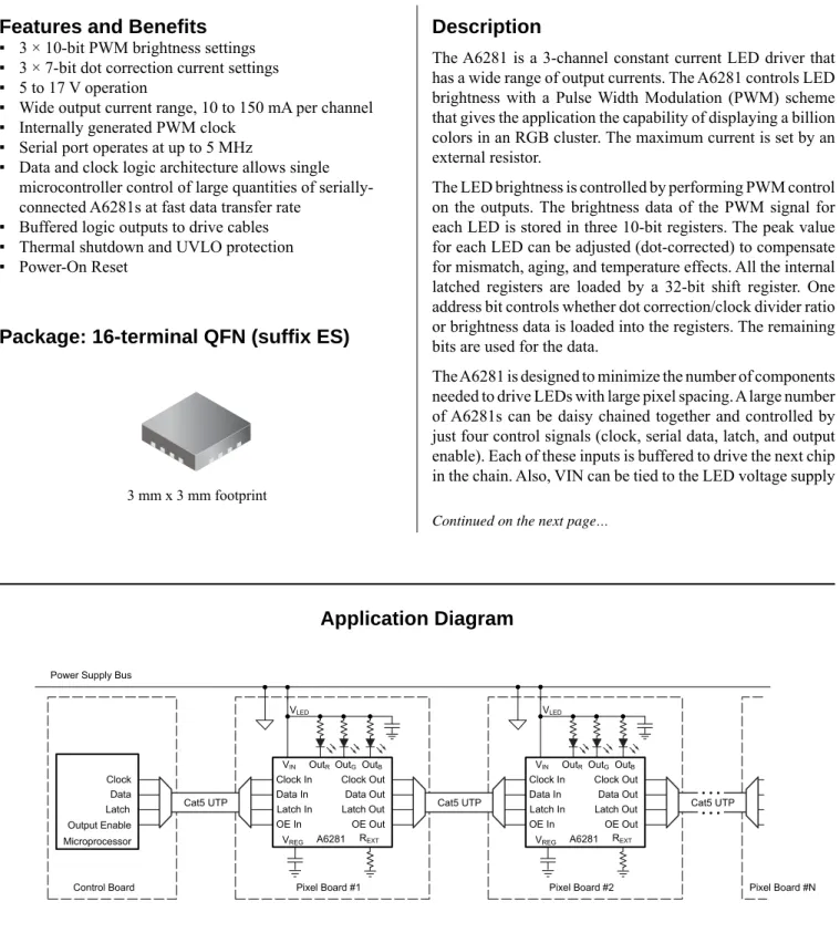
Application Diagram
Figure 1. Functional drawing of daisy chained display application. Additional pixel boards with A6281 ICs can be applied.
Clock Data Output Enable Latch Microprocessor Control Board Clock Out Data Out Latch Out OE Out Clock In Data In Latch In OE In VLED OutB OutG OutR VIN
Power Supply Bus
A6281 Pixel Board #1 REXT VREG Clock Out Data Out OE Out Clock In Data In OE In VLED OutB OutG OutR VIN A6281 Pixel Board #2 REXT VREG Pixel Board #N Latch Out Latch In
bus, thus eliminating the need for a separate chip supply bus or an external regulator.
Applications include:
▪ Colored, large-character LED signs ▪ Scrolling, colored marquees
▪ Architectural lighting
▪ High intensity monochrome displays ▪ Large video and graphic displays
The A6281 is supplied in a 3 mm × 3 mm 16-terminal QFN (suffix ‘ES’) package, with 0.75 mm nominal overall height. The package is lead (Pb) free with 100% matte-tin leadframe plating.
Part Number Packing* Mounting
A6281EESTR-T 1500 pieces/reel 16 terminal QFN
*Contact Allegro for additional packing options.
Selection Guide
Absolute Maximum Ratings
Characteristic Symbol Notes Rating Units
Load Supply Voltage VIN 17 V
Output Voltage VOUT OUT0, OUT1, OUT2 –0.5 to 17 V
Output Current IOUT 170 mA
Ground Current IGND 600 mA
VREG Pin VREG 6 V
Logic Outputs VO CO, LO, OEO, SDO 7 V
Logic Input Voltage Range VI CI, LI, OEI, SDI –0.3 to 7 V
Operating Ambient Temperature TA Range E –40 to 85 ºC
Maximum Junction Temperature TJ(max) 150 ºC
Storage Temperature Tstg –55 to 150 ºC
Description (continued)
Thermal Characteristics
Characteristic Symbol Test Conditions* Rating Units
Package Thermal Resistance RθJA 4-layer PCB based on JEDEC standard 47 ºC/W
*For additional information, refer to the Allegro website.
25 50 75 100 125 150 Temperature (°C) Power Dissipation, P D (mW) 4500 4000 3500 3000 2500 2000 1500 1000 500 0 (R QJA= 47 ºC/W) 4 layer PCB
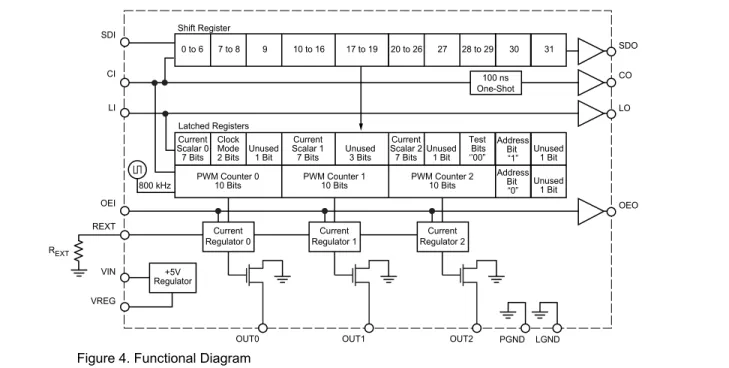
OUT2 OUT1 OUT0 Regulator 800 kHz Clock To PWM Counters To logic To PWM Counters Current Regulator 0 Current Regulator 1 Current Regulator 2 Latched Registers REXT REXT LGND PGND OEO OEI VIN VREG LI LO Shift Register SDI CI SDO CO 100 ns One-Shot
Terminal List Table
Number Name Description
1 REXT An external resistor at this terminal establishes maximum output current
2 VREG Regulator decoupling
3 LGND Logic ground
4 VIN Chip power supply voltage; connect to VREG externally if 4.75 V < VIN < 5.5 V 5 CI Serial clock input; PWM clock if external clock is selected
6 OEI Output enable input; when low (active), the output drivers are enabled; when high (inactive), all output drivers are turned off (blanked)
7 LI Latch input terminal; serial data is latched with high-level input 8 SDI Serial data input to shift register
9 OUT2 Sinking output terminal
10 PGND Power ground
11 OUT1 Sinking output terminal 12 OUT0 Sinking output terminal
13 SDO Buffered serial data output after shift register
14 LO Buffered latch output
15 OEO Buffered output enable output
16 CO Buffered clock output
– PAD Exposed thermal pad, not internally connected; connect externally to LGND and PGND.
Pin-out Drawings Functional Block Diagram
12 11 10 9 1 2 3 4 5 6 7 8 16 15 14 13 CO OEO LO SDO CI OEI LI SDI OUT0 OUT1 PGND OUT2 REXT VREG LGND VIN PAD
OPERATING CHARACTERISTICS, valid at TA = 25°C, VIN = 4.75 to 17.0 V, unless otherwise noted
Characteristic Symbol Test Conditions Min. Typ. Max. Units
ELECTRICAL CHARACTERISTICS
Quiescent Supply Current IDD fCLKIN = 0.0 Hz – – 5.0 mA
Operating Supply Current IDD fCLKIN = 5 MHz – – 15.0 mA
Load Supply Voltage VIN 4.75 – 17 V
Undervoltage Lockout VIN(UV) VIN rising – – 4.5 V
VIN falling 3.0 – – V
VREG Voltage Range1 V
REG IOUT =15 mA, VIN = 17 V 4.6 – 5.4 V
Output Current (any single output) IOUT
REXT = 5 kΩ, scalar = 100% 135 150.0 165 mA
REXT = 15 kΩ, scalar = 100% 45 51 57 mA
Output to Output Matching Error2 Err Output to output variation—all outputs on, R
EXT = 5 kΩ –7 – 7 %
Output Voltage Range VDS(min) 1.0 – 3.0 V
Load Regulation (I%Diff / ∆VDS) REXT = 5 kΩ, VDS = 1 to 3 V – ±1 ±3 %/V
Output Leakage Current IDSX VOH = 17 V – – 1.0 μA
Logic Input Voltage VIH 2.0 – – V
VIL – – 0.8 V
Logic Input Voltage Hysteresis All digital inputs – 150 – mV
CI and SDI Pins Logic Input Current IIN VIN = 0 to 5 V –20 – 20 μA
Input Resistance RI OEI pin, pull-up 150 300 600 kΩ
LI pin, pull-down 100 200 400 kΩ
Logic Output Voltage VOL VIN≥ 5.0 V, IO = ±2 mA – – 0.4 V
VOH 3.8 – – V
Output Dot Correction Error REXT = 5 kΩ; LSB – ±1 – bit
PWM Oscillator fPWM – 800 – kHz
Thermal Shutdown Temperature TJTSD Temperature increasing – 165 – °C
Thermal Shutdown Hysteresis TJhys – 15 – °C
SWITCHING CHARACTERISTICS
Clock Hold Time tH(CLK) 20 – – ns
Data Setup Time tSU(D) 20 – – ns
Data Hold Time tH(D) 20 – – ns
Latch Setup Time3 t
SU(LI) 20 – – ns
Latch Hold Time tH(LI) 20 – – ns
Output Enable Set Up Time tSU(OE) 40 – – ns
Output Enable Falling to Outputs Turning On
Propagation Delay Time tP(OE) – 200 – ns
Clock to Output Propagation Delay Time tP(OUT) External clock selected, VDS = 1.0 V, IO = 150 mA – 200 – ns
Logic Output Fall Time tBF COB = 50 pF, 4.5 to 0.5 V – 50 100 ns
Logic Output Rise Time tBR COB = 50 pF, 0.5 to 4.5 V – 30 60 ns
Output Fall Time (Turn Off) tf COUT = 10 pF, 90% to 10% of IOUT = 10 mA – 10 – ns
COUT = 10 pF, 90% to 10% of IOUT = 150 mA – 10 – ns
Output Rise Time (Turn On) tr COUT = 10 pF, 10% to 90% of IOUT = 10 mA – 50 – ns
COUT = 10 pF, 10% to 90% of IOUT = 150 mA – 100 – ns
Clock Falling Edge to Serial Data Out
Propagation Delay Time tP(SDO) – 50 – ns
Logic In to Output Propagation Delay tP(IO) LI→LO, CI→CO, OEI→OEO – 50 – ns
Clock Out Pulse Duration tw(CLK) 70 100 130 ns
Maximum Clock In Frequency fCI – – 6 MHz
1If V
IN is a 4.75 to 5.5 V supply, connect VIN to VREG externally 2Err = [I
O (min or max) – IO(av)] / IO(av), where IO(av) = average of 3 output current values. 3In daisy-chained applications, t
15 16 31 CI
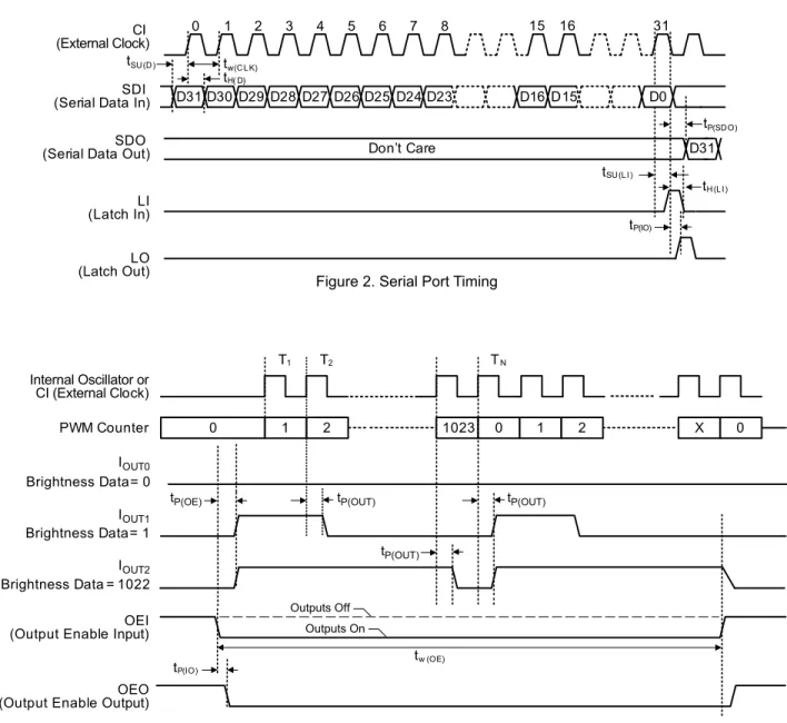
(External Clock) SDI (Serial Data In) SDO (Serial Data Out) LI (Latch In) LO (Latch Out) D31 D29 D28 D27 D26 D25 D24 D23 D16 D15 D0 D31 Don’t Care tw(CLK) tSU(D) tH( D) tP(SDO) tSU(LI) tH(LI) tP(IO) D30 PWM Counter OEI (Output Enable Input)
OEO (Output Enable Output) IOUT0 IOUT1 IOUT2 Brightness Data= 0 Brightness Data= 1 Brightness Data = 1022 tP(IO) t w (OE) tP(OE) tP(OUT) tP(OUT) tP(OUT) Internal Oscillator or CI (External Clock) 0 1 2 1023 0 X 0 T1 T2 TN 1 2 Outputs Off Outputs On 0 1 2 3 4 5 6 7 8
Figure 2. Serial Port Timing
Functional Description
Figure 4. Functional Diagram Shift Register
The A6281 has a 32-bit shift register that loads data through the SDI (serial data in) pin. The shift register operates by a first-in first-out (FIFO) method. The most significant bit (MSB, bit 31) is the first bit shifted in and the least significant bit (LSB, bit 0) is shifted in last. The serial data is clocked by a rising edge of the CI (clock in) pin. The SDO (serial data out) pin is updated to the state of bit 31 on the falling edge of the CI pin. This will prevent any race conditions and erroneous data that might occur while propagating information through multiple A6281s that are daisy chained together. The contents of the shift register will continue to propagate on every rising edge of the CI pin. The information in the shift register is latched on a low-to-high transition of the LI (Latch In) pin. The LI pin must be brought low before the rising edge of the next clock pulse, to avoid latching erroneous data. The latched data remains latched on a rising signal on the OEI (output enable in) pin.
Output Buffers
The A6281 is designed to allow daisy chaining many A6281s together. It can pass the clock, data, latch, and output enable signals from one A6821 to the next without any loss of data due to duty cycle skewing or signal degradation.
The A6821 is equipped with output buffers that allow the data signals to travel over long distances through strings of A6281s without the need for extra driving hardware. The A6281 drives
these signals to TTL levels. Each of the A6281 inputs has a cor-responding buffered output:
• CI (clock in) pin to CO (clock out) pin • LI (latch in) pin to LO (latch out) pin
• OEI (output enable in) pin to OEO (output enable out) pin • SDI (serial data in) pin to SDO (serial data out) pin
The CO (clock out) pin is driven by an internal one-shot circuit. When the CI pin detects an edge rising through the input thresh-old, the one-shot circuitry drives the CO pin high for 100 ns. The CI pin input threshold has hysteresis to prevent false triggering of the CO signal. The implementation of the one-shot solution allows many A6281s to be daisy chained together with a consis-tent clock signal throughout the entire chain without degradation or loss of synchronicity to the data line.
PWM Brightness Control
The A6281 controls the intensity of each LED by pulse width modulating the current of each output. The A6281 has three 10-bit brightness registers, one for each output. These brightness registers set the PWM count value at which the outputs switch off during each PWM cycle. Each 10-bit brightness register gives 1023 levels of light intensity. The duty cycle, DC, can be deter-mined by the following equation:
DC = [(PWMn + 1) / 1024] ×100 (%) ,
where PWMn is the PWM value greater than zero that is stored in the brightness register.
OUT2 OUT1 OUT0 +5V Regulator Current Regulator 0 Current Regulator 1 Current Regulator 2 100 ns One-Shot Shift Register Latched Registers SDI REXT REXT LGND PGND CI SDO CO OEO OEI 800 kHz VIN VREG LI LO 0 to 6 7 to 8 9 10 to 16 17 to 19 20 to 26 27 28 to 29 30 Current Scalar 0 7 Bits Clock Mode 2 Bits Unused1 Bit
Current Scalar 2
7 Bits Unused1 Bit Test Bits ‘’00” Address Bit “1” Address Bit “0” Current Scalar 1
7 Bits Unused3 Bits Unused1 Bit Unused 1 Bit PWM Counter 0
10 Bits PWM Counter 110 Bits PWM Counter 210 Bits
The relationship of the PWMn value to the output duty cycle is given in the following table:
PWMn Duty Cycle 0 0/1024 (0 %) 1 2/1024 2 3/1024 . . . . . . 1023 1024/1024 (100 %)
When the brightness register is set to zero, the outputs remain off for the duration of the PWM cycle for a 0% DC. When a bright-ness register is set to 1023, the LED for that output remains on (100% DC) when OEI is active and begins the PWM cycle. The output remains on when the PWM counter rolls over and begins a new count.
The PWM counter begins counting at zero and increments only when the OEI pin is held low. When the PWM counter reaches the count of 1024, the counter resets to zero and continues incrementing. The counter resets to zero on a rising edge of OEI, upon recovery from UVLO, or when powering up. Latching new data into the brightness registers will not reset the PWM counter. A free-running internal 800 kHz oscillator is the master clock for the PWM counter. A programmable clock divider frequency allows the PWM to be set at approximately at 200 kHz, 400 kHz, or 800 kHz, or the PWM can be set to count on the rising edge of the external CI signal. Bit assignments for the programmable clock divider are shown in the following table:
Bits
Clock Mode
7 8
0 0 800 kHz
1 0 400 kHz
0 1 External (count on rising edge of CI signal)
1 1 200 kHz
The total number of possible colors of an RGB pixel is over 1 billion. Refer to figure 4 for the mapping of shift register bits to latches.
Output Current Selection
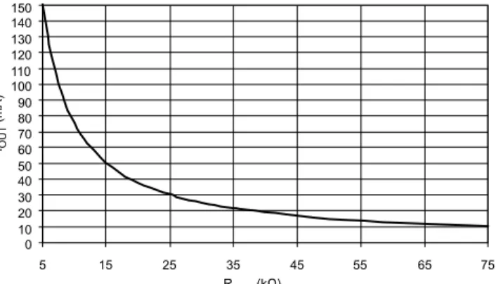
The overall maximum current is set by the external resistor, REXT , connected between the REXT and LGND pins. After being set, the maximum current remains constant regardless of the LED voltage variation, supply voltage variation, temperature, or other circuit parameters. The maximum output current can be calculated using the following equation:
IOUT(max)= 753.12 / REXT.
The relationship of the value selected for REXT and IOUT is shown in figure 6.
Internal Linear Regulator
The A6281 has a built-in linear regulator. The regulator operates from a supply voltage of 5.5 to 17 V. It allows the VIN pin of the A6281 to connect to the same supply as the LEDs. This simpli-fies board design by eliminating the need for a chip supply bus and external voltage regulators. For 5 V supplies, connect VIN to VREG externally. Note: When using 5 V supplies, ensure that VIN does not exceed the absolute maximum rating of the VREG pin (6 V).
The VREGpin is used by the internal linear regulator to connect to a bypass capacitor. This pin is for internal use only and is not
Bits
0 1 2 3 4 5 6 7 8 9 10 11 12 13 14 15 16 17 18 19 20 21 22 23 24 25 26 27 28 29 30a 31
PWM Counter 0 PWM Counter 1 PWM Counter 2 Address “0” Xb
Dot Correction Register 0 Clock Mode X Dot Correction Register 1 X X X Dot Correction
Register 2 X ATBc ATBcAddress “1” X aSelects which word is written to: Dot Correction/Clock Mode selection or PWM counter. bX indicates “Don’t Care.”
cAllegro Test Bit (ATB). Reserved for Allegro internal testing. Always set to zero (0) in the application. Figure 5. Register Configuration
0 10 20 30 40 50 60 70 80 90 100 110 120 130 140 150 5 15 25 35 45 55 65 75 REXT (kΩ) IOUT (mA)
intended as an external power source. There should be a 1.0 μF, 10 V ceramic capacitor connected between the VREG pin and LGND. The capacitor should be located as close to the VREG pin as possible.
Dot Correction Control
The A6281 can further control the maximum output current for each output by setting the three 7-bit dot correction registers with scale data that ranges from 36.5% to 100% of the overall maximum output current that is set by the REXT resistor. This feature is useful because not every type of LED (red, green, or blue, for example) has the same level of brightness for a given current, and the brightness could be different even from LED to LED of the same type. By scaling the output currents so that all the LEDs have matched intensities, the application will have full color depth when using the PWM counters. The dot correction current can be calculated by the following equation:
IOUTn = IOUTn(max) × (Scalen / 2 + 36.5) / 100
Where Scalen is in the range 0 to 127, as shown in the following
table:
Scale
IOUT/IOUT(max)
(%) 0 36.5 1 37.0 2 37.5 . . . . . . 127 100
Refer to figure 5 for the bit configurations for the scalar registers. The dot correction data in the shift register is latched on a rising edge of the LI pin. The dot correction data remains latched on a rising OEI signal. The default output current when the A6281 is powered-up or recovers from a UVLO is 36.5% of the current set by the REXT resistor.
Package Power Dissipation
The maximum allowable package power dissipation is deter-mined as:
PD(max) = (150 – TA) / RθJA .
The actual package power dissipation is:
PD(act) = DC0 × VDS0 × IOUT0
+ DC1 × VDS1 × IOUT1
+ DC2 × VDS2 × IOUT2 + VIN × IIN ,
where DCi is the PWM duty cycle for channel i, and IOUTi is the output current for channel i, determined by the dot correction current for that channel and REXT.
When calculating power dissipation, the total number of avail-able device outputs is usually used for the worst-case situation (3 LEDs at 100% duty cycle).
Thermal Shutdown (TSD)
When the junction temperature of the A6281 reaches the thermal shutdown temperature threshold, TJTSD (165°C typical), the outputs will shut off until the junction temperature cools down below the recovery threshold, TJTSD –∆TJ ( 15°C typical). The shift register and output latches will remain active during the TSD event. Therefore there is no need to reload the data into the output latches.
Undervoltage Lockout
The A6281 includes an internal undervoltage lockout (UVLO) circuit that disables the driver outputs in the event of the logic supply voltage dropping below a minimum acceptable level. This prevents the display of erroneous information, a necessary function for some critical applications. The shift register will not shift any data in a UVLO condition. Upon recovery of the logic supply voltage and on power up, the internal shift register and all latches will be set to zero.
Ballast Resistors
The voltage on the outputs should be kept in the range 1 to 3 V. If the voltage goes below 1V, the current will begin to rolloff as the driver runs out of headroom. At VOUT above 3 V, the power dissipation may become a problem, as each output contributes VOUT × ILED of power loss in the output sink driver. Typically the power supply nominal voltage is chosen to keep the output volt-age in this range. Alternatively, series resistors can be added to dissipate the extra power and keep the output voltage within the recommended range.
Application Information
Timing Considerations
A6281s can be used in large numbers to drive many LEDs with the control signals connected serially together using short cables between each pixel (see figure 8). Because the clock negative edge drives the data to the SDO pin, and the CO pin is driven by a 100 ns one-shot function, the clock and data signals remain synchronized with each other from the first pixel in the chain to the last.
After all of the data is written to each A6281 in the chain, the data is latched into each A6281 via a low-to-high transition on the LI pin. The LO pin of pixel #1 drives the LI pin of pixel #2, and so on down the chain. These signals are buffered and are driven asynchronously relative to the CI and SDI pins. Therefore the mismatch in delays between CO and LO must be taken into consideration.
Although the mismatches in delays are quite small, they must be considered when creating the timing pattern for driving the chain. The key parameter is the setup time from the last CI clock rising edge to the rising edge of LI.
The minimum A6281 setup time from CI to LI is 20 ns. There may be a 5 ns per pixel mismatch in the propagation delays of the CI and LI signals (the delay from CI to CO compared to the delay from LI to LO). As a rule of thumb, use a setup time, tsu , at the first A6281 in the chain as calculated below:
tsu = 20 ns + n × 5 ns , where n is the number of pixels in the chain.
This will ensure that the setup time at the last pixel in the chain is at least 20 ns.
Figure 7. Signal Delay Mismatch Timing Diagram. tsu is the setup time for signals (CI to LI) applied to the first pixel in the chain. Note the difference in delay for CI(1) to CI(n) compared to the delay for LI(1) to LI(n). This must be compensated by increasing tsu.
CO(1) = CI(2) CI(1) CO(2) = CI(3) CO(n-1) = CI(n) LI (1) LO(1) = LI (2) LO(2) = LI (3) LO(n-1) = LI (n) CI(1) to CI(n) tsu LI(1) to LI(n)
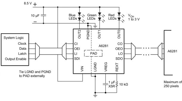
Clock Data Output Enable System Logic CO OEO LO SDO A6281 A6281 Maximum of 250 pixels Latch Clock Data Output Enable System Logic CO OEO LO SDO A6281 A6281 Maximum of 250 pixels Latch Tie LGND and PGND to PAD externally 8.5 V 10 kΩ 1 μF X5R 10 μF VOn 1 to 3 V CI OEI LI PAD SDI Red LEDs Green LEDs Blue LEDs
OUT2 PGND OUT1 OUT0
REXT VREG LGND VIN Tie LGND and PGND to PAD externally VOn 1 to 3 V CI OEI LI PAD SDI
OUT2 PGND OUT1 OUT0
REXT VREG LGND VIN
–
+
–
+
10 V 5 kΩ 1 μF 10 V 10 μF 2 0.5 WΩApplications Drawings
Figure 8. Application driving 3 RGB LED strings, each at 75 mA maximum
ES Package, 16 Pin QFN
C 0.08 17X
A Terminal #1 mark area
B Exposed thermal pad (reference only, terminal #1 identifier appearance at supplier discretion) For reference only
(reference JEDEC MO-220WEED) Dimensions in millimeters
Exact case and lead configuration at supplier discretion within limits shown
C Reference land pattern layout (reference IPC7351 QFN50P300X300X80-17W4M);
All pads a minimum of 0.20 mm from all adjacent pads; adjust as necessary to meet application process requirements and PCB layout tolerances; when mounting on a multilayer PCB, thermal vias at the exposed thermal pad land can improve thermal dissipation (reference EIA/JEDEC Standard JESD51-5)
16 2 1 A 16 1 2
PCB Layout Reference View
B 1.70 1.70 1.70 1.70 0.30 1 16 0.50 0.90 3.10 3.10 C C SEATING PLANE 0.25 +0.05–0.07 0.40 +0.15–0.10 0.50 0.75 ±0.05 3.00 ±0.15 3.00 ±0.15 D
D Coplanarity includes exposed thermal pad and terminals
Copyright ©2006-2008, Allegro MicroSystems, Inc.
The products described here are manufactured under one or more U.S. patents or U.S. patents pending.
Allegro MicroSystems, Inc. reserves the right to make, from time to time, such de par tures from the detail spec i fi ca tions as may be required to per-mit improvements in the per for mance, reliability, or manufacturability of its products. Before placing an order, the user is cautioned to verify that the information being relied upon is current.
Allegro’s products are not to be used in life support devices or systems, if a failure of an Allegro product can reasonably be expected to cause the failure of that life support device or system, or to affect the safety or effectiveness of that device or system.
The in for ma tion in clud ed herein is believed to be ac cu rate and reliable. How ev er, Allegro MicroSystems, Inc. assumes no re spon si bil i ty for its use; nor for any in fringe ment of patents or other rights of third parties which may result from its use.
For the latest version of this document, visit our website: