NCP1650
Power Factor Controller
The NCP1650 is an active, power factor correction controller that can operate over a wide range of input voltages, and output power levels. It is designed to operate on 50/60 Hz power systems. This controller offers several different protection methods to assure safe, reliable operation under any conditions.
The PWM is a fixed frequency, average current mode controller with a wide complement of features. These features allow for both flexibility as well as precision in it’s application to a circuit. Critical components of the internal circuitry are designed for high accuracy, which allows for precise power and current limiting, therefore minimizing the amount of overdesign necessary for the power stage components.
The NCP1650 is designed with a true power limiting circuit that will maintain excellent power factor even in constant power mode. It also contains features that allow for fast transient response to changing load currents and line voltages.
Features
•
Fixed Frequency Operation•
Average Current Mode PWM•
Continuous or Discontinuous Mode Operation•
Fast Line/Load Transient Compensation•
True Power Limiting Circuit•
High Accuracy Multipliers•
Undervoltage Lockout•
Overvoltage Limiting Comparator•
Brown Out Protection•
Ramp Compensation Does Not Affect Oscillator Accuracy•
Operation from 25 to 250 kHz•
This is a Pb−Free DeviceTypical Applications
•
Server Power Converters•
Front End for Distributed Power SystemsDevice Package Shipping†
ORDERING INFORMATION 1 2 3 4 5 6 7 8 16 12 11 10 9 (Top View) AC INPUT Vin Vref AC COMP AC REF FB/SD LOOP COMP PCOMP OUTPUT IS− Iavg−fltr Pmax Iavg 13 RAMP COMP PIN CONNECTIONS 15 14 GND CT
†For information on tape and reel specifications, including part orientation and tape sizes, please refer to our Tape and Reel Packaging Specifications Brochure, BRD8011/D.
www.onsemi.com
NCP1650DR2G SOIC−16 (Pb−Free)
2500/Tape & Reel A = Assembly Location WL = Wafer Lot Y = Year WW = Work Week G = Pb−Free Package MARKING DIAGRAM SO−16 D SUFFIX CASE 751B NCP1650G AWLYWW 1 16 16 1
PIN FUNCTION DESCRIPTION
Pin # Function Description
1 VCC Provides power to the device. This pin is monitored for undervoltage and the unit will not operate if the VCC voltage is not within the UVLO range.
2 Vref 6.5 V regulated reference output. This reference voltage is disabled when the chip is in the shutdown mode.
3 AC
Compensation
Provides pole for the AC Reference Amplifier. This amplifier compares the sum of the AC input voltage and the low frequency component of the input current to the reference signal. The response must be slow enough to filter out most of the high frequency content of the current signal that is injected from the current sense amplifier, but fast enough to cause minimal distortion to the line frequency information. 4 AC REF This pin accommodates a capacitor to ground for filtering and stability of the AC error amplifier. The AC
error amplifier is a transconductance amplifier and is terminated with an internal high impedance load. 5 AC Input The rectified input AC rectified sinewave is connected to this pin. This information is used for the
reference comparator, maximum power circuit, and the average current compensation circuit. 6 Feedback/
Shutdown
The DC output of the converter is reduced through a resistive voltage divider, to a level of 4.0 V, and connected to this pin to provide feedback for the voltage regulation loop. This pin also provides an input undervoltage lockout feature by disabling the chip until the divided output voltage exceeds 0.75 V. It can also be used as a shutdown pin by shorting it to ground with an open collector comparator, or a small signal transistor.
7 Loop
Compensation
A compensation network for the voltage regulation loop, is connected to the output of the voltage error amplifier at this pin.
8 PCOMP A compensation network for the maximum power loop, is connected to the output of the power error amplifier at this pin.
9 PMAX This pin allows the output of the power multiplier to be scaled for the desired maximum power limit level. This multiplier is a proprietary switching design and requires both a resistor and capacitor to ground. The value of this resistor is determined in conjunction with R10.
10 Iavg An external resistor with a low temperature coefficient is connected from this terminal to ground, to set and stabilize the gain of the Current Sense Amplifier output that drives the Power Multiplier and the AC error amplifier. This resistor should be of the same type as that used on pin 9. The value of this resistor will determine the maximum average current that the unit will allow before limiting will occur.
11 Iavgfltr A capacitor connected to this pin filters the high frequency component from the instantaneous current waveform, to create a waveform that resembles the average line current.
12 IS− Negative current sense input. Designed to connect to the negative side of the current shunt.
13 Ramp
Compensation
This pin biases the ramp compensation circuit, to adjust the amount of compensation that is added to the instantaneous current and AC error amp outputs.
14 CT Timing capacitor for the internal oscillator. This capacitor adjusts the oscillator frequency. 15 Ground Ground reference for the circuit.
16 Output Drive output for power FET or IGBT. Capable of driving small devices, or can be connected to an external driver for larger transistors.
MAXIMUM RATINGS (Maximum ratings are those that, if exceeded, may cause damage to the device. Electrical Characteristics are not guaranteed over this range.)
Rating Symbol Value Unit
Power Supply Voltage (Operating) Output (Pin 16) VCC −0.3 to 20 V
Current Sense Inverting Input (Pin 12) V(IS−) −0.5 to 1.0 V
Reference Voltage (Pin 2) Vref −0.3 to 7.5 V
Reference Filter (Pin 4) Ref fltr −0.3 to 5.0 V
All Other Inputs −0.3 to 6.5 V
Thermal Resistance, Junction−to−Air 0.1 in2 Copper 0.5 in2 Copper qJA 130 110 °C/W
Thermal Resistance, Junction−to−Lead (Pin 1) (Note 1) qJL 50 °C/W
Maximum Power Dissipation @ TA = 25°C Pmax 0.77 W
Operating Temperature Range TJ −40 to 125 °C
Non−operating Temperature Range TJ −55 to 150 °C
Stresses exceeding those listed in the Maximum Ratings table may damage the device. If any of these limits are exceeded, device functionality should not be assumed, damage may occur and reliability may be affected.
1. qJL is equivalent to PsiJL
ELECTRICAL CHARACTERISTICS (Unless otherwise noted: VCC = 14 volts, CT = 470 pF, C2 = 0.1 mF, TJ = 25°C for typical values. For min/max values TJ is the applicable junction temperature.)
Characteristic Symbol Min Typ Max Unit
OSCILLATOR
Frequency Fosc 90 100 110 kHz
Max Duty Cycle dmax 0.95 0.97 − −
Min Duty Cycle (Note 2) dmin − 0 5.0 %
Ramp Peak (Note 2) VRpeak − 4.0 − V
Ramp Valley (Note 2) VRvalley − 0.100 − V
Ramp Compensation Peak Voltage (Pin 13) (Note 2) − − 4.0 − V
Ramp Compensation Current (Pin 13) (Note 2) − − 400 − mA
VOLTAGE ERROR AMPLIFIER
Input Bias Current (Note 2) Ibias − 0.2 0.6 mA
Input Offset Voltage (Note 2) VIO − 10 − mV
Transconductance (TJ = −40°C to + 125°C) gm 90 120 150 umho
Output Source (Vref + 0.2 V) IOsource 10 20 − mA
Output Sink (Vref − 0.2 V) IOsink −10 −20 − mA
Boost Current (Vref = 4.0 volts nominal)
Source Boost Current Threshold (Vpin6/Vref) Vfb(boost+) − 1.06 − V/V Sink Boost Current Threshold (Vpin6/Vref) Vfb(boost−) − 0.920 − V/V
Source Boost Current (Vref + 0.4 V) I(boost+) 150 230 − mA
Sink Boost Current (Vref − 0.4 V) I(boost−) −150 −260 − mA
ELECTRICAL CHARACTERISTICS (continued)(Unless otherwise noted: VCC = 14 volts, CT = 470 pF, C2 = 0.1 mF, TJ = 25°C for typical values. For min/max values TJ is the applicable junction temperature.)
Characteristic Symbol Min Typ Max Unit
POWER ERROR AMPLIFIER (Vcomp = 2.0 V, Vref = 2.5 V)
Input Offset Voltage (Note 3) VIO − 20 − mV
Transconductance gm 60 100 150 umho
Output Source (Vref + 0.2 V) IOsource 10 20 − mA
Output Sink (Vref − 0.2 V) IOsink −10 −20 − mA
Boost Current (Vref = 2.5 V nominal)
Source Boost Current Threshold Vfb(boost+) − 1.175 − V/V
Sink Boost Current Threshold Vfb(boost−) − 0.825 − V/V
Source Boost Current (1.3 X Vref) I(boost+) 150 250 − mA
Sink Boost Current I(boost−) −150 −285 − mA
AC ERROR AMPLIFIER
Input Offset Voltage (Note 3) VIO − 20 − mV
Transconductance gm 60 100 150 umho
Output Source (Pin 4 = 4 V, Pin 5 = 0 V) IOsource 25 70 − mA
Output Sink (Pin 4 = 0 V, Pin 5 = 4 V) IOsink −25 −70 − mA
AC Inverting Input Clamp Voltage (250 mA) (TJ = 25°C) Vclamp 4.30 4.45 4.60 V AC Inverting Input Clamp Voltage (250 mA) (TJ = −40°C to +125°C) Vclamp 3.70 − 4.60 V Gain from ACcomp to PWM+ (Av = VPWM+ / (VACcomp – Voffset)) (Note 3) AV − 2.0 − V/V
CURRENT SENSE AMPLIFIER
Input Bias Current (Pin 11) Ibias −40 −50 −80 mA
Differential Input Voltage Range (Note 3) VIdiff − −0.20 − V
Input Offset Voltage VIO 0 2.5 5.0 mV
Output Gain (150 mA/0.150 V) (Voltage Loop Outputs) (Note 3) Av − 1000 − umho Output Gain (150 mA/0.150 V) (Max Pwr Output) (R10 = 15 kW) (Note 3) Av − 1000 − umho
Bandwidth (Note 3) funity − 1.5 − MHz
PWM Output Voltage Gain (k = VPWM+ / Vsense−) (Pin 13 = Open) (TJ = −40°C to + 125°C)
Av 12.9 15 17 V/V
Current Limit Voltage Gain (k = Vace/a / Vsense−) (Vpin5 = 0, R10 = 15 k) Av 13 15 17 V/V Power Output Voltage Gain (k = Vpin10 /Vsense−) (TJ = −40°C to + 125°C) k 13.4 15 17 V/V Current Limit Threshold (Vpin5 = 0, Pin 13 = Open) ILIMthr 225 270 315 mV Current Limit Delay (0 to –450 mV Step) (Note 3) ILIMdelay − 300 − nS
REFERENCE MULTIPLIER
Dynamic Input Voltage Range Ac Input (p−input) (Note 3)
Compensation Input (a−input) (Note 3) Offset Voltage (a−input)
Vmax − − − 3.75 − 1.0 − − − V Multiplier Gain (Note 3) k+ Vmult out
(VACńVramp pk) (VLOOPcomp*Voffset)
k − 8.0 − 1.0/V
ELECTRICAL CHARACTERISTICS (continued)(Unless otherwise noted: VCC = 14 volts, CT = 470 pF, C2 = 0.1 mF, TJ = 25°C for typical values. For min/max values TJ is the applicable junction temperature.)
Characteristic Symbol Min Typ Max Unit
MAXIMUM POWER MULTIPLIER
Multiplier Gain (TJ = 25°C) (TJ = −40°C to +125°C) R9 = 47 k, R10 = 15 k K+ Vpin9 (−Vpin12) Vpin5[ 4.0 R9 R10 k 12.1 11.8 12.8 12.8 13.3 13.3 1.0/V
Dynamic Input Voltage Range
Ac Input (p−input) (Note 4) Vmax − 3.75 − V
AC INPUT (Pin 5)
Input Bias Current
(Total bias current for both multipliers and current compensation amplifier)
IINbias − 0.01 − mA
DRIVE OUTPUT
Source Resistance (80 mA Load) Rsource 4.0 8.0 15 W
Sink Resistance (−80 mA Load) Rsink 3.0 8.0 15 W
Rise Time (CL = 1.0 nF, 20% to 80%) tr − 50 − ns
Fall Time (CL = 1.0 nF, 20% to 80%) tf − 50 − ns
Output Voltage in UVLO Condition VO(UV) − 1.0 10 mV
VOLTAGE REFERENCE
4.0 Volt Reference (Pin 6) (TJ = 25°C) Vref 3.94 4.00 4.06 V
4.0 Volt Regulation (TJ = −55°C to 125°C) Vref 3.92 4.00 4.08 V
2.5 Volt Reference (Pmax, Pin 9) Vref2.5 2.40 2.50 2.60 V
Buffered Output (Iload = 0 mA) VrefOUT 6.24 6.50 6.76 V
Load Regulation (Buffered Output, Io = 0 to 10 mA, VCC > 10 V) DVrefOUT 0 4.0 40 mV
UNDERVOLTAGE LOCKOUT/SHUTDOWN
UVLO Startup Threshold (VCC Increasing) VSU 10 10.5 11 V
UVLO Hysteresis (Shutdown Voltage = VSU – VH) VH 0.3 0.5 0.7 V Shutdown Startup Threshold (Pin 6) (Vout Increasing) VSD 0.50 0.85 1.00 V
Shutdown Hysteresis (Pin 6) VH 0.10 0.18 0.3 V
OVERVOLTAGE PROTECTION
Overvoltage Voltage Trip Point (Vpin6/Vref) VOV 106.5 108 109.5 V/V Overvoltage Voltage Differential (VOV − Vboost+) VOVdiff − 50 − mV
TOTAL DEVICE
Operational Bias Current (CL(Driver) = 1.0 nF, 100 kHz) IBIAS − 4.0 5.0 mA
Bias Current in Undervoltage Mode IBshutdown − 0.6 1.0 mA
REFERENCE REGULATOR UVLO -+ SHUTDOWN 0.85 V REFERENCE MULTIPLIER CURRENT SHAPING NETWORK CURRENT SENSE AMPLIFIER RAMP COMP CT IS− OUT VCC FB/SD AC INPUT GND
Figure 1. Simplified Block Diagram -+ OVERVOLTAGE COMPARATOR 1.08 Vref POWER MULTIPLIER -+ POWER AMP LOOP COMP -+ ERROR AMP VOLTAGE/POWER ORing NETWORK 4 V PCOMP 2.5 V + − OSCILLATOR CONTROL LOGIC 20 mA -+ 200 mA 4.24 V -+ 200 mA 3.68 V
OSCILLATOR BLANKING PULSE OSCILLATOR RAMP GND 4 V LATCH Q DRIVE OVERVOLTAGE COMPARATOR UVLO or SHUTDOWN PWM
Figure 2. Timing Diagram AC Error Amp + Ramp Comp + Inductor Current
Typical Performance Characteristics
(Test circuits are located in the document TND307/D)
600 200
100 0
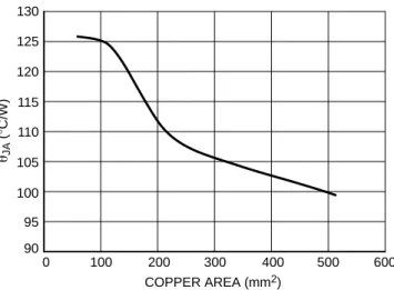
Figure 3. qJA as a Function of the Pad Copper Area (1 oz. Cu Thickness) for a JEDEC Test PCB
COPPER AREA (mm2) 130 110 95 90 qJA ( ° C/W) 400 300 500 100 105 125 115 120
Typical Performance Characteristics
(Test circuits are located in the document TND307/D)
1000 100
10 1.0
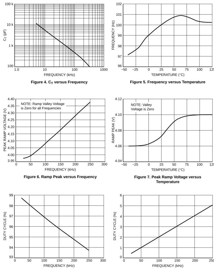
Figure 4. CT versus Frequency FREQUENCY (kHz) 100 k 10 k 1 k 100 CT (pF) 25 0 −25 −50
Figure 5. Frequency versus Temperature TEMPERATURE (°C) 102 99 98 96 FREQUENCY (Hz) 50 75 100 125 97 101 100 300 200 250 150 100 50 0
Figure 6. Ramp Peak versus Frequency FREQUENCY (kHz)
4.05 4.00 3.95
PEAK RAMP VOL
T AGE (V) 4.15 4.10 4.25 4.20 4.35 4.30 4.40
NOTE: Ramp Valley Voltage is Zero for all Frequencies
25 0 −25 −50
Figure 7. Peak Ramp Voltage versus Temperature TEMPERATURE (°C) 4.12 4.08 4.04 RAMP PEAK (V) 50 75 100 125 4.06 4.10 NOTE: Valley Voltage is Zero 300 200 250 150 100 50 0
Figure 8. Max Duty Cycle versus Frequency FREQUENCY (kHz) 94 93 DUTY CYCLE (%) 95 96 98 97 99 250 200 150 100 0
Figure 9. Minimum Duty Cycle versus Frequency FREQUENCY (kHz) 2 0 DUTY CYCLE (%) 3 4 5 6 1 50
Typical Performance Characteristics
(Test circuits are located in the document TND307/D)
0.6 0.2 0.4
−0.2 0
−0.4 −0.6
Figure 10. Voltage Amplifier Gain PIN 6 VOLTAGE RELATIVE TO 4.0 V REF−BOOST CIRCUIT 300 200 100 0 −100 −200 −300 OUTPUT CURRENT ( m A) 0.3 0.1 0.2 −0.1 0 −0.2 −0.3
Figure 11. Voltage Amplifier Gain
PIN 6 VOLTAGE RELATIVE TO 4.0 V REF−LINEAR REGION 30 20 10 0 −10 −20 −30 OUTPUT CURRENT ( m A) 1.5 0.5 1.0 −0.5 0 −1.0 −1.5
Figure 12. Power Amplifier Gain
PIN 9 VOLTAGE RELATIVE TO 2.5 V REF−BOOST CIRCUIT 400 200 100 0 −100 −200 −300 OUTPUT CURRENT ( m A) 0.6 0.2 0.4 −0.2 0 −0.4 −0.6
Figure 13. Power Amplifier Gain
PIN 9 VOLTAGE RELATIVE TO 2.5 V REF−LINEAR REGION 40 20 10 0 −10 −20 −50 OUTPUT CURRENT ( m A) 300 30 −30 −40 350 150 200 100 50 0
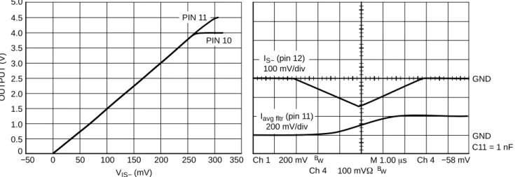
Figure 14. Current Sense Amplifier Gain VIS− (mV) 5.0 2.5 0 OUTPUT (V) 250 300 −50 0.5 1.0 1.5 2.0 4.5 3.0 3.5 4.0 PIN 10 PIN 11
Figure 15. Current Sense Amplifier High Frequency Response GND GND IS− (pin 12) 100 mV/div Iavg fltr (pin 11) 200 mV/div −58 mV 200 mV C11 = 1 nF M 1.00 ms Ch 1 Ch 4 100 mVW Ch 4 BW BW
Typical Performance Characteristics
(Test circuits are located in the document TND307/D)
5.0
3.0 4.0
2.0 1.0
0
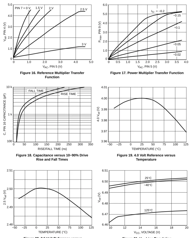
Figure 16. Reference Multiplier Transfer Function VAC, PIN 5 (V) 5.0 4.0 3.0 2.0 1.0 0 Vref , PIN 4 (V) PIN 7 = 0 V 1.5 V 2 V 2.5 V 3 V 4.0 3.0 3.5 2.5 1.5 2.0 1.0 0.5 0
Figure 17. Power Multiplier Transfer Function VAC, PIN 5 (V) 6.0 5.0 4.0 3.0 2.0 1.0 0 Pmax , PIN 9 (V) IS− = −0.2 −0.15 −0.1 −0.05 −0.02 350 150 200 100 50 0
Figure 18. Capacitance versus 10−90% Drive Rise and Fall Times
RISE/FALL TIME (ns) 10 k 1 k 100 C, PIN 16 CAP ACIT ANCE (pF) 250 300 FALL TIME RISE TIME 125 25 0 −50
Figure 19. 4.0 Volt Reference versus Temperature TEMPERATURE (°C) 3.97 3.96 4.0 V ref (V) 3.99 4.00 4.01 −25 3.98 100 75 50 125 75 100 50 25 −50
Figure 20. 2.5 Volt Reference versus Temperature TEMPERATURE (°C) 2.49 2.48 2.5 V ref (V) 2.50 2.51 −25 0 10 14 16 20
Figure 21. Vref Line Regulation VCC, VOLTAGE (V) 6.47 6.46 Vref (V) 6.48 6.50 6.51 12 −40°C 25°C 125°C 18 6.49
Typical Performance Characteristics
(Test circuits are located in the document TND307/D)
10 8
6 4
0
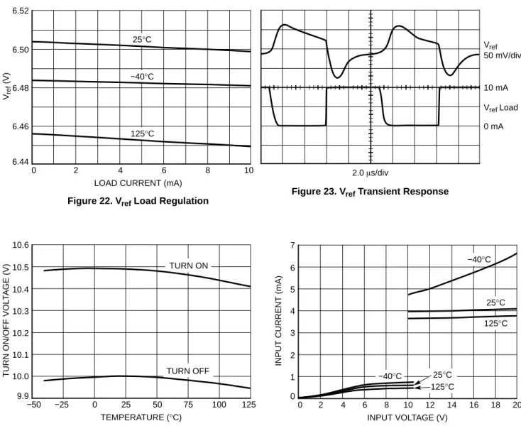
Figure 22. Vref Load Regulation LOAD CURRENT (mA) 6.46 6.44 Vref (V)6.48 6.50 6.52 2 −40°C 25°C 125°C
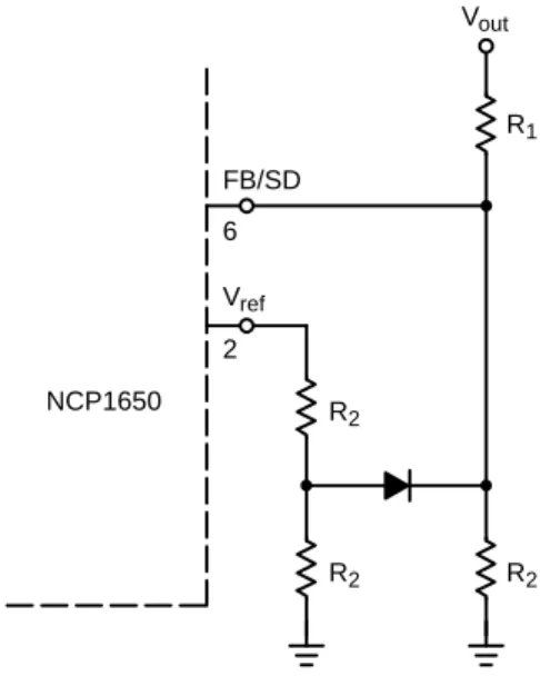
Figure 23. Vref Transient Response 2.0 ms/div 0 mA 10 mA 50 mV/div Vref Vref Load 125 75 100 50 25 −50
Figure 24. UVLO versus Temperature TEMPERATURE (°C)
10.1
9.9
TURN ON/OFF VOL
T AGE (V) 10.2 10.3 10.5 10.4 10.6 10.0 −25 0 TURN ON TURN OFF 20 10 12 8 6 0
Figure 25. Input Current versus Input Voltage INPUT VOLTAGE (V)
1 0
INPUT CURRENT (mA)
5 7 2 4 14 16 2 3 4 6 −40°C 25°C 125°C −40°C 25°C 125°C 18
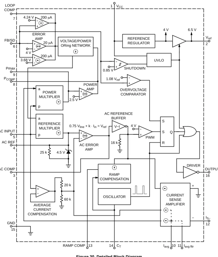
Figure 26. Shutdown Override Circuit R2 R2 R2 R1 NCP1650 FB/SD Vref 6 2 Vout RESISTOR−DIODE NETWORK
Figure 27. Shutdown Override Circuit R2 R1 NCP1650 FB/SD Vref 6 2 Vout ZENER DIODE 4.7 V
(This circuit will not override the shutdown until the chip has achieved it’s initial enable state)
Figure 28. External Shutdown Circuit
R2 4.7 k R1 NCP1650 FB/SD 6 Vout
Figure 29. Soft−Start Circuit 20 k 5 V − Shutdown 0 V − Normal Operation 2N3904 R3 0.33 mF NCP1650 3 33 k AC COMP Vref 2 C3 BAS16LT1 MMBT2907AL
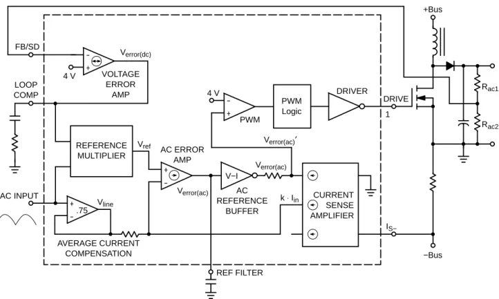
REFERENCE REGULATOR UVLO -+ SHUTDOWN 4 V 6.5 V -+ -+ 0.85 V REFERENCE MULTIPLIER V−I AC REFERENCE BUFFER 4 V 0.75 Vline + k ⋅ Iin = Vref 4.5 V 25 k AC ERROR AMP 16 k PWM Q S R DRIVER -+ AVERAGE CURRENT COMPENSATION 20 k 60 k RAMP COMPENSATION OSCILLATOR CURRENT SENSE AMPLIFIER
RAMP COMP 13 14 CT Iavg 10 11 Iavg fltr
IS− OUTPUT 16 12 Vref 2 1 VCC FB/SD 6 AC INPUT 5 AC REF 4 GND 15 AC COMP 3 a p
Figure 30. Detailed Block Diagram -+ OVERVOLTAGE COMPARATOR S POWER MULTIPLIER a p -+ POWER AMP LOOP COMP 7 -+ ERROR AMP VOLTAGE/POWER ORing NETWORK 4 V Pmax 9 2.5 V PCOMP 8 + − 1.08 Vref -+ 200 mA 4.24 V 20 mA -+ 3.68 V 200 mA
THEORY OF OPERATION Introduction
Optimizing the power factor of units operating off of AC lines is becoming more and more important. There are a number of reasons for this.
There are a growing number of government regulations requiring Power Factor Correction (PFC). Many of these are originating in Europe. Regulations such as IEC1000−3−2 are forcing equipment to utilize input stages with topologies other than a simple off−line front end which contains a bridge rectifier and capacitor.
There are also system requirements that dictate the use of PFC. In order to obtain the maximum power from an existing circuit in a building, the power factor is very critical. The real power available from such a circuit is:
Preal+Vrms Irms PF
A typical off−line converter will have a power factor of 0.5 to 0.6, which means that for a given circuit breaker rating only 50% to 60% of the maximum power is available. If the power factor is increased to unity, the maximum available power can be obtained.
There is a similar situation in aircraft systems, where a limited supply of power is available from the on−board generators. Increasing the power factor will increase the load on the aircraft without the need for a larger generator.
Figure 31. Voltage and Current Waveforms v, i v, i OFF−LINE CONVERTER PFC CONVERTER t t V V I I
Unity power factor is defined as the current waveform being in phase with the voltage, and undistorted. Therefore, there are two causes of power factor degradation – phase shift and distortion. Phase shift is normally caused by reactive loads such as motors which are inductive, or electroluminescent lighting which is highly capacitive. In such a case the power factor is relatively simple to analyze, and is determined by the phase shift.
PF+cosq
Where q is the phase angle between the voltage and the current.
Reduced power factor due to distortion is more complicated to analyze and is normally measured with AC analyzers, although most circuit simulation programs can also calculate power factor. One of the major causes of distortion is rectification of the line into a capacitive filter. This causes current spikes that do not follow the input voltage waveform. An example of this type of waveform is shown in the upper diagram in Figure 2.
A power converter with PFC forces the current to follow the input waveform. This reduces the peak current, the rms current and eliminates any phase shift.
The NCP1650 accomplishes this for both continuous and discontinuous mode power converters.
PFC Operation
The basic PWM function of the NCP1650 is controlled by a small block of circuitry, which comprises the DC regulation loop and the PFC circuit. These components are shown in Figure 26.
There are three inputs to this loop. They are the fullwave rectified input sinewave, the instantaneous input current and the DC output voltage.
The input current is forced to maintain a near unity power factor due to the control of the AC error amplifier. This amplifier uses information from the AC input voltage and the AC input current to control the power switch in a manner that provides good DC regulation as well as an excellent power factor.
The reference multiplier sets a reference level for the input fullwave rectified sinewave waveform. One of its inputs is connected to the scaled down fullwave rectified sinewave, and the other is connected to the output of the DC error amplifier. The signal from the DC error amplifier adjusts the level of the fullwave rectified sinewave on its output without distorting it. To accomplish this, it is necessary for the bandwidth of the DC error amp to be less than twice the lowest line frequency. Typically it is set at a factor of ten less than the rectified frequency (e.g. for a 60 Hz input, the bandwidth would be 12 Hz).
Figure 32. Simplified Block Diagram of Basic PFC Control Circuit + -+ REFERENCE MULTIPLIER AC REFERENCE BUFFER Vref AC ERROR AMP PWM DRIVER AVERAGE CURRENT COMPENSATION CURRENT SENSE AMPLIFIER DRIVE 1 AC INPUT .75 PWM Logic LOOP COMP Vline V−I REF FILTER 4 V +Bus Verror(ac)′ Verror(ac) FB/SD -+ 4 V IS− Verror(ac) VOLTAGE ERROR AMP −Bus Rac1 Rac2 Verror(dc) k ⋅ Iin +
-The key to understanding how the input current is shaped into a high quality sine wave is the operation of the AC error amplifier. The inputs of an operational amplifier operating in its linear range, must be equal.
There are several secondary effects, that create small differences between the inverting and non−inverting inputs, but for the purpose of this analysis they can be considered to be equal.
The fullwave rectified sinewave output of the reference multiplier is fed into the non−inverting input of the AC error amplifier. The inverting input to the AC error amplifier receives a signal that is comprised of the input fullwave rectified sinewave (which is not modified by the reference multiplier), and summed with the filtered input current. Since the two inputs to this amplifier will be at the same potential, the complex signal at the inverting input will have the same wave shape as the AC reference signal. The AC reference signal (Vref) is a fullwave rectified sinewave, and the AC input signal (Vline) is also a fullwave rectified sinewave, therefore, the AC current signal (Iin), must also be a fullwave rectified sinewave. This relationship gives the formula:
Vref+.75 · Vline)(k · Iin)
The Iin signal has a wide bandwidth, and its instantaneous value will not follow the low frequency fullwave rectified sinewave exactly, however, the output of the AC error amplifier has a low frequency pole that allows the average value of the .75 Vline + (k x Iin) to follow Vref. Since the AC error amplifier is a transconductance amplifier, it is followed by an inverting unity gain buffer stage with a low impedance
output so that the signal can be summed with the instantaneous input switching current (Iin). The output of the buffer is still Verrorac.
Figure 33. Typical Signals for PFC Circuit AC Input Vref Vline k ⋅ Iin Vline + k ⋅ Iin Verror(ac) Verror(ac)′ Verror(ac) Vref OSC 4 V ref GND GND 4 V ref
The difference between Verror(ac) and the 4.0 volt reference, sets the window that the instantaneous current will modulate in, to determine when to turn the power switch off.
The switch is turned on by the oscillator, which makes this a fixed frequency controller. Under normal operation, the switch will remain on until the instantaneous value of Verror(ac)′ reaches the 4.0 volt reference level, at which time the switch will turn off.
Since the input current has a fundamental frequency that is twice that of the line, the output filter must have poles lower than the input current to create a reasonable DC waveform. The output DC voltage is divided down via. an external divider and fed back to the DC error amplifier.
Protection Features
The NCP1650 contains a number of features to protect the device and circuit from overload and stressful conditions. These include:
•
Output voltage overshoot protection•
Low line input protection•
Instantaneous current limit•
Line frequency current limit•
Maximum power limitOutput Voltage Overshoot Protection
An overshoot comparator has been provided to monitor the output voltage. Due to the slow transient response of a PFC controller, a fast load dump can cause a large output voltage transient to occur.
The overshoot comparator uses the same input as the feedback and shutdown signals. Its reference is set 8% higher than the reference used by the error amplifier. This comparator will shutdown the output stage if the output voltage exceeds the set level by 8%. The circuit will resume operation once the voltage is reduced to within 8% of the set level.
Low Line Input Protection
This feature uses the shutdown circuitry to assure that the unit does not start under low line condition. PFC converters typically are designed with an output voltage of 400 VDC. To reduce this to the level of the 4.0 volt reference, a 100:1 ratio is required for the voltage divider to the FB/SD pin. When the converter is energized, the output voltage will be the peak line voltage. If the peak line voltage does not exceed 75 volts (0.75 volts at the FB/SD pin) the unit will not start. This corresponds to a line voltage of 53 volts rms. Application circuits have been provided in Figures 33 and 34 to override this feature if desired.
Instantaneous Current Limit
The fastest protection available is a cycle−by−cycle current limit feature.
The current sense amplifier has three outputs. One is the instantaneous current in the inductor, and the other two are average current waveforms. The instantaneous current signal goes directly to the PWM and is terminated by an internal 16 kW resistor. This current signal is added to the output of the AC error amplifier and the ramp compensation signal. The switch will conduct current until the sum of these three signals reaches the 4.0 V reference of the inverting input to the PWM comparator. The peak current is determined by the value of the ramp compensation resistor (R13) and the current shunt.
Line Frequency Current Limit
The output of the reference multiplier determines the current that will be required for the unit to regulate. The sum of the input voltage from the Average Current Compensation amplifier and the averaged current signal from the current sense amplifier must add to the level of the reference multiplier. The output of this multiplier is clamped to a 4.5 maximum level. The maximum average current is set by R10.
This form of protection is slower than the cycle−by−cycle current limiting, but faster than the maximum power limit circuit.
Maximum Power Limit
The NCP1650 can limit the output power to protect against nuisance tripping of circuit breakers or other input power restrictions. It should be understood that boost regulators by design, can not be short circuit limited. Operation of the power limiting circuit will reduce the output voltage only to the level where it is equal to the peak of the input line voltage. At this point, the rectified line voltage will continue to provide output voltage through line frequency rectification by means of the series rectifier diode.
The input power of the converter is calculated by the power multiplier. By multiplying the instantaneous input voltage (AC input signal, pin 5) and the instantaneous input current (averaged current sense amplifier output), the actual input power is accurately calculated.
The power multiplier has a very low frequency pole which converts the power to a filtered DC level. The power error amplifier has a reference set at 2.5 volts. If the output of the power multiplier reaches 2.5 volts, the power error amplifier takes control of the loop via the ORing network and will regulate a constant power output within the limits of the power stage. It should be understood that once the output voltage is reduced to a level equal to the peak of the input voltage, the converter can no longer control the output power.
The output power level is set by combination of the Iavg resistor at pin 10 and the Pmax resistor at pin 9.
OPERATING DESCRIPTION DC Reference and Buffer
The internal DC reference is a precision bandgap design with a nominal output voltage of 4.0 volts. It is temperature compensated, and trimmed for a $1% tolerance of its nominal voltage, with an overall tolerance over line and temperature of $2%. To assure maximum stability, this is only used as a reference so there is minimal loading on this source.
The DC reference is fed into a buffer with a gain of 1.625 which creates a 6.5 volt supply. This is used as an internal voltage to power many of the blocks inside of the NCP1650 and is also available for external use. The 6.5 volt reference is designed to be terminated with at 0.1 mF capacitor for stability reasons.
There is no buffer between the internal and external 6.5 V supply, so care should be used when connecting external loads. A short or overload on this voltage output will inhibit the operation of the chip.
There is also a 2.5 volt reference on the power amplifier. This is derived by a resistive voltage divider off of the 4.0 V reference.
Undervoltage Lockout
An Undervoltage Lockout circuit (UVLO) is provided to assure that the unit does not exhibit undesirable behavior at low Vcc levels. It also reduces power consumption to a level that allows rapid charging of the Vcc cap.
When the Vcc cap is originally charging, the UVLO will hold the unit off, and in a low bias current mode until the Vcc voltage reaches a nominal 10.5 volt level. At this point the unit will begin operation, and the UVLO will no longer be active. If the Vcc voltage falls to a level that is 0.5 volts below the turn−on point, the UVLO circuit will again become active.
When in the shutdown state, the UVLO circuit removes power from all internal circuitry by shutting off the 6.5 volt supply. The 4.0 volt reference remains active, and the UVLO and Shutdown comparators are also active.
Multipliers
The NCP1650 uses a new proprietary concept for the Power and Reference multipliers. This innovative design allows greatly improved accuracy compared to a conventional linear analog multiplier. The multipliers use a PWM switching circuit to create a scalable output signal, with a very well defined gain.
One input (A) to the multiplier is a voltage−to−current (V−I) converter. By converting the input voltage into a current, an overall multiplier gain can be accomplished. In addition, there will be no error in the output signal due to the series rectifier.
The other signal (Input P) is inputted into the PWM comparator. This selects a pulse width for the comparator output. The current signal from the V−I converter is factored by the duty cycle of the PWM comparator, and then filtered
by the RC network on the output. This network creates a low pass filter, and removes the high frequency content from the original waveform.
Figure 34. Simplified Multiplier Schematic INPUT A INPUT P RAMP OUTPUT Inverting Input NI Input V to I CONVERTER -+
The multiplier ramp is generated by the internal oscillator, and is the same signal as is used in the PWM. It will therefore have the same frequency as the power stage.
It is not necessary for Input P (into the PWM comparator) to be a DC signal, low frequency AC signals (relative to the ramp frequency) work well also.
The gain of the multiplier is determined by the current−to−voltage ratio of the V−I converter, the load resistor of the output filter and the peak and valley points of the sawtooth ramp. When the P input signal is at the peak of the ramp waveform, the comparator will allow the A input signal to pass without chopping it at all. This gives an output voltage of the A current multiplied by the output filter resistance. When the P input signal is at the ramp valley voltage, the comparator is held low and no current is passed into the output filter. Between these two extremes, the duty cycle (and therefore, the output signal) is proportional to the level of the P input signal.
The output filter is a parallel RC network. The pole for this network needs to be greater than twice the highest line frequency (120 Hz for a 60 Hz line), and less than the switching frequency.
Reference Multiplier The two multipliers have different rules for designing their filters. The reference multiplier contains an internal loading resistor, with a nominal value of 25 kW. This is because the resistor that converts the A input voltage into a current is internal. Making both of these resistors internal, allows for good accuracy and good temperature performance. Only a capacitor needs to added externally to properly compensate this multiplier. It is not
recommended that an external resistor be used at the “Ref Gain” pin, due to tolerance variations of the internal resistances.
The voltage−to−current conversion is performed in the Voltage/Power ORing network. This circuit also limits the maximum input signal (from the error amplifier) to 3 volts. Power Multiplier/Current Sense Amplifier There is no voltage−to−current converter on the power multiplier. The current output of the current sense amplifier is used for the analog input with no scaling.
The power multiplier requires an external resistor as well as an external capacitor. The value of the resistor at pin 9 (max power) will depend on the value of the resistor used at pin 10 for the current gain and the maximum desired output power of the converter. These resistors should be the same style of resistor and have the same temperature coefficients for best performance.
The gain of the power multiplier is based on the values of external components on this multiplier as well as the current sense amplifier. The current sense amplifier output that drives the power multiplier has its gain controlled by R9 and R10, and is filtered by a capacitor on pin 11 which removes the high frequency content from the inductor current signal. The gain for the power multiplier can be calculated as follows:
(1.) V9+ICS R9 (VacńVramp)
Where:
ICS is the rms value of the average current out of the current sense amplifier
R9 is the resistor value at pin 9 (Ohms) Vac is the rms voltage at pin 5
Vramp is the sawtooth p−p ramp voltage (4.0 volts) and,
(2.) ICS+VCS 15ńR10
Since the pole at pin 12 is much greater than twice the line frequency we can ignore the effects of the capacitor on this pin. VCS is the differential current sense rms input voltage. Equations 1 and 2 can be rearranged to give the gain of the multiplier:
(3.) V9+3.75@R9@VCS@Vac R10
This gain equation gives the output voltage of the multiplier, where the inputs are the AC fullwave rectified sinewave and the current sense input signal.
Figure 35. Reference Multiplier Clamp Circuit
25 k AC Error Amplifier Multiplier 1 k 4.5 V AC Ref -+
There is a 1 k resistor between the AC Ref pin and the AC Error Amplifier for ESD protection. Due to this resistor, the voltage on pin 4 will exceed 4.5 volts under some conditions, but the maximum voltage at the non−inverting AC Error Amplifier input will be clamped at 4.5 volts.
Feedback/Shutdown
The FB/SD pin is a multiple function pin. Its primary function is to provide an input to the error amplifier for sensing of the output voltage. The signal at this pin is also sensed by an internal comparator that will shutdown the unit if the voltage falls below 0.75 volts.
The feedback circuit applies the signal to the non−inverting input of the voltage loop error amp. The other input of the error amp is connected to the internal 4.0 volt reference. The output of a voltage divider from the high voltage DC output to ground, feeds this pin.
The shutdown function can be used for multiple purposes including overvoltage, undervoltage or hot−swap control. An external transistor, open collector or open drain gate, connected to this pin can be used to pull it low, which will inhibit the operation of the chip, and change the operating state to a low power standby mode. An example of a shutdown circuit is shown in Figure 36.
The shutdown circuit is designed such that under normal line conditions the unit will be on. At startup, the AC line is rectified and charges up the output capacitor. Under normal line conditions, the output voltage will be great enough to apply more than 1.0 volt to this pin and the circuit will commence switching. If the unit is turned on into a low line condition, the voltage at this pin will not allow the unit to start.
Figures 33 and 34 shown circuits that can be used to disable the shutdown function. Both of these circuits limit the minimum voltage that can appear at the FB/SD input when the chip is properly biased, while not interfering with the 4.0 volt level that pin 6 sees when the unit is operating properly.
Ramp Compensation
The Ramp Compensation pin allows the amount of ramp compensation to be adjusted for optimum performance. Ramp compensation is necessary in a current mode
converter to stabilize the units operation when the duty cycle is greater than 50%.
The amount of compensation required is dependent on several variables, including the boost inductor value, and the desires of the designer. The value should be based on the falling di/dt of the inductor current. For a boost inductor with a variable input voltage, this will vary over the AC input cycle, and with changes in the input line. A di/dt chart is included in the design spreadsheet that is available for the NCP1650.
This pin is a buffered output of the oscillator, which provides a voltage equal to the ramp on the oscillator CT pin. A resistor from this pin to ground, programs a current that is transformed via a current mirror to the non−inverting input of the PWM comparator.
The ramp voltage due to the inductor di/dt at the input to the PWM comparator is the current shunt voltage at pin 11 multiplied by 15, which is the gain of the current amplifier output that feeds the PWM.
Figure 36. Ramp Compensation Circuit -+ Oscillator -+ 16 k AC Ref Buffer Current Sense Amp PWM Comparator 13 Ramp Compensation 1.6i i RRC
The current mirror is designed with a 1:1.6 current ratio. The ramp signal injected can be calculated by the following formula:
VRcomp+1.6 Voscpk 16 kRRC +RRC102
Where:
VRcomp = Peak injected ramp signal (v) RRC = Ramp compensation resistor (kW)
Oscillator
The oscillator generates the sawtooth ramp signal that sets the switching frequency, as well as sets the gain for the multipliers. Both the frequency and the peak−to−peak amplitude are important parameters.
The oscillator uses a current source for charging the capacitor on the CT pin. The charge rate is approximately 200 mA and is trimmed to maintain an accurate, repeatable frequency. Discharge is accomplished by grounding the CT
pin with a saturated transistor. A hysteretic comparator monitors that ramp signal and is used to switch between the current source and discharge transistor. While the cap is charging, the comparator has a reference voltage of 4.0 volts. When the ramp reaches that voltage, the comparator switches from the charging circuit to the discharge circuit, and its reference changes from 4.0 to X0.5 volts (overshoot and delays will allow the valley voltage to reach 0 volts).
The relationship between the frequency and timing capacitor is:
CT+47, 000ńf
Where CT is in pF and f is in kHz.
It is important not to load the capacitor on this pin, since this could affect the accuracy of the frequency as well as that of the multipliers which use the ramp signal. Any use of this signal should incorporate a high impedance buffer.
Due to the required accuracy of the peak and valley ramp voltages, the NCP1650 is not designed to be synchronized to the frequency of another oscillator.
Average Current Compensation
The Peak Current Compensation circuit adjusts the maximum current that can occur before the controller limits the current. This allows for higher levels of current under low line conditions than at high line.
The input signal to this amplifier is the input fullwave rectified sinewave. The amplifier is a unity gain amplifier, with a voltage divider on the output that attenuates the signal by a factor of 0.75. This scaled down fullwave rectified sinewave is summed with the low frequency current signal out of the current sense amplifier.
The sum of these signals must equal the signal at the inverting input to the AC error amplifier, which is the output of the reference multiplier. Since there is a hard limit of 4.5 volts at the inverting input, the sum of the line voltage plus the current cannot exceed this level.
A typical universal input design operates from 85 to 265 vac, which is a range of 3.1:1. The output of the Average Current Compensation amplifier will change by this amount to allow the maximum current to vary inversely to the line voltage.
Driver
The output driver can be used to directly drive a FET, for low and medium power applications, or a larger driver for high power applications.
It is a complementary MOS, totem pole design, and is capable of sourcing and sinking over 1.5 amps, with typical rise and fall times of 30 ns with a 1.0 nF load. The totem pole output has been optimized to minimize cross conduction current during high speed operation.
Additional internal circuitry has been added to keep the Driver in its low state whenever the Undervoltage Lockout is active. This characteristic eliminates the need for an external gate pulldown resistor.
Error Amplifiers
The NCP1650 has three error amplifiers. These amplifiers regulate the DC output voltage, the maximum output power, and shape the AC reference fullwave rectified sinewave signal.
All three of these are transconductance amplifiers. Transconductance amplifiers differ from voltage amplifiers in that the output is a high impedance with a controlled voltage−to−current gain (i.e. the output current is proportional to the differential input voltage). The gain of a transconductance amplifier is determined by the equation:
Av+gm RL
Voltage Error Amplifier The voltage loop has a low bandwidth amplifier, which is referred to simply as “Error Amp” on the block diagram. This amplifier compares the output DC voltage to the 4.0 volt reference and generates an error signal which is used to adjust the AC reference voltage from the reference multiplier.
The voltage error amplifier has a nominal gain of 100 umhos (or 0.0001 amps/volt). This means that an input voltage differential of 10 mv would cause the output current to change by 1.0 mA. The maximum output current for this amplifier in its normal operating range is 50 mA.
This amplifier is a switched gain transconductance amplifier, that increases the output current (or gain) when the differential input voltage exceeds the reference voltage by +6% or −8% the output current is increased to 250 or –300 mA respectively. This boost circuit allows for rapid changes to line or load transients by increasing the dv/dt of the output capacitance of the amplifier.
Power Error Amplifier The power loop has a low bandwidth error amplifier which is referred to as the “Power Amp”. This amplifier performs a similar function to the Error Amp, only it generates an error signal that holds the power to a constant level.
The power error amplifier has a nominal gain of 100 umhos (or 0.0001 amps/volts). The maximum output current for this amplifier in its normal operating range is 20 mA. It is also a switched gain transconductance amplifier similar to the voltage error amplifier, however, the thresholds are different.
AC Error Amplifier The third error amplifier, is the “AC error amp”. It requires a higher bandwidth than the voltage or power error amplifiers. This amplifier forces a signal which is the sum of the current and input voltage to equal the AC reference signal from the reference multiplier.
The AC error amplifier has a nominal gain of 100 umhos (or 0.0001 amps/volt). The maximum output current for this amplifier in its normal operating range is 20 mA. This
amplifier does not contain a boost circuit, and has a constant transconductance across its operating range.
Voltage and Power ORing Network
The ORing network for the voltage and power amplifiers are inverting transconductance amplifiers. The network uses an internal reference of approximately 3.0 volts. Its gain is:
Iout+(Vref*Vin) · 12.5 k4 +3 V3,125*Vin
Where the 12.5 k is the internal resistor, and 4 is the gain of the current mirror.
Figure 37. Voltage/Power ORing Network
i i -+ -+ CURRENT MIRROR FB/SD 6 VOLTAGE AMP 8 COMP POWER AMP Vin 12.5 k 4 3.0 V To Reference Multiplier, Input a
The amplifier (voltage or power) with the highest output voltage will control the loop, as the buffer transistor from the other amplifier will be in cutoff. As the output voltage of an amplifier increases, it’s contribution to the current sink will increase, and the current driving the current mirror will decrease, thus the output of the current mirror will decrease. The current mirror output feeds the analog (a) input to the reference multiplier.
Overvoltage Comparator
For a load transient, in which the current is suddenly reduced, the output voltage will overshoot. This circuit, will minimize the overshoot, and effectively decrease the response time of the loop.
A comparator is provided to monitor the feedback voltage and shut down the PWM in the event that the output exceeds 8% of the designed output voltage. The feedback voltage is supplied to this comparator from pin 6, which is the same signal that the voltage error amplifier uses to regulate the DC voltage loop.
Current Sense Amplifier
The current sense amplifier is a wide bandwidth amplifier with a differential input. It consists of a differential input stage, a high frequency current mirror and a low frequency current mirror, for a total of three current outputs. Two of them (AC Error Amplifier and Power Multiplier) are generated from the
i
2 mirror, and their waveforms have been filtered to resemble the average value of the input current. The third output is the instantaneous inductor current and is generated from thei
1 mirror which directly feeds the input of the PWM.Figure 38. Current Sense Amplifier CURRENT MIRROR -+ AC Error Amp i2 i2 CURRENT MIRROR i1 i1 i1 PWM 1 k 15 k 1 k i2 12 10 C11 R10 11 Pwr Mult Iavg IS− Iavg fltr
The input to the current sense amplifier is a common base configuration. The voltage developed across the current shunt is sensed at the Is− input. The amplifier input is designed for negative going voltages only; the power stage should resemble the configuration of the circuit in Figure 39. Caution should be exercised when designing a filter between the shunt resistor and this input, due to the low impedance of this amplifier. Any series resistance due to a filter, will create an offset of:
VOS+50mA Rexternal
which will add a negative offset to the current signal. The effect of this is that current information will be lost when the current signal is below the offset level. This will be a problem mainly at light loads and near the zero crossings.
The voltage across the current shunt resistor is converted into a current (i1), which drives a current mirror. The output of the i1 current mirror is a high frequency signal that is a replica of the instantaneous current in the inductor. The conversion of the current sense signal to current i1 is:
i1+Vis−ń1 k
The PWM output sends that information directly to the PWM input where it is added to the AC error amp signal and the ramp compensation signal.
The other output of the i1 mirror provides a voltage signal to a buffer amplifier. This signal is the result of i1 dropped
across an internal 15 kW resistor, and filtered by a capacitor at pin 11. This signal, when properly filtered, will be the 2x line frequency fullwave rectified sinewave. The filter pole on pin 11 should be far enough below the switching frequency to remove most of the high frequency component, but high enough above the line frequency so as not to cause significant distortion to the input fullwave rectified sinewave waveform.
For a 100 kHz switching frequency and a 60 Hz line frequency, a 10 kHz pole will normally work well. The capacitor at pin 11 can be calculated knowing the desired pole frequency by the equation:
C11+10.5f
Where:
C11 = Pin 11 capacitance (nF) f = pole frequency (kHz)
or, for a 10 kHz pole, C11 would be 1.0 nF.
The gain of the low frequency current buffer is set by the value of the resistor at pin 10. The value of R10 affects the operation of the AC error amplifier as well as the maximum power level. Power multiplier gain calculations are included in the description of that circuit.
PWM and Logic
The PWM and logic circuits are comprised of a PWM comparator, an RS flip−flop (latch) and an OR gate. The latch has two Set inputs and one Reset input. The Reset input is dominant over the PWM Set input, but the Overshoot Comparator Set input is dominant over the Reset input. The two Set Inputs are effectively OR’ed together although their dominance varies.
The NCP1650 uses a standard Pulse Width Modulation scheme based on a fixed frequency oscillator. The oscillator outputs a ramp waveform as well as a pulse which is coincident with the falling edge of the ramp. The pulse is fed into the PWM latch and AND gate that follows. During the pulse, the latch is reset, and the output drive is in it’s low state. On the falling edge of the pulse, the output drive goes high and the power switch begins conduction. The instantaneous inductor current is summed with the AC error amplifier voltage and the ramp compensation signal to create a complex waveform that is compared to the 4.0 volt reference signal on the inverting input to the PWM comparator. When the signal at the non−inverting input to the PWM comparator exceeds 4.0 volts, the output of the PWM comparator changes to a high state which drives one of the Set inputs to the latch and turns the power switch off until the next oscillator cycle. Figure 40 shows the relationships of the oscillator and logic signals.
There are two override signals to the normal cycle−by−cycle PWM operation. The UVLO circuit feeds directly into the AND gate and will inhibit operation until the input voltage is in a valid range. The Overshoot
Comparator monitors the output voltage and will shutdown operation of the PWM circuit if the output voltage exceeds 8% above the normal regulation level. The Overshoot Comparator signal is fed into the second Set input to the latch.
AC Reference Buffer
The AC reference buffer converts the voltage generated by the AC error amplifier to be converted into a current to be summed with the ramp compensation signal and the instantaneous current signal.
Figure 39. AC Reference Buffer Schematic CURRENT MIRROR -+ i1 -+ 16 k 14 k 2.9 V
Unity Gain Amplifier AC ERROR AMP AC Comp 3 PWM, Ramp Comp Current Sense Amp 2 X i1
The buffer’s transfer function is:
iout+(2.9 V*Vac)ń7 k
The buffer amplifier, converts the input voltage to a current by creating a current equal to the voltage difference between the AC error amplifier output and the 2.9 volt reference dropped across the 14 kW resistor. The bipolar transistor level shifts the voltage and maintains the proper current into the current mirror. The current mirror has a 1:2 ratio and delivers the output current to the PWM input. This current is summed with the currents of the ramp compensation signal and the instantaneous current signal to determine the turn−off point in the switching cycle.
Soft−Start Circuit
The AC error amplifier has been configured such that a low output level will cause the output duty cycle to go to zero. This will have the effect of soft−starting the unit at turn−on, since the output is coupled to ground through a capacitor.
There will be an initial offset of the output voltage due to the output current and the resistor at pin 3. For example, if the output is saturated in the high state at turn on, it will source 50 mA. If pin 3 is terminated with a 2.2 kW resistor and a 0.01 F capacitor, the initial step will be:
50mA 2.2 k+0.11 volts
and the rate of rise will be:
50mAń0.01mF+5 mvńms
or, 560 ms until the output is at 2.9 volts, which corresponds to full duty cycle.
An external soft−start circuit can be added, as shown in Figure 29, if additional time is desired.
DESIGN GUIDELINES
Figure 40. Typical Application Schematic
Note: This is a theoretical design, and it is not implied that a circuit designed by this procedure will operate properly without normal troubleshooting and adjustments as are common with any power conversion circuit. ON Semiconductor provides a spread sheet that incorporates the following equations, and will calculate the bias components for a circuit using the above schematic.
-+ -+ -+ -+ -+ -+ -+ RAMP COMPENSATION OSCILLATOR VOLTAGE/POWER ORing NETWORK POWER AC ERROR AMP UVLO REFERENCE REGULATOR 4 V 6.5 V 1 INRUSH LIMITER (OPTIONAL) 2 SHUTDOWN OVERVOLTAGE COMPARATOR 4 V VCC Vref DRIVER S S R Q PWM 4 V 1.08 Vref 0.85 V 16 k V−I CURRENT SENSE AMPLIFIER + − L1 D5 RDC1 RDC2 to FB Cout Rshunt C11 R10 R13 13 14 CT 10 11 CT RAMP COMP Iavg fltr Iavg 12 60 k 20 k AVERAGE CURRENT COMPENSATION AC REFERENCE BUFFER C3 R3 C4 AC COMP 3 Cac AC REF AC INPUT 4 GND 15 REFERENCE MULTIPLIER a p POWER MULTIPLIER a p ERROR 3.68 V 2.5 V LOOP COMP Cin R7 C7 AMP 5 R8 C8 Rac1 R9 C9 9 Pmax 8 PCOMP 7 D3 D4 D2 D1 Vin Rac2 25 k 4.5 V OUT IS− Q1 0.75 Vline + k ⋅ Iin = Vref 0.1 mF Cref 16 -+ -+ 4 V FB/SD 6 AMP 4.24 V Basic Specifications
The design of any power converter begins with a basic set of specifications. As a minimum, the following parameters should be known before beginning:
Pomax (Maximum rated output power) Vrmsmin (Minimum operational line voltage) Vrmsmax (Maximum operational line voltage) fswitch (Nominal switching frequency) Vout (Nominal regulated output voltage)
Most of these parameters will be dictated by system requirements. The output voltage may not be defined. In general, it should be slightly greater than the peak of the line waveform at high line. For a 265 vrms input, the peak line
voltage would be 375 volts, and 400 volts is a standard output voltage. In no case should it be less than the peak input line voltage.
Inductor
For an average current mode, fixed frequency PFC converter, there is no magic formula to determine the optimum value of the inductor. There are several trade−off’s that should be considered. These include peak current vs. average current, and switching losses vs. core losses. All of these are a function of inductance, line and load. These parameters determine when the converter is operating in the continuous conduction mode and when it is operating in the discontinuous conduction mode.
For a first approach, the following formula will give the inductance value that will cause the peak current to be a fraction of the peak line frequency current.
L+ T · Vin2 2 · I% · Pout
ǒ
1* 2 Ǹ · Vin VoutǓ
Where: L is the inductance (mH) T is the switching period (ms)Vin is the minimum rms line voltage (v)
I% is the percent switching current ripple relative to the line current (.xx)
Pout is the maximum output power (w) Vout is the output voltage (v)
So for the following unit: Vin = 85 vrms
Vout = 400 VDC Pmax = 1000 watts T = 10 ms (100 kHz) I% = .30
the inductance would be 84 mH.
I max+ 2
Ǹ · Pout
Vin
The maximum low frequency line current would be determined at full load and low line, or:
where the definitions of Pout and Vin are as in the above equation. For the above conditions, Imax would be 16.6 amps. The peak current in the inductor at full load and low line would be 30% greater than this, or 21.6 amps.
For thermal calculations the transformer will have to pass 11.8 amps rms, and not saturate with a peak current of 21.6 amps.
There are several options available for the design of inductors. You can contact a magnetics manufacturer, such as Coiltronics (cooperet.com) or inductor designs can be made simply with the use of programs such as the DC inductor design program from Magnetics Inc. This software is free at their website, www.mag−inc.com.
Using the equation provided, and the following variables: T = 10 ms (f = 100 kHz)
Vrms = 265 v
Vo = 400 VDC
Pmax = 1000 watts I% = 30
the inductance would be 74 mH.
Using the ON Semiconductor spreadsheet, a value of 250 mH allows for continuous mode operation at full load and most input voltages. At the high line value of 265 vac, the unit will operate in the continuous mode from 30° to 150°, and discontinuous when the input voltage is near zero. Using information from the ON Semiconductor spreadsheet the inductor can either be specified to a magnetics company to design, or can be designed by the Magnetics Inc. software. In either case, the critical information for the inductor design, (inductance, maximum average current, peak−to−peak ripple current, and switching frequency) can be obtained from the spreadsheet.
If a secondary winding is desired to provide a bias supply, it should provide a minimum of 11.8 volts (to exceed the UVLO spec) and a maximum of 18 volts. The secondary should be connected such that it conducts when the power switch is off. This will create an output voltage that varies with the input voltage, and near the zero crossings of the line frequency will have a peak voltage equal to the regulated output voltage divided by the turns ratio. The filter cap on the Vcc pin needs to be of sufficient size to hold the voltage up over between the zero crossings.
Oscillator
The relationship between the frequency and timing capacitor is:
CT+47, 000ńf
Where CT is in pF and f is in kHz.
AC Voltage Divider
The voltage divider from the input rectifiers to ground is a simple but important calculation. For this calculation it is necessary to know the maximum line that the unit can operate at. The peak input voltage will be:
Vinpeak+1.414 Vrms max
The maximum voltage at the AC input (pin 5) is 3.75 volts (this is true for both multipliers).
If the maximum line voltage is 265 vac, the peak input voltage is:
Vinpeak+1.414 265 Vrms+375 Vpk
To keep the power dissipation reasonable for a ½ watt resistor (Rac1), it should dissipate no more than ¼ watt. Depending on environmental conditions, further derating may be required. The power in this resistor is:
PRac1+(375 v*3.75 v)2ńRac1+.25 watts so : Rac1+551 kOhms
To minimize dissipation, use the next largest standard value, or 560 kOhms.
Then, Rac2+3.75 vń((375 v*3.75 v)ń560 k)
Current Sense Resistor/Ramp Compensation
The combination of the voltage developed across the current sense resistor and ramp compensation signal, will determine the peak instantaneous current that the power switch will be allowed to conduct before it is turned off.
The vector sum of the three signals that combine to create the signal at the non−inverting input to the PWM comparator must add up to 4.0 volts in order to terminate the switch cycle. These signals are the error signal from the AC error amp, the ramp compensation signal, and the instantaneous current. For a worst case condition, the output of the AC error amp could be zero (current), which would require that the sum of the ramp compensation signal and current signal be 4.0 volts. This must be evaluated under full load and low line conditions.
Equation 1)
VRCOMP+1.6 * Voscpk * 16 kRRC
Where: Voscpk = 4.0 V
VRCOMP+1.6 * 4 * 16 kRRC +102, 400RRC
For proper ramp compensation, the ramp signal should match the falling di/dt (which has been converted to a dv/dt) of the inductor at 50% duty cycle. 50% duty cycle will occur when the input voltage is 50% of the output voltage. Thus the following equations must be satisfied:
Equation 2)
di
dt * T * RS * High Frequency Current Gain Vo * T * RS * 16 L * 2 + 102, 400 RRC RS+ 12800 * L Vo * T * RRC RS = Shunt resistance (W) PO = Output power (W) L = Inductance (H) ton+T
ǒ
1* 2 Ǹ · VinLL VoutǓ
Where: ton = Switch on time (s) T = Period (s)
VinLL = Low line input voltage (Vrms) Vout = DC output voltage (V)
ipk+Ǹ @2 Pin VinLL ) VinLL@ton 2 Ǹ @L Ramp Compensation: Equation 3)
Vrefpwm+Vinst)VRCOMP
Where: Vrefpwm = 3.8 V 3.8+(ipk * RS * 16)102, 400 RRC ) * ton T RRC+(3.8* 102, 400 (16 * ipk * RS)) * ton T Where: RS = Shunt resistance (W) L = Inductance (H) Vout = Output voltage (V) RRC = Ramp comp resistor (kW) Current Shunt:
Equation 4)
Combining equations 2 and 3:
RS+Vo * T * RRC12800 * L * T ton * (3.8*16 * ipk * RS) 102, 400 RS+ 3.8
ǒ
8 * Vo * ton LǓ
)ǒ16 * ipkǓSolve for RS and then RRC, using the above equations. It should be understood that these equations do not take into account tolerances of the inductor, switching frequency, etc… The shunt should be a non−wirewound (low inductance) type of resistor. There are several types of metal film resistors available for shunt applications.
Current Scaling Resistor and Filter Capacitor
R10 sets the gain of the averaged current signal out of the current sense amplifier. This signal is fed into the AC error amplifier and is also used in the power multiplier. R10 is used to scale the current to the appropriate level for protection purposes in the AC error amplifier circuit. The power multiplier has an external resistor, R9 that will adjust the gain of that circuit.
R10 should be calculated to limit the maximum current signal at the input to the AC error amplifier to less than 4.5 volts at low line and full load. 4.5 volts is the clamp voltage at the output of the reference amplifier and limits the maximum averaged current that the unit can process. The equation for R10 is:
R10+4.5318, 200 · Pin · RS* ńVinLL (1.06 · VinLL · ACratio)
Where:
Pin = rated input power (w) RS = Shunt resistance (W)
VinLL = min. operating rms input voltage (v) ACratio = AC attenuation factor at pin 5
This equation does not allow for tolerances, and it would be advisable to increase the input power to assure operation at maximum power over production tolerance variations.
The current sense filter capacitor should be selected to set it’s pole about a factor of 10 below the switching frequency.
C11+10.6f
Where:
C11 = Pin 11 capacitance (nF) f = pole frequency (kHz)
so, for a 100 kHz switching frequency, a 10 kHz pole is desirable, and C11 would be 1.0 nF.
Maximum Power Circuit
The power multiplier multiplies the input voltage, current and a scale factor, to output a value that is proportional to the input power. This voltage is filtered to remove the line frequency components. The resulting output is compared to the 2.5 volt reference on the power error amplifier. When the output of the multiplier reaches 2.5 volts the power loop takes control and will reduce the output voltage as necessary, but can not reduce it to less than the peak of the line voltage. For proper operation, resistor R9 should be chosen such that the unit will power limit at a value slightly greater than the maximum power desired. R9 can be calculated by the formula:
R9+ V9 R10 ACratio Pin RS 3.75
Where:
V9 = Power reference voltage (2.5 v nom) R10 = Current scaling resistor (W) ACratio = AC attenuation factor at pin 5 Pin = rated input power (w)
RS = Shunt resistance (W)
The NCP1650 has been designed such that with a 2% current shunt and a 1% AC divider, the RSS error will be 7% maximum, or a worst case error of 14%. In order to assure maximum power output the reference voltage (V9) should be reduced by the error factor.
The output signal from the power multiplier should be close to a DC level, so a filter cap needs to be added with a high frequency pole relative to the line frequency. For a 60 Hz line, a 0.6 Hz pole would allow 40 dB of attenuation, or .01 which would reduce a 5.0 volt p−p signal to a DC level of 2.5 volts, with 50 mv of ripple. The chosen frequency will be a tradeoff of response time vs. ripple. For a pole of 0.6 Hz:
C9+2@p@1 [email protected]+ 0.265 R9 Where: C9 = Pin 9 capacitance (F) R9 = Pin 9 resistance (W) Reference Multiplier
The output of the reference multiplier is a pulse width modulated representation of the analog input. The multiplier is internally loaded with a resistor to ground which will set the DC gain. An external capacitor is required to filter the signal back into one that resembles the input fullwave rectified sinewave. The pole for this circuit should be greater than the line frequency and lower than the switching frequency.
1/15th of the switching frequency is a recommended starting value for a 60 Hz line frequency. The filter capacitor for pin 4 can be determined by the following equation:
C4+2@p@25 k1 @ fpole+
6.366E*6 fpole
C4 = Pin 4 capacitance (F) fpole = Ref gain pole freq (Hz)
AC Error Amplifier
The AC error amplifier is a transconductance amplifier that is terminated with a series RC impedance. This creates a pole−zero pair.
To determine the values of R3 and C3, it is necessary to look at the two signals that reach the PWM inputs. The non−inverting input is a slow loop using the averaged current signal. It’s gain is:
Alf+15 k1 k @15 kR10@(gm@R3)@2.3
Where the first two terms are the gains in the current sense amplifier averaging circuit. The next term is the gain of the transconductance amplifier and the constant is the gain of the AC Reference Buffer.
The high frequency path is that of the instantaneous current signal to the PWM non−inverting input. This gain is simply 16, since the input signal is converted to a current through a 1 k resistor, and then terminated by the 16 k resistor at the PWM input.
For stability, the gain of the low frequency path must be less than the gain of the high frequency path. This can be written as:
517, 500@gm@R3 R10 t16
The suggested resistor and capacitor values are:
R3+56, 000 gmR10
and for a zero at 1/10th of the switching frequency
C3+ 1.59 fsw R3
Where:
R3 and R10 are in units of W gm is in units of mhos C3 is in Farads fsw is in Hz
Loop Compensation
Figure 41. Voltage Loop Model -+ REFERENCE MULTIPLIER PWM OUT 16 LOGIC FB/SD 4 V IS− Q1 12 C.S. Amp -+ ORing NET −0.32 mA/V 25 k -+ 4 V AC ERROR AMP ERROR AMP RS Ve/a R7 7 LOOP COMP C7 R10 10 Iavg Vref 6
DIVIDER ERROR AMP REFERENCE SIGNAL MODULATOR AND OUTPUT STAGE
VȀ Vo+ Rdc2 Rdc1)Rdc2 funity+ Gm 2pC7 fz+2pC7 R71 Av+Gm R7
(High Frequency Gain, Past Zero)
Vref
Veńa+−2 Vac Vac+ Vline Rac2
Rac1 )Rac2 DVo DVref+ RL R10 225k RS Rdc1 Rdc2 Rac2 fp+2p1R C Rac1 RL C Vo RECTIFIER Vac V′ Vline Voltage Loop Block Diagram
The block diagram for the voltage loop has been broken down into four sections. These are the voltage divider, voltage error amplifier, reference signal and modulator and output stage.
The modulator and output stage circuitry is greatly simplified based on the assumption that that poles and zeros in the current feedback loop are considerably greater than the bandwidth of the overall loop. This should be a good assumption, because a bandwidth in the kilohertz is necessary for a good current waveform, and the voltage error amplifier needs to have a bandwidth of less than the lowest line frequency that will be used.
There are two poles in this circuit. The output filter has a pole that varies with the load. The pole on the voltage error amplifier will be determined by this analysis.
Voltage Divider
The voltage divider is a simple resistive divider that reduces the output voltage to the 4.0 volt level required by the internal reference on the voltage error amplifier.
Voltage Error Amplifier
The voltage error amplifier is constrained by the three equations. When this amplifier is compensated with a pole−zero pair, there will be a unity gain pole which will be cancelled by the zero at frequency fZ. The corresponding bode plot would be:
Figure 42. Pole−Zero Bode Plot FREQUENCY GAIN (dB) 20 −20 0 UNITY GAIN Av Reference Signal
The output of the error amplifier is modified by the ORing network, which has a negative gain, and is then used as an input to the reference multiplier. The gain of this block is dependent on the AC input voltage, because of the multiplier which requires two inputs for one output.
Modulator and Output Stage
The AC error amplifier receives an input from the reference multiplier and forces the current to follow the shape and amplitude of the reference signal. The current shaping circuit is an internal loop within this section due to the current sense amplifier. Based on the assumptions listed