FEATURES
●
100kHz min SAMPLING RATE
●
STANDARD ±10V INPUT RANGE
●
86dB min SINAD WITH 20kHz INPUT
●
±3.0 LSB max INL
●
DNL: 16 Bits No Missing Codes
●
SINGLE +5V SUPPLY OPERATION
●
PIN-COMPATIBLE WITH 12-BIT ADS7804
●
USES INTERNAL OR EXTERNAL
REFERENCE
●
FULL PARALLEL DATA OUTPUT
●
100mW max POWER DISSIPATION
●
0.3" DIP-28 AND SO-28
DESCRIPTION
The ADS7805 is a complete 16-bit sampling, Analog-to-Digital (A/D) converter using state-of-the-art CMOS struc-tures. It contains a complete 16-bit, capacitor-based, Suc-cessive Approximation Register (SAR) A/D converter with Sample-and-Hold (S/H), reference, clock, interface for micro-processor use, and 3-state output drivers.
The ADS7805 is specified at a 100kHz sampling rate and ensured over the full temperature range. Laser-trimmed scaling resistors provide an industry-standard ±10V input range while the innovative design allows operation from a single +5V supply, with power dissipation under 100mW. The ADS7805 is available in a 0.3" DIP-28 and an SO-28 package. Both are fully specified for operation over the industrial –25°C to +85°C range; however, they will function over the –40°C to +85C temperature range.
16-Bit, 10
µ
s Sampling, CMOS
ANALOG-to-DIGITAL CONVERTER
Successive Approximation Register and Control Logic Clock Output Latches and 3-State Drivers 3-State Parallel Data Bus BUSY Comparator BYTE CS R/C CDAC Internal +2.5V Ref Buffer 4kΩ ±10V Input REF CAP 20kΩ 4kΩ 10kΩ ADS7805 ADS7805
ADS7805
SBAS020D – JANUARY 1996 – REVISED OCTOBER 2006
PRODUCTION DATA information is current as of publication date. Copyright © 1996-2006, Texas Instruments Incorporated
Please be aware that an important notice concerning availability, standard warranty, and use in critical applications of Texas Instruments semiconductor products and disclaimers thereto appears at the end of this data sheet.
ELECTROSTATIC
DISCHARGE SENSITIVITY
This integrated circuit can be damaged by ESD. Texas Instru-ments recommends that all integrated circuits be handled with appropriate precautions. Failure to observe proper handling and installation procedures can cause damage.
ESD damage can range from subtle performance degradation to complete device failure. Precision integrated circuits may be more susceptible to damage because very small parametric changes could cause the device not to meet its published specifications.
Analog Inputs: VIN...±25V
REF ... +VANA + 0.3V to AGND2 – 0.3V
CAP ... Indifinite Short to AGND2 Momentary Short to VANA
Ground Voltage Differences: DGND, AGND1, AGND2 ...±0.3V VANA... 7V
VDIG toVANA... +0.3V
VDIG... 7V
Digital Inputs ... –0.3V to +VDIG + 0.3V
Maximum Junction Temperature ... +165°C Internal Power Dissipation ... 825mW Lead Temperature (soldering, 10s) ... +300°C NOTE: (1) Stresses above those listed under Absolute Maximum Ratings may cause permanent damage to the device. Exposure to absolute maximum conditions for extended periods may affect device reliability.
ABSOLUTE MAXIMUM RATINGS
(1)MINIMUM MAXIMUM
SIGNAL-TO-LINEARITY (NOISE + SPECIFIED
ERROR DISTORTION) PACKAGE TEMPERATURE PACKAGE ORDERING TRANSPORT
PRODUCT (LSB) RATIO (dB) PACKAGE-LEAD DESIGNATOR RANGE MARKING NUMBER MEDIA, QUANTITY
ADS7805P ±4 83 DIP-28 NT –25°C to +85°C NT ADS7805P Tube, 13
ADS7805PB ±3 86 DIP-28 NT –25°C to +85°C NT ADS7805PB Tube, 13
ADS7805U ±4 83 SO-28 DW –25°C to +85°C DW ADS7805U Tube, 28
ADS7805U ±4 83 SO-28 DW –25°C to +85°C DW ADS7805U/1K Tape and Reel, 1000
ADS7805UB ±3 86 SO-28 DW –25°C to +85°C DW ADS7805UB Tube, 28
ADS7805UB ±3 86 SO-28 DW –25°C to +85°C DW ADS7805UB/1K Tape and Reel, 1000
NOTE: (1) For the most current package and ordering information, see the Package Option Addendum at the end of this document, or see the TI website at www.ti.com.
PACKAGE/ORDERING INFORMATION(1)
ADS7805P, U ADS7805PB, UB
PARAMETER CONDITIONS MIN TYP MAX MIN TYP MAX UNITS
RESOLUTION 16 16 Bits ANALOG INPUT Voltage Ranges ±10 ±10 V Impedance 23 23 kΩ Capacitance 35 35 pF THROUGHPUT SPEED
Conversion Cycle Acquire and Convert 10 10 µs
Throughput Rate 100 100 kHz
DC ACCURACY
Integral Linearity Error ±4 ±3 LSB(1)
No Missing Codes 15 16 Bits
Transition Noise(2) 1.3 1.3 LSB
Full-Scale Error(3,4) ±0.5 ±0.25 %
Full-Scale Error Drift ±7 ±5 ppm/°C
Full-Scale Error(3,4) Ext. 2.5000V Ref ±0.5 ±0.25 %
Full-Scale Error Drift Ext. 2.5000V Ref ±2 ±2 ppm/°C
Bipolar Zero Error(3) ±10 ±10 mV
Bipolar Zero Error Drift ±2 ±2 ppm/°C
Power Supply Sensitivity +4.75V < VD < +5.25V ±8 ±8 LSB
(VDIG = VANA = VD)
AC ACCURACY
Spurious-Free Dynamic Range fIN = 20kHz 90 94 dB(5)
Total Harmonic Distortion fIN = 20kHz –90 –94 dB
Signal-to-(Noise+Distortion) fIN = 20kHz 83 86 dB –60dB Input 30 32 dB Signal-to-Noise fIN = 20kHz 83 86 dB Full-Power Bandwidth(6) 250 250 kHz SAMPLING DYNAMICS Aperture Delay 40 40 ns
Transient Response FS Step 2 2 µs
Overvoltage Recovery(7) 150 150 ns
ELECTRICAL CHARACTERISTICS
ELECTRICAL CHARACTERISTICS
(Cont.)
TA = –25°C to +85°C, fS = 100kHz, VDIG = VANA = +5V, using internal reference, unless otherwise specified.ADS7805P, U ADS7805PB, UB
PARAMETER CONDITIONS MIN TYP MAX MIN TYP MAX UNITS
Parallel 16 Bits Binary Two’s Complement REFERENCE
Internal Reference Voltage 2.48 2.5 2.52 2.48 2.5 2.52 V
Int. Ref. Source Current (must use external buffer) 1 1 µA
Internal Reference Drift 8 8 ppm/°C
Ext. Ref. Voltage Range for Specified Linearity 2.3 2.5 2.7 2.3 2.5 2.7 V
External Reference Current Drain Ext. 2.5000V Ref 100 100 µA
DIGITAL INPUTS Logic Levels VIL –0.3 +0.8 –0.3 +0.8 V VIH +2.0 VD + 0.3V +2.0 VD + 0.3V V IIL ±10 ±10 µA IIH ±10 ±10 µA DIGITAL OUTPUTS Data Format Data Coding VOL ISINK = 1.6mA +0.4 +0.4 V VOH ISOURCE = 500µA +4 +4 V
Leakage Current High-Z State, VOUT = 0V to VDIG ±5 ±5 µA
Output Capacitance High-Z State 15 15 pF
DIGITAL TIMING
Bus Access Time 83 83 ns
Bus Relinquish Time 83 83 ns
POWER SUPPLIES Specified Performance
VDIG Must be ≤ VANA +4.75 +5 +5.25 +4.75 +5 +5.25 V
VANA +4.75 +5 +5.25 +4.75 +5 +5.25 V IDIG 0.3 0.3 mA IANA 16 16 mA Power Dissipation fS = 100kHz 100 100 mW TEMPERATURE RANGE Specified Performance –25 +85 –25 +85 °C Operating Temperature(8) –40 +85 –40 +85 °C Derated Performance –55 +125 –55 +125 °C Storage –65 +150 –65 +150 °C Thermal Resistance (θJA) DIP-28 75 75 °C/W SO-28 75 75 °C/W
NOTES: (1) LSB means Least Significant Bit. For the 16-bit, ±10V input ADS7805, one LSB is 305µV. (2) Typical rms noise at worst case transitions and temperatures.
(3) As measured with fixed resistors, see Figure 4. Adjustable to zero with external potentiometer.
(4) Full-scale error is the worst case of –Full Scale or +Full Scale untrimmed deviation from ideal first and last code transitions, divided by the transition voltage (not divided by the full-scale range) and includes the effect of offset error.
(5) All specifications in dB are referred to a full-scale ±10V input.
(6) Full-Power Bandwidth defined as Full-Scale input frequency at which Signal-to-(Noise + Distortion) degrades to 60dB, or 10 bits of accuracy. (7) Recovers to specified performance after 2 • FS input overvoltage.
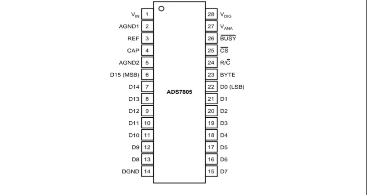
1 VIN Analog Input. See Figure 7.
2 AGND1 Analog Ground. Used internally as ground reference point. 3 REF Reference Input/Output. 2.2µF tantalum capacitor to ground. 4 CAP Reference Buffer Capacitor. 2.2µF tantalum capacitor to ground.
5 AGND2 Analog Ground
6 D15 (MSB) O Data Bit 15. Most Significant Bit (MSB) of conversion results. Hi-Z state when CS is HIGH, or when R/C is LOW. 7 D14 O Data Bit 14. Hi-Z state when CS is HIGH, or when R/C is LOW.
8 D13 O Data Bit 13. Hi-Z state when CS is HIGH, or when R/C is LOW. 9 D12 O Data Bit 12. Hi-Z state when CS is HIGH, or when R/C is LOW. 10 D11 O Data Bit 11. Hi-Z state when CS is HIGH, or when R/C is LOW. 11 D10 O Data Bit 10. Hi-Z state when CS is HIGH, or when R/C is LOW. 12 D9 O Data Bit 9. Hi-Z state when CS is HIGH, or when R/C is LOW. 13 D8 O Data Bit 8. Hi-Z state when CS is HIGH, or when R/C is LOW.
14 DGND Digital Ground
15 D7 O Data Bit 7. Hi-Z state when CS is HIGH, or when R/C is LOW. 16 D6 O Data Bit 6. Hi-Z state when CS is HIGH, or when R/C is LOW. 17 D5 O Data Bit 5. Hi-Z state when CS is HIGH, or when R/C is LOW. 18 D4 O Data Bit 4. Hi-Z state when CS is HIGH, or when R/C is LOW. 19 D3 O Data Bit 3. Hi-Z state when CS is HIGH, or when R/C is LOW. 20 D2 O Data Bit 2. Hi-Z state when CS is HIGH, or when R/C is LOW. 21 D1 O Data Bit 1. Hi-Z state when CS is HIGH, or when R/C is LOW.
22 D0 (LSB) O Data Bit 0. Least Significant Bit (LSB) of conversion results. Hi-Z state when CS is HIGH, or when R/C is LOW. 23 BYTE I Selects 8 most significant bits (LOW) or 8 least significant bits (HIGH).
24 R/C I With CS LOW and BUSY HIGH, a Falling Edge on R/C Initiates a new conversion. With CS LOW, a rising edge on R/C enables the parallel output.
25 CS I Internally OR’d with R/C. If R/C LOW, a falling edge on CS initiates a new conversion.
26 BUSY O At the start of a conversion, BUSY goes LOW and stays LOW until the conversion is completed and the digital outputs have been updated.
27 VANA Analog Supply Input. Nominally +5V. Decouple to ground with 0.1µF ceramic and 10µF tantalum capacitors.
28 VDIG Digital Supply Input. Nominally +5V. Connect directly to pin 27. Must be ≤ VANA.
DIGITAL
PIN # NAME I/O DESCRIPTION
TABLE I. Pin Assignments.
PIN CONFIGURATION
VDIG VANA BUSY CS R/C BYTE D0 (LSB) D1 D2 D3 D4 D5 D6 D7 VIN AGND1 REF CAP AGND2 D15 (MSB) D14 D13 D12 D11 D10 D9 D8 DGND 1 2 3 4 5 6 7 8 9 10 11 12 13 14 28 27 26 25 24 23 22 21 20 19 18 17 16 15 ADS78053 2 1 0 –1 –2 –3 16-Bit LSBs 3 2 1 0 –1 –2 –3 16-Bit LSBs 0 8192 16384 24576 32768 LINEARITY vs CODE Decimal Code 40960 49152 57344 65535 0 8192 16384 24576 32768 Decimal Code 40960 49152 57344 65535 All Codes INL
All Codes DNL
TYPICAL CHARACTERISTICS
TA = +25°C, fS = 100kHz, VDIG = VANA = +5V, using internal reference and fixed resistors shown in Figure 6b, unless otherwise specified.
FREQUENCY SPECTRUM (8192 Point FFT; fIN = 20kHz, 0dB) Frequency (kHz) Amplitude (dB) 0 –20 –40 –60 –80 –100 –120 –140 0.0 12.5 25.0 37.5 50.0 FREQUENCY SPECTRUM (8192 Point FFT; fIN = 45kHz, 0dB) Frequency (kHz) Amplitude (dB) 0 –20 –40 –60 –80 –100 –120 –140 0.0 12.5 25.0 37.5 50.0 50kHz SIGNAL-TO-(NOISE + DISTORTION) vs TEMPERATURE
(fIN = 20kHz, 0dB; fS = 50kHz, 100kHz) 100.0 95.0 90.0 85.0 80.0 75.0 –50 –25 0 25 50 75 100 125 150 Temperature (°C) SINAD (dB) 100kHz SIGNAL-TO-(NOISE + DISTORTION)
vs INPUT FREQUENCY AND INPUT AMPLITUDE 90 80 70 60 50 40 30 20 10 0 SINAD (dB) 0 5 10 15 20 25 30 35 40 45
Input Signal Frequency (kHz) 0dB –20dB –60dB AC PARAMETERS vs TEMPERATURE (fIN = 20kHz, 0dB) 110 105 100 95 90 85 80 –80 –85 –90 –95 –100 –105 –110 SFDR, SNR, and SINAD (dB) THD (dB) –50 –25 0 25 50 75 100 125 150 Temperature (°C) SFDR SNR THD SINAD
TYPICAL CHARACTERISTICS
(Cont.)
TA = +25°C, fS = 100kHz, VDIG = VANA = +5V, using internal reference and fixed resistors shown in Figure 6b, unless otherwise specified.
INTERNAL REFERENCE VOLTAGE vs TEMPERATURE
–50 –25 0 25 50 75 100 125 150 2.520 2.515 2.510 2.505 2.500 2.495 2.490 2.485 2.480 Internal Reference (V) Temperature (°C) Percent From Ideal mV From Ideal Percent From Ideal
BPZ ERROR (INTERNAL REFERENCE)
ENDPOINT ERRORS (EXTERNAL REFERENCE)
ENDPOINT ERRORS (EXTERNAL REFERENCE)
–50 –25 0 25 50 75 Temperature (°C) 8 4 0 –4 –8 0.2 0.1 0.0 –0.1 –0.2 0.2 0.1 0.0 –0.1 –0.2 100 125 150 +FS Error –FS Error
CONVERSION TIME vs TEMPERATURE 8.0 7.9 7.8 7.7 7.6 7.5 7.4 7.3 7.2 –50 150 Temperature (°C) Conversion Time ( µ s) –25 0 25 50 75 100 125
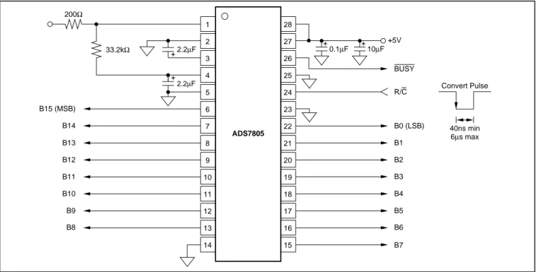
FIGURE 1. Basic Operation.
CS R/C BUSY OPERATION
1 X X None. Databus is in Hi-Z state.
↓ 0 1 Initiates conversion “n”. Databus remains in Hi-Z state.
0 ↓ 1 Initiates conversion “n”. Databus enters Hi-Z state.
0 1 ↑ Conversion “n” completed. Valid data from conversion “n” on the databus.
↓ 1 1 Enables databus with valid data from conversion “n”.
↓ 1 0 Enables databus with valid data from conversion “n-1”(1). Conversion n in progress.
0 ↑ 0 Enables databus with valid data from conversion “n-1”(1). Conversion “n” in progress.
0 0 ↑ New conversion initiated without acquisition of a new signal. Data will be invalid. CS and/or R/C must be HIGH when BUSY goes HIGH.
X X 0 New convert commands ignored. Conversion
“n” in progress.
NOTE: (1) See Figures 3 and 4 for constraints on data valid from conversion “n-1”.
Table II. Control Line Functions for “Read” and “Convert”.
1 2 3 4 5 6 7 8 9 10 11 12 13 14 28 27 26 25 24 23 22 21 20 19 18 17 16 15 ADS7805 200Ω 33.2kΩ +5V 0.1µF 10µF + + 2.2µF + + 2.2µF Convert Pulse 40ns min 6µs max B4 B5 B6 B7 B2 B1 B0 (LSB) R/C BUSY B3 B10 B9 B8 B11 B12 B13 B14 B15 (MSB)
BASIC OPERATION
Figure 1 shows a basic circuit to operate the ADS7805 with a full parallel data output. Taking R/C (pin 24) LOW for a minimum of 40ns (7µs max) will initiate a conversion. BUSY (pin 26) will go LOW and stay LOW until the conversion is completed and the output registers are updated. Data will be output in Binary Two’s Complement with the MSB on pin 6. BUSY going HIGH can be used to latch the data. All convert commands will be ignored while BUSY is LOW.
The ADS7805 will begin tracking the input signal at the end of the conversion. Allowing 10µs between convert com-mands assures accurate acquisition of a new signal. The offset and gain are adjusted internally to allow external trimming with a single supply. The external resistors com-pensate for this adjustment and can be left out if the offset and gain will be corrected in software (refer to the “Calibra-tion” section).
STARTING A CONVERSION
The combination of CS (pin 25) and R/C (pin 24) LOW for a minimum of 40ns immediately puts the sample-and-hold of the ADS7805 in the hold state and starts conversion ‘n’. BUSY (pin 26) will go LOW and stay LOW until conversion ‘n’ is completed and the internal output register has been updated. All new convert commands during BUSY LOW will be ignored. CS and/or R/C must go HIGH before BUSY goes HIGH or a new conversion will be initiated without sufficient time to acquire a new signal.
The ADS7805 will begin tracking the input signal at the end of the conversion. Allowing 10µs between convert com-mands assures accurate acquisition of a new signal. Refer to
Table II for a summary of CS, R/C, and BUSY states and Figures 3 through 5 for timing diagrams.
CS and R/C are internally OR’d and level triggered. There is not a requirement which input goes LOW first when initiating a conversion. If, however, it is critical that CS or R/C initiates conversion ‘n’, be sure the less critical input is LOW at least 10ns prior to the initiating input.
To reduce the number of control pins, CS can be tied LOW using R/C to control the read and convert modes. This will have no effect when using the internal data clock in the serial output mode. However, the parallel output will become active whenever R/C goes HIGH. Refer to the “Reading Data” section.
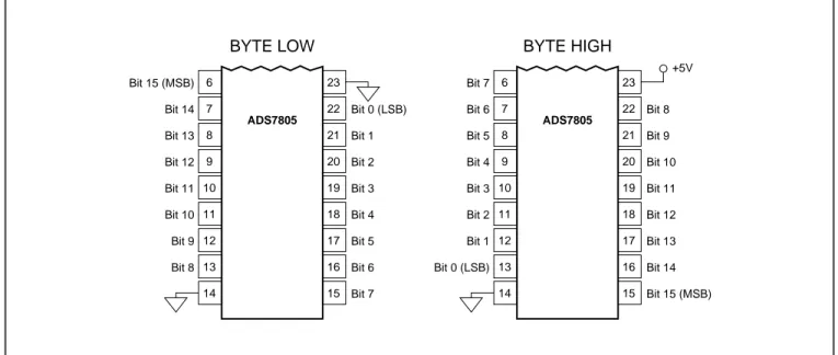
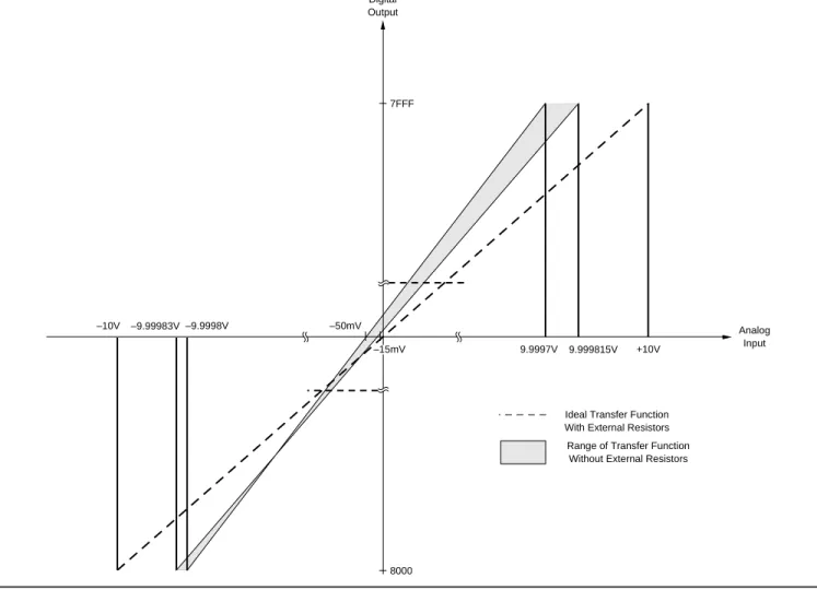
FIGURE 2. Bit Locations Relative to State of BYTE (pin 23). DIGITAL OUTPUT BINARY TWO’S COMPLEMENT DESCRIPTION ANALOG INPUT BINARY CODE HEX CODE Full-Scale Range ±10V Least Significant 305µV Bit (LSB) +Full Scale 9.999695V 0111 1111 1111 1111 7FFF (10V – 1LSB) Mid-scale 0V 0000 0000 0000 0000 0000 One LSB below –305µV 1111 1111 1111 1111 FFFF Mid-scale –Full Scale –10V 1000 0000 0000 0000 8000
Table III. Ideal Input Voltages and Output Codes.
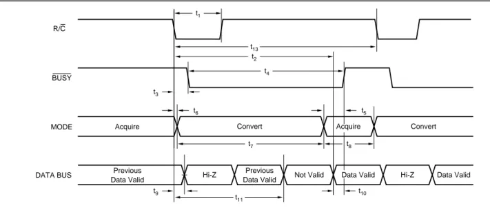
SYMBOL DESCRIPTION MIN TYP MAX UNITS
t1 Convert Pulse Width 40 7000 ns
t2 Data Valid Delay after R/C LOW 8 µs
t3 BUSY Delay from R/C LOW 65 ns
t4 BUSY LOW 8 µs
t5 BUSY Delay after 220 ns
End of Conversion
t6 Aperture Delay 40 ns
t7 Conversion Time 7.6 8 µs
t8 Acquisition Time 2 µs
t9 Bus Relinquish Time 10 35 83 ns
t10 BUSY Delay after Data Valid 50 200 ns
t11 Previous Data Valid 7.4 µs
after R/C LOW
t7 + t6 Throughput Time 9 10 µs
t12 R/C to CS Setup Time 10 ns
t13 Time Between Conversions 10 µs
t14 Bus Access Time 10 83 ns
and BYTE Delay TABLE IV. Conversion Timing.
Bit 0 (LSB) Bit 1 Bit 2 Bit 3 Bit 4 Bit 5 Bit 6 Bit 7 Bit 15 (MSB) Bit 14 Bit 13 Bit 12 Bit 11 Bit 10 Bit 9 Bit 8 6 7 8 9 10 11 12 13 14 23 22 21 20 19 18 17 16 15 ADS7805
BYTE LOW
Bit 8 Bit 9 Bit 10 Bit 11 Bit 12 Bit 13 Bit 14 Bit 15 (MSB) Bit 7 Bit 6 Bit 5 Bit 4 Bit 3 Bit 2 Bit 1 Bit 0 (LSB) 6 7 8 9 10 11 12 13 14 23 22 21 20 19 18 17 16 15 ADS7805BYTE HIGH
+5VREADING DATA
The ADS7805 outputs full or byte-reading parallel data in Binary Two’s Complement data output format. The parallel output will be active when R/C (pin 24) is HIGH and CS (pin 25) is LOW. Any other combination of CS and R/C will tri-state the parallel output. Valid conversion data can be read in a full parallel, 16-bit word or two 8-bit bytes on pins 6-13 and pins 15-22. BYTE (pin 23) can be toggled to read both bytes within one conversion cycle. Refer to Table III for ideal output codes and Figure 2 for bit locations relative to the state of BYTE.
PARALLEL OUTPUT (After a Conversion)
After conversion ‘n’ is completed and the output registers have been updated, BUSY (pin 26) will go HIGH. Valid data from conversion ‘n’ will be available on D15-D0 (pins 6-13 and 15-22). BUSY going HIGH can be used to latch the data. Refer to Table IV and Figures 3 to 5 for timing specifications.
PARALLEL OUTPUT (During a Conversion)
After conversion ‘n’ has been initiated, valid data from con-version ‘n – 1’ can be read and will be valid up to 7µs after the start of conversion ‘n’. Do not attempt to read data from 7µs after the start of conversion ‘n’ until BUSY (pin 26) goes HIGH; this may result in reading invalid data. Refer to Table IV and Figures 3 to 5 for timing specifications.Note! For the best possible performance, data should not be
read during a conversion. The switching noise of the asyn-chronous data transfer can cause digital feedthrough de-grading the converter’s performance.
The number of control lines can be reduced by tying CS LOW while using R/C to initiate conversions and activate the output mode of the converter (see Figure 3).
FIGURE 5. Using CS and BYTE to Control Data Bus.
t8 BUSY
R/C
MODE Acquire Convert Convert
t7 t6 t3 t4 t1 t2 t5
DATA BUS Previous
Data Valid
t10
Hi-Z Data Valid Hi-Z Previous
Data Valid Not Valid t11
t9
Acquire
Data Valid t13
FIGURE 3. Conversion Timing with Outputs Enabled after Conversion (CS Tied LOW).
FIGURE 4. Using CS to Control Conversion and Read Timing.
t12 t12
t14 Hi-Z High Byte
t14
Low Byte Hi-Z t9
Hi-Z Low Byte High Byte Hi-Z
Pins 6-13 Pins 15-22 BYTE CS R/C t9 Hi-Z State BUSY R/C DATA BUS MODE Acquire
Data Valid Hi-Z State Convert t7 t6 t3 t4 t12 Acquire t14 t12 t1 t12 t12 CS
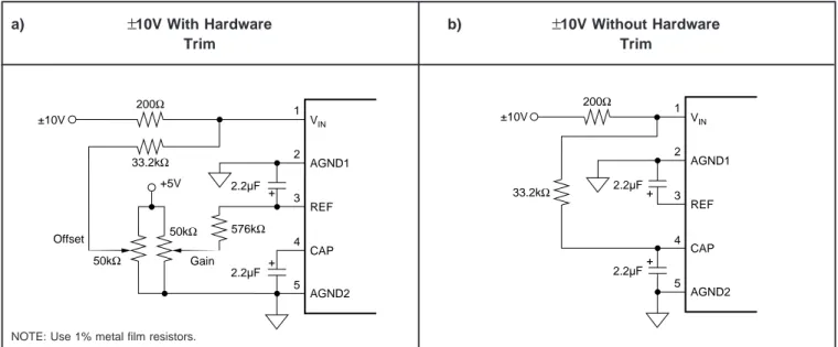
FIGURE 6. Circuit Diagram With and Without External Resistors.
a)
±
10V With Hardware Trimb)
±
10V Without Hardware TrimNOTE: Use 1% metal film resistors.
WITH WITHOUT
EXTERNAL EXTERNAL
RESISTORS RESISTORS UNITS
BP0 –10 < BPO < 10 –50 < BPO < –15 mV –30 < BPO < 30 –150 < BPO < –45 LSBs Gain –0.5 < error < 0.5 –2 < error < –1 % of FSR Error
TABLE V. Offset and Gain Errors With and Without External Resistors. 200Ω 1 2 3 4 5 AGND2 CAP REF AGND1 VIN + 2.2µF +5V 50kΩ 50kΩ 33.2kΩ 576kΩ + 2.2µF Gain ±10V Offset 200Ω 1 2 3 4 5 AGND2 CAP REF AGND1 VIN + 2.2µF 33.2kΩ ±10V + 2.2µF
INPUT RANGES
The ADS7805 offers a standard ±10V input range. Figure 6 shows the necessary circuit connections for the ADS7805 with and without hardware trim. Offset and full-scale error(1)
specifications are tested and specified with the fixed resistors shown in Figure 6b. Adjustments for offset and gain are described in the “Calibration” section of this data sheet. The offset and gain are adjusted internally to allow external trimming with a single supply. The external resistors com-pensate for this adjustment and can be left out if the offset and gain will be corrected in software (refer to the “Calibra-tion” section).
The nominal input impedance of 23kΩ results from the combi-nation of the internal resistor network shown on the front page of the product data sheet and the external resistors. The input resistor divider network provides inherent overvoltage protec-tion ensured to at least ±25V. The 1% resistors used for the external circuitry do not compromise the accuracy or drift of the converter. They have little influence relative to the internal resistors, and tighter tolerances are not required.
NOTE: (1) Full-scale error includes offset and gain errors measured at both +FS and –FS.
CALIBRATION
The ADS7805 can be trimmed in hardware or software. The offset should be trimmed before the gain since the offset directly affects the gain. To achieve optimum performance, several iterations may be required.
HARDWARE CALIBRATION
To calibrate the offset and gain of the ADS7805, install the proper resistors and potentiometers as shown in Figure 6a. The calibration range is ±15mV for the offset and ±60mV for the gain.
SOFTWARE CALIBRATION
To calibrate the offset and gain of the ADS7805 in software, no external resistors are required. See the “No Calibration” sec-tion for details on the effects of the external resistors. Range of offset and gain errors with and without external resistors is shown in Table V.
NO CALIBRATION
Figure 6b shows circuit connections. The external resistors shown in Figure 6b may not be necessary in some applica-tions. These resistors provide compensation for an internal adjustment of the offset and gain which allows calibration with a single supply. The nominal transfer function of the ADS7805 will be bound by the shaded region (see Figure 7) with a typical offset of –30mV and a typical gain error of –1.5%. Refer to Table V for range of offset and gain errors with and without external resistors.
FIGURE 7. Full-Scale Transfer Function. –9.99983V –9.9998V –10V Digital Output 7FFF Analog Input 8000 9.999815V +10V
Ideal Transfer Function With External Resistors
Range of Transfer Function Without External Resistors 9.9997V
–50mV
–15mV
REFERENCE
The ADS7805 can operate with its internal 2.5V reference or an external reference. By applying an external reference to pin 5, the internal reference can be bypassed. The reference voltage at REF is buffered internally with the output on CAP (pin 4).
The internal reference has an 8 ppm/°C drift (typical) and accounts for approximately 20% of the full-scale error (FSE = ±0.5% for low grade, ±0.25% for high grade).
REF
REF (pin 3) is an input for an external reference or the output for the internal 2.5V reference. A 2.2µF capacitor should be connected as close to the REF pin as possible. The capacitor and the output resistance of REF create a low-pass filter to bandlimit noise on the reference. Using a smaller value capacitor will introduce more noise to the reference degrad-ing the SNR and SINAD. The REF pin should not be used to drive external AC or DC loads.
The range for the external reference is 2.3V to 2.7V and determines the actual LSB size. Increasing the reference voltage will increase the full-scale range and the LSB size of the converter which can improve the SNR.
CAP
CAP (pin 4) is the output of the internal reference buffer. A 2.2µF capacitor should be placed as close to the CAP pin as possible to provide optimum switching currents for the CDAC throughout the conversion cycle and compensation for the output of the internal buffer. Using a capacitor any smaller than 1µF can cause the output buffer to oscillate and may not have sufficient charge for the CDAC. Capacitor values larger than 2.2µF will have little effect on improving performance. The output of the buffer is capable of driving up to 2mA of current to a DC load. DC loads requiring more than 2mA of current from the CAP pin will begin to degrade the linearity of the ADS7805. Using an external buffer will allow the internal reference to be used for larger DC loads and AC loads. Do not attempt to directly drive an AC load with the output voltage on CAP. This will cause performance degra-dation of the converter.
LAYOUT
POWER
For optimum performance, tie the analog and digital power pins to the same +5V power supply and tie the analog and digital grounds together. As noted in the electrical specifica-tions, the ADS7805 uses 90% of its power for the analog circuitry. The ADS7805 should be considered as an analog component.
The +5V power for the A/D converter should be separate from the +5V used for the system’s digital logic. Connecting VDIG (pin 28) directly to a digital supply can reduce converter performance due to switching noise from the digital logic. For best performance, the +5V supply can be produced from whatever analog supply is used for the rest of the analog signal conditioning. If +12V or +15V supplies are present, a simple +5V regulator can be used. Although it is not sug-gested, if the digital supply must be used to power the converter, be sure to properly filter the supply. Either using a filtered digital supply or a regulated analog supply, both VDIG and VANA should be tied to the same +5V source.
GROUNDING
Three ground pins are present on the ADS7805. DGND is the digital supply ground. AGND2 is the analog supply ground. AGND1 is the ground which all analog signals internal to the A/D converter are referenced. AGND1 is more susceptible to current induced voltage drops and must have the path of least resistance back to the power supply. All the ground pins of the A/D converter should be tied to the analog ground plane, separated from the system’s digital logic ground, to achieve optimum performance. Both analog and digital ground planes should be tied to the “system” ground as near to the power supplies as possible. This helps to prevent dynamic digital ground currents from modulating the analog ground through a common impedance to power ground.
SIGNAL CONDITIONING
The FET switches used for the sample-and-hold on many CMOS A/D converters release a significant amount of charge injection which can cause the driving op amp to oscillate. The FET switch on the ADS7805, compared to the FET switches on other CMOS A/D converters, releases 5%-10% of the charge. There is also a resistive front end which attenuates any charge which is released. The end result is a minimal requirement for the anti-alias filter on the front end. Any op amp sufficient for the signal in an application will be sufficient to drive the ADS7805.
The resistive front end of the ADS7805 also provides an ensured ±25V overvoltage protection. In most cases, this eliminates the need for external input protection circuitry.
INTERMEDIATE LATCHES
The ADS7805 does have tri-state outputs for the parallel port, but intermediate latches should be used if the bus will be active during conversions. If the bus is not active during conversion, the tri-state outputs can be used to isolate the A/D converter from other peripherals on the same bus. Tri-state outputs can also be used when the A/D converter is the only peripheral on the data bus.
Intermediate latches are beneficial on any monolithic A/D converter. The ADS7805 has an internal LSB size of 38µV. Transients from fast switching signals on the parallel port, even when the A/D converter is tri-stated, can be coupled through the substrate to the analog circuitry causing degra-dation of converter performance.
DATE REVISION PAGE SECTION DESCRIPTION
3 Absolute Maximum Ratings CAP and REF were switched. 2 Package/Ordering Information Corrected typos in ordering table.
Revision History
NOTE: Page numbers for previous revisions may differ from page numbers in the current version.
10/06 D
PACKAGE OPTION ADDENDUM
www.ti.com 15-Oct-2015
PACKAGING INFORMATION
Orderable Device Status
(1)
Package Type Package Drawing Pins Package Qty Eco Plan (2) Lead/Ball Finish (6) MSL Peak Temp (3)
Op Temp (°C) Device Marking
(4/5)
Samples
ADS7805U NRND SOIC DW 28 20 Green (RoHS
& no Sb/Br)
CU NIPDAU-DCC Level-3-260C-168 HR ADS7805U
B
ADS7805U/1K NRND SOIC DW 28 1000 Green (RoHS
& no Sb/Br)
CU NIPDAU-DCC Level-3-260C-168 HR ADS7805U
B
ADS7805U/1KE4 NRND SOIC DW 28 1000 Green (RoHS
& no Sb/Br)
CU NIPDAU-DCC Level-3-260C-168 HR -25 to 85 ADS7805U B
ADS7805UB NRND SOIC DW 28 20 Green (RoHS
& no Sb/Br)
CU NIPDAU-DCC Level-3-260C-168 HR ADS7805U
B
ADS7805UB/1K NRND SOIC DW 28 1000 Green (RoHS
& no Sb/Br)
CU NIPDAU-DCC Level-3-260C-168 HR ADS7805U
B
ADS7805UBE4 NRND SOIC DW 28 20 Green (RoHS
& no Sb/Br)
CU NIPDAU-DCC Level-3-260C-168 HR -25 to 85 ADS7805U B
ADS7805UBG4 NRND SOIC DW 28 20 Green (RoHS
& no Sb/Br)
CU NIPDAU-DCC Level-3-260C-168 HR ADS7805U
B
ADS7805UE4 NRND SOIC DW 28 20 Green (RoHS
& no Sb/Br)
CU NIPDAU-DCC Level-3-260C-168 HR -25 to 85 ADS7805U B
ADS7805UG4 NRND SOIC DW 28 20 Green (RoHS
& no Sb/Br)
CU NIPDAU-DCC Level-3-260C-168 HR ADS7805U
B (1)
The marketing status values are defined as follows:
ACTIVE: Product device recommended for new designs.
LIFEBUY: TI has announced that the device will be discontinued, and a lifetime-buy period is in effect.
NRND: Not recommended for new designs. Device is in production to support existing customers, but TI does not recommend using this part in a new design. PREVIEW: Device has been announced but is not in production. Samples may or may not be available.
OBSOLETE: TI has discontinued the production of the device.
(2)
Eco Plan - The planned eco-friendly classification: Pb-Free (RoHS), Pb-Free (RoHS Exempt), or Green (RoHS & no Sb/Br) - please check http://www.ti.com/productcontent for the latest availability information and additional product content details.
TBD: The Pb-Free/Green conversion plan has not been defined.
Pb-Free (RoHS): TI's terms "Lead-Free" or "Pb-Free" mean semiconductor products that are compatible with the current RoHS requirements for all 6 substances, including the requirement that
lead not exceed 0.1% by weight in homogeneous materials. Where designed to be soldered at high temperatures, TI Pb-Free products are suitable for use in specified lead-free processes.
Pb-Free (RoHS Exempt): This component has a RoHS exemption for either 1) lead-based flip-chip solder bumps used between the die and package, or 2) lead-based die adhesive used between
the die and leadframe. The component is otherwise considered Pb-Free (RoHS compatible) as defined above.
Green (RoHS & no Sb/Br): TI defines "Green" to mean Pb-Free (RoHS compatible), and free of Bromine (Br) and Antimony (Sb) based flame retardants (Br or Sb do not exceed 0.1% by weight
PACKAGE OPTION ADDENDUM
www.ti.com 15-Oct-2015
(3)
MSL, Peak Temp. - The Moisture Sensitivity Level rating according to the JEDEC industry standard classifications, and peak solder temperature. (4)
There may be additional marking, which relates to the logo, the lot trace code information, or the environmental category on the device. (5)
Multiple Device Markings will be inside parentheses. Only one Device Marking contained in parentheses and separated by a "~" will appear on a device. If a line is indented then it is a continuation of the previous line and the two combined represent the entire Device Marking for that device.
(6)
Lead/Ball Finish - Orderable Devices may have multiple material finish options. Finish options are separated by a vertical ruled line. Lead/Ball Finish values may wrap to two lines if the finish value exceeds the maximum column width.
Important Information and Disclaimer:The information provided on this page represents TI's knowledge and belief as of the date that it is provided. TI bases its knowledge and belief on information
provided by third parties, and makes no representation or warranty as to the accuracy of such information. Efforts are underway to better integrate information from third parties. TI has taken and continues to take reasonable steps to provide representative and accurate information but may not have conducted destructive testing or chemical analysis on incoming materials and chemicals. TI and TI suppliers consider certain information to be proprietary, and thus CAS numbers and other limited information may not be available for release.
TAPE AND REEL INFORMATION
*All dimensions are nominal
Device Package Type Package Drawing Pins SPQ Reel Diameter (mm) Reel Width W1 (mm) A0 (mm) B0 (mm) K0 (mm) P1 (mm) W (mm) Pin1 Quadrant ADS7805U/1K SOIC DW 28 1000 330.0 32.4 11.35 18.67 3.1 16.0 32.0 Q1 ADS7805UB/1K SOIC DW 28 1000 330.0 32.4 11.35 18.67 3.1 16.0 32.0 Q1
PACKAGE MATERIALS INFORMATION
*All dimensions are nominal
Device Package Type Package Drawing Pins SPQ Length (mm) Width (mm) Height (mm)
ADS7805U/1K SOIC DW 28 1000 367.0 367.0 55.0
ADS7805UB/1K SOIC DW 28 1000 367.0 367.0 55.0
PACKAGE MATERIALS INFORMATION
www.ti.com 14-Jul-2015
IMPORTANT NOTICE
Texas Instruments Incorporated and its subsidiaries (TI) reserve the right to make corrections, enhancements, improvements and other changes to its semiconductor products and services per JESD46, latest issue, and to discontinue any product or service per JESD48, latest issue. Buyers should obtain the latest relevant information before placing orders and should verify that such information is current and complete. All semiconductor products (also referred to herein as “components”) are sold subject to TI’s terms and conditions of sale supplied at the time of order acknowledgment.
TI warrants performance of its components to the specifications applicable at the time of sale, in accordance with the warranty in TI’s terms and conditions of sale of semiconductor products. Testing and other quality control techniques are used to the extent TI deems necessary to support this warranty. Except where mandated by applicable law, testing of all parameters of each component is not necessarily performed.
TI assumes no liability for applications assistance or the design of Buyers’ products. Buyers are responsible for their products and applications using TI components. To minimize the risks associated with Buyers’ products and applications, Buyers should provide adequate design and operating safeguards.
TI does not warrant or represent that any license, either express or implied, is granted under any patent right, copyright, mask work right, or other intellectual property right relating to any combination, machine, or process in which TI components or services are used. Information published by TI regarding third-party products or services does not constitute a license to use such products or services or a warranty or endorsement thereof. Use of such information may require a license from a third party under the patents or other intellectual property of the third party, or a license from TI under the patents or other intellectual property of TI.
Reproduction of significant portions of TI information in TI data books or data sheets is permissible only if reproduction is without alteration and is accompanied by all associated warranties, conditions, limitations, and notices. TI is not responsible or liable for such altered documentation. Information of third parties may be subject to additional restrictions.
Resale of TI components or services with statements different from or beyond the parameters stated by TI for that component or service voids all express and any implied warranties for the associated TI component or service and is an unfair and deceptive business practice. TI is not responsible or liable for any such statements.
Buyer acknowledges and agrees that it is solely responsible for compliance with all legal, regulatory and safety-related requirements concerning its products, and any use of TI components in its applications, notwithstanding any applications-related information or support that may be provided by TI. Buyer represents and agrees that it has all the necessary expertise to create and implement safeguards which anticipate dangerous consequences of failures, monitor failures and their consequences, lessen the likelihood of failures that might cause harm and take appropriate remedial actions. Buyer will fully indemnify TI and its representatives against any damages arising out of the use of any TI components in safety-critical applications.
In some cases, TI components may be promoted specifically to facilitate safety-related applications. With such components, TI’s goal is to help enable customers to design and create their own end-product solutions that meet applicable functional safety standards and requirements. Nonetheless, such components are subject to these terms.
No TI components are authorized for use in FDA Class III (or similar life-critical medical equipment) unless authorized officers of the parties have executed a special agreement specifically governing such use.
Only those TI components which TI has specifically designated as military grade or “enhanced plastic” are designed and intended for use in military/aerospace applications or environments. Buyer acknowledges and agrees that any military or aerospace use of TI components which havenotbeen so designated is solely at the Buyer's risk, and that Buyer is solely responsible for compliance with all legal and regulatory requirements in connection with such use.
TI has specifically designated certain components as meeting ISO/TS16949 requirements, mainly for automotive use. In any case of use of non-designated products, TI will not be responsible for any failure to meet ISO/TS16949.
Products Applications
Audio www.ti.com/audio Automotive and Transportation www.ti.com/automotive
Amplifiers amplifier.ti.com Communications and Telecom www.ti.com/communications
Data Converters dataconverter.ti.com Computers and Peripherals www.ti.com/computers
DLP® Products www.dlp.com Consumer Electronics www.ti.com/consumer-apps
DSP dsp.ti.com Energy and Lighting www.ti.com/energy
Clocks and Timers www.ti.com/clocks Industrial www.ti.com/industrial
Interface interface.ti.com Medical www.ti.com/medical
Logic logic.ti.com Security www.ti.com/security
Power Mgmt power.ti.com Space, Avionics and Defense www.ti.com/space-avionics-defense
Microcontrollers microcontroller.ti.com Video and Imaging www.ti.com/video
RFID www.ti-rfid.com
OMAP Applications Processors www.ti.com/omap TI E2E Community e2e.ti.com
Wireless Connectivity www.ti.com/wirelessconnectivity
Mailing Address: Texas Instruments, Post Office Box 655303, Dallas, Texas 75265 Copyright © 2015, Texas Instruments Incorporated