Optical Characterization of Organic
Semiconducting Single Crystals
by
Jennifer Weinberg-Wolf
A dissertation submitted to the faculty of the University of North Carolina at Chapel Hill in partial fulfillment of the requirements for the degree of Doctor of Philosophy in the Department of Physics & Astronomy.
Chapel Hill
2006
Approved by:
c °2006
Jennifer Weinberg-Wolf
ABSTRACT
Jennifer Weinberg-Wolf: Optical Characterization of Organic Semiconducting Single Crystals
(Under the Direction of Dr. Laurie McNeil)
Over the last decade interest in the possibility of “plastic electronics,”
semi-conducting organic materials that hold the potential for display devices with
improved characteristics, has increased. To date, the majority of research has
fo-cused on material development and device design. However, if scientists are able
to understand the connection between the structural and electronic properties
of molecules, they can tailor new compounds with desired physical
characteris-tics. Optical characterization is the first step to understanding the structural
properties of materials.
This work focuses on characterizing single crystals of two specific molecules:
α-hexathiophene and 5,6,11,12-tetraphenyl tetracene (rubrene). While there is
plenty of information currently available in the literature aboutα-hexathiophene,
the resonant Raman experiments I describe in Chapter 3 have uncovered the
low-est experimentally-recorded excited electronic levels. I have tentatively identified
these states as either a triplet Frenkel exciton or a bound singlet Frenkel exciton.
Chapter 4 details how I used Raman, infrared and photoluminescence
spec-troscopy, as well as computer simulations, to characterize rubrene. Studies of
tetracene single crystals helped guide the understanding of the structural and
electronic properties of rubrene. Although all molecular crystals have low
in-termolecular coupling, my analysis showed that rubrene has particularly low
coupling, even for a molecular crystal. This result goes against commonly held
belief that the best molecules for “plastic electronic” devices should have strong
clearly reveals emission from free carriers as well as free charge transfer excitons,
ACKNOWLEDGMENTS
There are many people who helped make this document and the research
behind it possible. First, I have to thank my advisor, Laurie McNeil, without
whose guidance, support, and equipment this project would not have been
pos-sible. She has been a wonderful mentor, knowing when to give much needed
direction and when to let me work out problems on my own. I would also like to
thank the other members of my committee, John Hernandez, John Papanikolas,
Richard Superfine, Ed Samulski and Otto Zhou for their time, attention, and
helpful suggestions and comments throughout this entire project.
Incredibly important collaborators who I must mention, praise and thank are
Christian Kloc at Lucent Technologies, who supplied all of my materials; and
Shubin Liu of the High Performance Computing Group at UNC, who ran the
dif-ferent theoretical calculations. Although not directly working on the same
scien-tific questions, my class-mates and lab-mates over the last seven years have been a
crucial component of my success. They served as sounding boards for discussion,
extra sets of hands for countless alignment procedures, great sources of
informa-tion, good company and all around good friends. Thank you to Jim Crooks, Kris
Capella, Jessica Owens, Chris Lawyer, Russell Walker, Kris McGuire, Zhongqiao
Ren and especially Eric Harley.
There is no question in my mind that I would not have achieved what I have
today without the support of many individuals: friends, teachers and family
throughout my life. I am fortunate enough to have too many people to thank
individually, but special recognition must be given to some outstanding
my in-laws who always ask what I am currently working on, fantastic physics
teachers who inspired me to continue studying a subject I have learned to love
and my sisters for bragging about their big sister, the physicist. My parents,
Margot and Alan, always encouraged me to take the hardest science classes I
could and not be discouraged by obstacles. They taught me it was ok to be
different, to love to learn and to be excited rather than intimidated when I was
the only girl in the classroom. I would not have accomplished this work without
their support.
Last, but definitely not least, I must thank my wonderful husband, Jonathan
Miller, who put up with me for so many years through the entire graduate school
process. Without him I would have spent many lonely, hungry nights in lab.
Instead he would keep me company through seemingly endless numbers of scans
and bring picnic meals to lab when I couldn’t leave. He also served as my personal
system administrator, making sure my computers worked, debugging my code
and helping me to implement (sometimes just actually writing) data analysis and
molecular visualization scripts. But most important was his unwavering support
and love for which I cannot thank him enough.
Jennifer Weinberg-Wolf
CONTENTS
Page
LIST OF TABLES . . . . x
LIST OF FIGURES . . . . xi
Chapter I. Introduction . . . . 1
1.1 Overview . . . . 1
1.2 Molecular Crystals . . . . 3
1.2.1 Oligothiophenes: Alpha-hexathiophene . . . . 4
1.2.2 Oligoacenes: Tetracene and Rubrene . . . . 7
II. Experimental Techniques . . . . 12
2.1 Crystal Growth . . . . 12
2.2 Raman Spectroscopy . . . . 13
2.2.1 Classical Theory . . . . 14
2.2.2 Quantum Theory . . . . 16
2.2.3 Temperature Effects . . . . 19
2.2.4 Resonant Raman Effect . . . . 20
2.2.5 Experimental Setup . . . . 21
2.3 Infrared Spectroscopy . . . . 23
2.4 Photoluminescence Spectroscopy . . . . 24
2.4.1 Photoluminescence Theory . . . . 25
2.4.2 Temperature Effects . . . . 30
2.4.3 Experimental Setup . . . . 30
III. Raman Spectroscopy of Alpha-Hexathiophene . . . . 33
3.1 Alpha-Hexathiophene Crystals . . . . 33
3.2 Room Temperature Experiments. . . . 37
3.3 Temperature Dependent Raman . . . . 42
3.4 Resonant Raman Spectroscopy . . . . 44
3.4.1 Results . . . . 47
3.4.2 Frenkel Excitons . . . . 49
3.4.3 Temperature Dependence of Resonances . . . . 51
3.5 Conclusion . . . . 54
IV. Optical Characterization of Rubrene and Tetracene . . . . 55
4.1 Raman Measurements . . . . 55
4.1.1 Rubrene and Tetracene Crystals . . . . 55
4.1.2 Experimental Conditions . . . . 58
4.1.3 Computer Simulations . . . . 60
4.1.4 Rubrene Single Crystal Raman Results . . . . 60
4.1.5 Comparison to Theory . . . . 62
4.1.6 Tetracene Single Crystal Spectrum . . . . 68
4.1.7 Comparison of Rubrene and Tetracene Spectra . . . . . 72
4.1.8 Temperature Dependence of Rubrene Spectra . . . . . 75
4.1.9 Intermolecular Coupling in Rubrene Single Crystals . . 76
4.2 Infrared Spectrum of Rubrene . . . . 80
4.3 Photoluminescence of Rubrene . . . . 86
4.3.1 Crystals and Experimental Setup . . . . 86
4.3.2 Low Temperature Photoluminescence Results . . . . . 86
4.3.3 Comparison to Theory . . . . 89
4.3.4 Temperature Dependence of Rubrene PL Spectra . . . 91
4.3.5 Rubrene PL Dependence on Photoexcitation Energy. . 95
4.4 Conclusion . . . . 98
LIST OF TABLES
3.1 Comparison of Experimental and Theoretical Structure of α
-hexathiophene. . . . 34
3.2 Experimentally-Measured and Theoretically-Predicted Intramolec-ular Raman Modes for α-hexathiophene . . . . 39
3.3 Highlights From Table 3.2 . . . . 43
3.4 Additional Intramolecular Raman Modes . . . . 47
3.5 Intermolecular Resonant Raman Modes of α-hexathiophene . . . . . 47
4.1 Atomic Positions in Rubrene and Tetracene . . . . 57
4.2 Allowed Raman Modes for Backscattering Geometry . . . . 62
4.3 Irreducible Representation for the Isolated Rubrene Molecule . . . . . 66
4.4 Character Table for the C2h Point Group . . . . 66
4.5 Peak Positions for Measured and Calculated Raman Spectra of Rubrene . . . . 67
4.6 Frequency of Experimental and Theoretical Intramolecular Modes for Tetracene . . . . 72
4.7 Temperature Dependence of Rubrene Intramolecular Modes . . . . . 75
4.8 Densities and Mobilities of Oligoacenes . . . . 79
4.9 Predicted and Measured Infrared Peak Positions and Intensities . . . 81
LIST OF FIGURES
1.1 Oligothiophene Molecules . . . . 4
1.2 Oligoacene Molecules . . . . 7
1.3 Diagram of a Rubrene Molecule . . . . 9
2.1 Light Scattering Schematic . . . . 13
2.2 Feynman Diagrams for Stokes Scattering . . . . 16
2.3 Raman Spectrometer Schematic . . . . 21
2.4 Photoluminescence Schematic . . . . 25
2.5 Photoluminescence Spectrometer Schematic . . . . 32
3.1 Alpha-hexathiophene (C20H14S6) Molecule . . . . 34
3.2 Molecular Stacking in α-hexathiophene Unit Cell . . . . 35
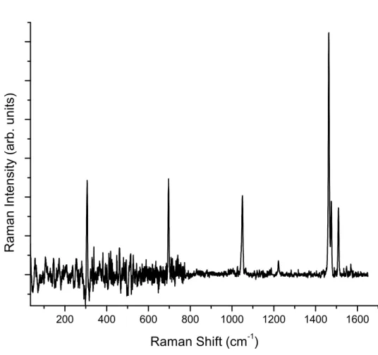
3.3 Room Temperature Raman Spectrum of α-hexathiophene. . . . 38
3.4 Changes in the α-hexathiophene Spectra with Temperature. . . . 44
3.5 Temperature Dependence of Raman Modes of α-hexathiophene . . . 45
3.6 On and Off Resonance Raman Spectra of α-hexathiophene . . . . 46
3.7 Resonance Profiles for α-hexathiophene . . . . 48
3.8 Temperature Dependence of the Resonance Profile of α-hexathiophene 52 4.1 Rubrene (C42H28) Molecule. . . . . 56
4.2 Three Views of the Packing in the Rubrene Single Crystals . . . . 58
4.3 Tetracene (C18H12) Molecule . . . . 59
4.4 Room Temperature Raman Spectrum of Rubrene Single Crystals . . 63
4.5 Experimental vs. Theoretical Peak Positions for Rubrene Sin-gle Crystals . . . . 64
4.6 Experimental vs. Theoretical Peak Positions for Tetracene Single Crystals . . . . 69
4.7 Room Temperature Raman Spectrum of Tetracene Single Crystals . . 70
4.9 Temperature Dependence of Low-frequency Raman Modes of
Rubrene Single Crystals . . . . 76
4.10 Infrared Theoretical and Experimental Spectrum for Rubrene
Single Crystals . . . . 82
4.11 Experimental vs. Theoretical Peak Positions for Infrared
Spectrum of Rubrene Single Crystals . . . . 83
4.12 One Low Temperature Photoluminescence Spectrum of Rubrene
Single Crystals . . . . 87
4.13 Low Temperature Photoluminescence Spectra of Rubrene
Sin-gle Crystals from Multiple Crystallites . . . . 88
4.14 Example Fit of PL Spectrum of Rubrene at 18 K . . . . 90
4.15 Temperature Dependence of Rubrene PL Spectra . . . . 92
4.16 PL Spectra of Rubrene Single Crystals with 496.5 nm
Exci-tation Source . . . . 96
4.17 PL Spectra of Rubrene Single Crystals with Multiple Incident
Chapter 1
Introduction
1.1
Overview
Within the last 50 years, interest has grown in the optical properties of organic
molecular crystals. Many books and reviews of interesting optically-active
mate-rials are available in the literature [1,2]. When researchers first successfully
fabri-cated an all-organic light-emitting device (OLED) using tris-8-hydroxyquinoline
aluminum (Alq3) in 1987 [3], interest in the applications of thin films of these
optically-active organic molecular materials grew. Thus began the development
of a new commercial product: all-organic displays based on OLEDs and
or-ganic field-effect transistors (OFETs). Horowitz recently published a good
re-view of the work on thin film technology using organic materials [4]. The first
single-crystal OFET [5] (which used alpha-hexathiophene) followed soon after
the thin-film device work. Compared to liquid crystal display (LCD)
technol-ogy, organic transistors and discrete LED displays hold the potential for devices
with improved characteristics including lower power requirements, better
resolu-tion, more mechanical flexibility, and lower production costs (to name just a few
benefits).
Research to date has focused on two distinct initiatives: semiconducting
stability for practical applications, but the latter, due to the feasibility of forming
large single crystals, seem to be more suitable for basic science studies.
Materi-als composed of polycyclic aromatic compounds such as the π-conjugated
olig-othiophenes, oligoacenes, and their derivatives are of particular interest. These
small molecules with high levels of conjugation are particularly appealing for
dis-play applications, as the highest occupied/lowest unoccupied molecular orbital
(HOMO/LUMO) separation is typically in the visible range. In the crystal state,
these materials still have optical transitions in the visual range, which is crucial
for optical device applications. Chemists can tailor these molecules for specific
applications by modifying the molecular structure through chemical substitution
and/or the addition of side groups. Consequently, scientists and optical
engi-neers can incorporate the molecules into a host of photonic devices. Some of these
molecules are also very stable, another requirement for a successful device. Many
different molecules have been studied and numerous devices fabricated [6–9] from
these molecular crystals, including FETs [5,10–22], LEDs [3,23–27], photovoltaic
cells [28–31], a chemical UV actinometer [32], waveguides [33], optical links [34],
chemical sensors [35, 36], and organic lasers [26, 37]. It is important to have
an understanding of the relationships among crystal structure, optical
proper-ties, and transport properties of a material to advance design possibilities. The
hope is that, once this connection is well understood, it will be possible to tailor
molecules for desired performance in devices.
A perusal of the literature quickly tells the reader that many of the
impor-tant characteristics of these materials for device manufacturing depend on the
microstructure of the thin films and single crystals used. High-quality single
crystals that are relatively free of defects and impurities allow studies of the
various intrinsic qualities of the materials. Of the different intrinsic properties,
optical behavior is particularly interesting because of the materials’ potential
use in devices such as LEDs and displays. Information about electron-phonon
impact on design aspects that would affect electrical performance of transistors
and other devices. This dissertation focuses on the optical characterization of
three different polycyclic aromatic π-conjugated molecules and single crystals:
alpha-hexathiophene, 5,6,11,12-tetraphenyl tetracene (rubrene), and tetracene.
This analysis was primarily performed with Raman Spectroscopy and
photolu-minescence spectroscopy, as well as with computer calculations from gaussian 03 [38].
1.2
Molecular Crystals
Two force regimes: strong covalent bonds within molecules and weak van
der Waals forces between molecules distinguish molecular crystals. Because of
the weak crystal field forces, such materials maintain many of the same
char-acteristics as in the individual molecular components in the solid state, hence
the designation as molecular crystals. The weak van der Waals bonds between
molecules means that in the solid state, molecular crystal systems have very low
lattice energy. As expected, this low lattice energy causes molecular crystals
generally to have low melting and sublimation temperatures, low mechanical
strength, and high compressibility. The packing of somewhat large molecules
into the solid state leads to molecular crystals that tend to have low symmetry;
therefore, anisotropy is not uncommon in many different crystal properties (e.g.
optical, electronic, magnetic, and mechanical). Also, since the forces between
molecules are very weak, it is possible to have several different lattice
arrange-ments that all have similar ground state energies; thus polymorphism is very
common.
Although the vibrational and electronic structures of the individual molecules
are similar in the crystal state of molecular crystals, crystal field effects do
ex-ist. Most notable is the Davidov splitting of bands in both the electronic and
causes Davidov, or factor group, splitting. The multiple molecules in the unit
cell will interact, thereby lifting degeneracies in energy of the original molecular
spectrum.
1.2.1
Oligothiophenes: Alpha-hexathiophene
S
S
S
S
S
S
S
S S
S
S
S
S
S S
S
S
S
Figure 1.1: A series of α-oligothiophenes or linked thiol rings molecules. In order of increasing number of rings: α-tetrathiophene, α-hexathiophene, and
α-octothiophene
Oligothiophenes are compounds comprising five-membered aromatic rings
with four carbon atoms and one sulfur atom. In theα-oligothiophenes, the thiol
rings bond to one another at an α-carbon (the carbon that bonds directly to the
sulfur atom). The majority of research to date has focused on α-hexathiophene,
as it has some of the most promising properties for devices. However, scientists
have studied the other α-oligothiophenes extensively as well.
Researchers have predicted the theoretical geometric structures and electronic
transitions [39] along with the lowest triplet state [40] for oligothiophenes with
state conformation and potential energy curves whenn = 2 and 3 [41]. Scientists
have experimentally measured the thiophenes with n = 3· · ·8 and found the
field-effect mobility to increase up to n= 6 (or α-hexathiophene) [42].
The mobility ofα-hexathiophene is in the range 0.1-1 cm2/V-s [43,44], which
is high for an organic material and is comparable to the value for amorphous
hydrogenated silicon (1 cm2/V-s). Luminescence and optical absorption studies
[45] have found an indirect band gap of approximately 2.2 eV and a polaron
binding energy of 0.35 eV. The crystal displays a strong luminescence when
optically excited above the band gap, although the spectrum depends largely
on the quality of the samples studied. As is typical for molecular crystals, the
primary photoexcitations are Frenkel excitons, the lowest singlet to date has
energy 2.3 eV [46]. Researchers have observed electroluminescence [47, 48] in the
range 525 - 625 nm (2.36 - 1.98 eV) and stimulated emission [49–51] in the range
590 - 650 nm (2.10 - 1.91 eV) and at a variety of temperatures [52]. Subsequently,
they have produced a variety of devices from amorphous and polycrystalline thin
films. Studies of four-, five- and six-ring systems [53] have produced time-resolved
absorbance measurements. The energies of the photoexcitations in the different
oligomers are approximately inversely proportional to the number of rings in the
molecule.
As in all molecular crystals, the intramolecular covalent bonds are much
stronger than the intermolecular van der Waals bonds and the crystals retain
many of the characteristics of the molecules composing them. However, the way
in which the molecules crystalize has a strong influence on the mobility of charge
carriers, since the carriers must move among the molecules [54]. Other organic
crystals display similar effects which frequently occur in multiple polytypes
differ-ing only in the stackdiffer-ing of the molecules within the unit cell. A complete
under-standing of the influence of the structure on the lattice dynamics of the material
of interest is therefore important to the development of devices. Research groups
neutron scattering to measure the phonon modes of α-hexathiophene [55–60]
and substituted hexathiophene [61–71]. While clearly many optical and
elec-tronic studies exist, there has not been a complete study of resonant Raman
possibilities inα-hexathiophene. This study would find possible electron-phonon
coupling in the crystal as described in Chapter 3 and now available in the
liter-ature [72].
Sch¨on Scandal
A discussion about a possible problem with some results in the literature
on this particular molecule is advisable. Jan Hendrik Sch¨on, formerly of
Lu-cent Technologies, was one of the initial researchers to focus attention on α
-hexathiophene, although others had already measured some very promising
prop-erties of the molecule. He was a very prolific scientist and reported great
exper-imental success, making the first single molecule transistor, finding
supercon-ductivity in pentacene, and so on. However, after other groups were unable to
reproduce his results, Lucent Technologies convened a special panel to investigate
many of the publications more carefully. Unfortunately, this panel found
mul-tiple papers to have identical graphs purporting to be the outcomes of different
experiments, unreasonable experimental accuracy, and results that contradict
known physics outright [73]. This scientific misconduct resulted in the
with-drawal of over 15 papers from prestigious journals by the co-authors including
our collaborator Christian Kloc. The impact of this misconduct, however, is
even greater if one stops to consider the number of citations of these fraudulent
papers. Therefore, one must be very careful in reading the literature about this
material (as well as the literature on pentacene). However, this scandal does not
negate the previously-noted interesting qualities ofα-hexathiophene and most of
the published work on this molecule and crystal system can be trusted as quality
1.2.2
Oligoacenes: Tetracene and Rubrene
Figure 1.2: A series of oligoacenes or fused benzene ring molecules. In order of increasing number of rings: Naphthalene, Anthracene, Tetracene (also known as Naphthacene) and Pentacene
Oligoacenes are ladder-like hydrocarbon molecules that share many of the
useful characteristics of the oligothiophenes. Researchers have focused on the
three-ring (anthracene), four-ring (tetracene - also called naphthacene) and
five-ring (pentacene) compounds depicted in Figure 1.2. All of the molecules have D2h
point group symmetry. Thesp2hybridization of the valence carbon atoms causes
the planarity of the molecules. Because of the difficulty of growing high-quality
single crystals and the confusing existence of multiple polymorphs, systematic
studies of the optical and vibrational properties have only recently been
possi-ble. The presence of defects and grain boundaries strongly influence the
pentacene’s properties are particularly sensitive to crystal quality [74].
One of the smaller molecules, anthracene, is a chain of three fused benzene
rings. The Raman signature of anthracene single crystals [75–77], thin films [78],
powder [79], and solutions [80]; at multiple temperatures [81, 82] and various
pressures [83, 84]; and by theoretical calculations [85, 86] give a very complete
picture of the vibrational structure of the molecule. Using Brillouin scattering
[87] and inelastic neutron scattering (INS) [88], researchers have been able to
measure the elastic constants of the single crystal. Photoconduction experiments
on anthracene [89–91] yield values for the band gap between 3 and 4 eV. Scientists
have also conducted experiments to measure the luminescence of single crystals
[91,92] at multiple temperatures [93] and at different pressures [94]. The spectra
indicate a very strong coupling of excitons to intramolecular vibrations. Data
from reflectivity studies of sublimed films [95] indicate that the ~a and~b axes of
the crystallites tend to lie in the plane of the substrate, a structural geometry
similar to that found in other oligoacene thin films and crystallites. The full
crystallographic information for the crystal at multiple temperatures (from
X-ray diffraction studies [96]) is also available.
Tetracene has a measured band gap of 3-3.5 eV [97, 98]. As with anthracene,
researchers have measured the photoluminescence spectrum at a variety of
tem-peratures. The spectrum reveals a variety of free and trapped excitons, the
energies of which depend on the structural characteristics and possible defects of
the crystal [99]. The crystal field effects (Davidov splitting) are very similar for
anthracene and tetracene [100]. Researchers have measured the exciton-phonon
coupling constant g to be 0.77 [101, 102], where g = ELR
B and ELR is the lattice
relaxation energy while B is the exciton band halfwidth. For g < 1, excitons
are not self-trapped. Tetracene has a very high hole mobility; values between
0.8 cm2/V-s [97] and 1.3 cm2/V-s [103] in high quality crystals approach and
even exceed the mobility of amorphous silicon. The vibrational modes for the
and theoretical calculations [105] are available in the literature. Early Raman
measurements of tetracene crystals [106–109] have been of lower quality crystals
or on older instruments incapable of high resolution, high signal-to-noise
mea-surements. A more recent comprehensive study that collected data about the
vibrational structure as a function of temperature and pressure for two
poly-morphs of the crystal [110] has improved the general structural understanding of
this molecule.
Pentacene has a measured band gap of approximately 1.8 eV [111,112].
Crys-tallographic data are available for some of its polymorphs [113]. Researchers have
measured the single crystal mobility of pentacene to be 1.4 cm2/V-s [103] while
scientists predict a value as high as 75 cm2/V-s for very pure single crystals [114].
As with tetracene, however, the transport properties vary greatly depending on
materials preparation and the structural defects in the resulting crystals and thin
films [115, 116]. Measurements exist for reflection spectra [117],
photolumines-cence spectra [118] and Raman spectra [106, 119, 120].
Figure 1.3: Diagram of a Rubrene Molecule
Slightly more complicated is the substituted oligoacene 5,6,11,12 - tetraphenyl
tetracene, commonly known as rubrene. Rubrene is a relatively small aromatic
with four substituted phenyl groups (two on each internal ring) as shown in
Figure 1.3. Steric hindrance dictates that the substituted phenyl groups rotate
out of the plane of the tetracene backbone. The measured HOMO/LUMO gap
of the molecule is approximately 2.2 eV [121, 122]. The main polymorph is
an orthorhombic crystal [123–125] with D182h point group symmetry (while the
molecule has C2h point group symmetry), and has four molecules in the unit cell.
There are 102 Raman-active vibrational modes for the crystal. The crystal also
has a high melting point (>315oC).
Rubrene has an almost 100% photoluminescent efficiency at room
temper-ature [126]. Scientists have successfully doped it into many other OLED
de-vices to improve characteristics such as lifetime [127], stability [128], color [129]
and brightness [130]. Other devices including chemical sensors [131],
actinome-ters [32], and lightsticks make use of its properties. The consensus from the
lit-erature is that the crystals have a room-templit-erature band gap of approximately
2.21 eV [132]. Many research facilities have reproduced measurements of its hole
mobility. Researchers have measured extremely high FET mobility [133, 134]
sometimes as high as 20 cm2/V-s at room temperature, even higher than that of
amorphous hydrogenated silicon. Also, time-of-flight measurements of the hole
mobility in rubrene [135] indicate values as high as 2 cm2/V-s. Some of these
measurements may be complicated by the fact that rubrene readily forms a
per-oxide which alters the surface [136, 137]. Scientists know much less so far about
the electronic and vibrational structure of the crystal. Studies of (relatively
de-fect free) single crystals allow one to learn about the intrinsic characteristics
of the material and shed light on the exceptionally high mobility of rubrene in
comparison to other oligoacenes.
Physicists have measured the absorption spectrum in the visible range for
evaporated thin films of rubrene [121,138–140], as well as the photoluminescence
spectrum [126,141]. A recent publication began the difficult task of
dis-cussed in more detail in Section 4.3. The literature contains a few Raman spectra
for unpurified thin films [106, 143–145], but these are of low quality and often
only demonstrate new possibilities in experimental techniques (i.e., FT-Raman)
rather than focus on the interpretation of the actual vibrational structure of
rubrene.
There is no comprehensive example in the literature of the vibrational
struc-ture of rubrene or tetracene from a technique such as Raman or infrared
spec-troscopy. Nor have scientists yet studied the vibrational modes at different
tem-peratures or pressures either. This dissertation addresses these seeming holes in
Chapter 2
Experimental Techniques
The data I collected in this dissertation are all from optical techniques which
investigate the electronic and vibrational structure of small samples. Shubin Liu
of the High Performance Computing group of UNC performed computer
calcu-lations that aided, and at times guided the interpretation of the experimental
results.
2.1
Crystal Growth
Christian Kloc at Bell Laboratories, Lucent Technologies, grew the single
crystals used in these measurements using horizontal physical vapor transport
in a flow of argon gas. He acquired the starting materials for α-hexathiophene
and rubrene crystals from Aldrich. Widely available sources in the literature
describe the details of the growth process for α-hexathiophene [146], similar
materials [147] and for rubrene [148]. To change the morphology of the growing
crystals and to get thick bulk crystallites more suitable for this present study,
He subsequently used some previously sublimed rubrene crystals for a typical
Figure 2.1: Possible interactions between an incident photon and a crystalline medium. Rayleigh scattering is an elastic process, while the Stokes and anti-Stokes interactions pictured are the inelastic Raman scattering processes.
2.2
Raman Spectroscopy
Raman spectroscopy is the inelastic scattering of light. It is a non-destructive,
non-invasive probe of the vibrational structure and phonon modes of a crystal.
Venkata Raman received the 1930 Nobel Prize in physics for measuring and
understanding this inelastic scattering effect. The basic experiment requires a
monochromatic incident light source (often a laser), a system of lenses to collect
the scattered light, a system to separate the energies of the collected light (a
spectrometer or spectrograph) and some sort of detector (initially photographic
paper, now photomultiplier tubes (PMTs) and charge coupled devices (CCDs)).
Consider the example of a material irradiated by a high-intensity
monochro-matic light source. The molecules in the material will scatter this light, which one
can collect for analysis. The majority of the scattering will be elastic, meaning
phe-nomenon is called Rayleigh scattering and is the second process from the left in
the schematic of Figure 2.1. A very small proportion of the incident photons,
(one in 106) however, will undergo Raman scattering in which the final state of
the system is different from the initial state. In this case the outgoing, scattered
photon has more (anti-Stokes scattering) or less (Stokes scattering) energy than
the incident photon. The exact energy shift will depend on the type and strength
of the bonds in the material which create phonons, so one can view the spectrum
of a particular material as the vibrational fingerprint for the system.
2.2.1
Classical Theory
Although Raman scattering is a quantum-mechanical interaction, one can
initially describe it classically. The incident monochromatic light source is a
sinusoidal electro-magnetic planewave:
~
E(~r, t) = E~i(~ki, ωi) cos(~ki·~r−ωit) (2.1)
where ω is the frequency and ~k is the wavevector of the incident radiation.
This electric field will induce a sinusoidal polarization within the medium equal
to:
~
P(~r, t) =χ(~ki, ωi)E~i(~ki, ωi) cos(~ki·~r−ωit) (2.2)
where χ(~ki, ωi) is the susceptibility of the medium. The polarization has
the same frequency and wavevector as the incident planewave. One can expand
χ(~ki, ωi) as a Taylor series in the normal modes of vibration of the systemQ~(~r, t).
Here, Q~(~r, t) is defined to be:
~
where~qandω0are the wavevector and frequency of the normal mode phonons.
Expanding the susceptibility in terms of equation 2.3 yields
χ(~ki, ω, ~Q) =
∞ X n=0 " 1 n! µ
∂nχ
∂ ~Qn
0 ~ Qn(~r, t)
#
=χ0(~ki, ωi) +
µ
∂χ ∂ ~Q
0 ~
Q(~r, t) +. . . (2.4)
Here χ0 is the electric susceptibility with no fluctuations and the first-order
differential of χ is an oscillatory susceptibility induced by normal modes in the
medium. For this classical representation, one only needs to expand the
suscep-tibility to first order in Q~(~r, t). Substituting equation (2.4) into equation (2.2)
yields the induced polarization:
~
P(~r, t, ~Q) = P~0(~r, t) +P~ind(~r, t, ~Q)
where P~0(~r, t) = χ0(~ki, ωi)E~i(~ki, ωi) cos(~ki·~r−ωit)
and P~ind(~r, t, ~Q) =
µ
∂χ ∂ ~Q
0 ~
Q(~r, t)E~i(~ki, ωi) cos(~ki·~r−ωit)
= µ
∂χ ∂ ~Q
0 ~
Q(~q, ω0) cos(~q·~r−ω0t)E~i(~ki, ωi) cos(~ki·~r−ωit)
or P~ind(~r, t, ~Q) =
1 2
µ
∂χ ∂ ~Q
0 ~
Q(~q, ω0)E~i(~ki, ωi)
× {cos h³
~ki+~q
´
·~r−(ωi+ω0)t
i
+ cos h³
~ki−~q
´
·~r−(ωi−ω0)t
i
} (2.5)
Two different sinusoidal waves compose the induced polarization, one with
wavevector~kS = (~ki−~q) and frequencyωS = (ωi−ω0) which is the Stokes-shifted
wave and the other with wavevector~kAS = (~ki+~q) and frequencyωAS = (ωi+ω0)
2.2.2
Quantum Theory
In reality, the Raman effect is a quantum-mechanical interaction. Assume
that the system starts in an initial state |ii with all the electrons in the ground
state, and some number, Ni(ωi), of incident photons with frequency ωi, some
number Ni(ωs), of scattered photons with frequencyωs, and some number Ni(q),
of phonons. After a Stokes Raman scattering event, the system will be in the
final state |fi, with all the electrons remaining in the ground state and Nf(ωi) =
Ni(ωi)−1 photons, Nf(ωs) = Ni(ωs) + 1 photons, Nf(q) = Ni(q) + 1 phonons.
After an anti-Stokes scattering event, the final state|fistill has all the electrons
in the ground state, and Nf(ωi) = Ni(ωi) −1 photons, Nf(ωs) = Ni(ωs) + 1
photons, but Nf(q) = Ni(q)−1 phonons.
Zi Zs
n nǯ
Zi
Zs
n nǯ
Zi Zs
n nǯ
Zi Zs
n nǯ
Zi
Zs
n nǯ
Zi n nǯ Zs
propagators
vertices Electron-radiation Hamiltonian
Electron-phonon Hamiltonian
phonon photon exciton
a)
b)
c)
d)
e)
f)
The coupling between photons and phonons is very weak. Although all the
electrons are in the same initial and final states, the scattering process is
medi-ated by excited virtual states and an electron-phonon interaction Hamiltonian
He-ion. It is possible to draw a Feynman diagram for the interactions involved
during a Raman scattering event. In Feynman diagrams, lines lead from
exci-tations (propagators) into interactions (vertices). Arrows represent propagators,
indicating creation (an arrow pointing away from a vertex) or annihilation (an
arrow pointing towards a vertex) in an interaction. Given a single Feynman
di-agram for an interaction (as in Figure 2.2 a), it is possible to derive the other
processes by just permutating the time order of the vertices of the original
pro-cess. Therefore, one can see that there are in fact six possible scattering processes
that will lead to Stokes scattering. Figure 2.2 shows all six Feynman diagrams
representing these possible scattering processes, but I will discuss the process
in only subFigure 2.2 (a) in detail. Since each vertex in the Feynman diagram
represents an interaction, the probability of the interaction can be derived from
the Fermi Golden rule and will have the general form:
P ∝ |X
n
hn|H|ii [~ωi−(En−Ei)]
|2 (2.6)
where|ii is the initial state with energy Ei, |ni is an intermediate electronic
state with energy En and H is the Hamiltonian describing a particular
inter-action between states |ii and |ni. Stepping through the interactions in Figure
2.2 (a) allows one to quickly write down the entire quantum-mechanical
inter-action for Stokes Raman scattering by simply multiplying terms from successive
P = µ
2π
~ 
|X
n,n0
hf|He-R(ωs)|n0i hn0|He-ion(ωo)|ni hn|He-R(ωi)|ii
∆E1∆E2∆E3
|2 (2.7)
∆E1 = [~ωi −(En−Ei)] (2.8)
∆E2 = [~ωi −(En−Ei)−~ωo−(En0 −En)] (2.9)
∆E3 = [~ωi −(En−Ei)−~ωo−(En0 −En)−~ωs−(Ef −En0)] (2.10)
whereHe-R is the Hamiltonian for the electron-radiation interaction between
the incident or scattered photon and the electrons of the system. He-ion is the
electron-phonon interaction Hamiltonian which describes how an electron-hole
pair is scattered when emitting a phonon. |ii,|ni,|n0i,and|fi are the initial, possible intermediate and final states of the system. ~ωi and ~ωsare the energies
of the incident and scattered photons respectively while ~ωo is the energy of the
scattered phonon.
One can simplify equation (2.7) slightly. First, equation (2.9) is equivalent to
∆E2 = [~ωi−~ωo−(En0−Ei)], while equation (2.10) becomes ∆E3 = [~ωi−~ωo−
~ωs−(Ei−Ef)]. As previously mentioned Raman scattering does not change the
final state of the electrons of a system, so Ei = Ef and equation (2.10) further
simplifies to ∆E3 = [~ωi−~ωo−~ωs]. This will vanish if energy is conserved in
the scattering process, so one can replace this denominator factor with the delta
function: δ[~ωi−~ωo−~ωs]. This delta function further simplifies equation
(2.9) since ~ωi − ~ωo = ~ωs, so ∆E2 = ~ωs −(En0 −Ei). Substituting these
simplifications into equation (2.7) yields the final scattering probability for one
possible Raman process:
P =
µ 2π
~ 
|X
n,n0
hi|He-R(ωs)|n0i hn0|He-ion(ωo)|ni hn|He-R(ωi)|ii
[~ωi−(En−Ei)] [~ωs−(En0 −Ei)] |
2· · ·
· · · ×δ[~ωi−~ωo−~ωs] (2.11)
To account for all the different possible processes (the other five Feynman
process depicted as a subfigure in Figure 2.2 and sum the resulting terms. This
yields the total probability for scattering.
2.2.3
Temperature Effects
Temperature will affect a crystal in two distinct manners, typically referred
to as implicit and explicit temperature effects. One can quantify how each of
these effects change the vibrational energy of a Raman mode:
µ ∂ν ∂T ¶ P = µ ∂ν ∂T ¶ T − µ α β ¶ µ ∂ν ∂P ¶ T (2.12) where α = µ 1 V ¶ µ ∂V ∂T ¶ P
is the expansivity of the material and
β = µ 1 V ¶ µ ∂V ∂P ¶ T
is the compressibility of the material.
The first term in equation (2.12) is the explicit temperature effect related
to changes in the phonon occupation number that occur with changes in
tem-perature. The second term is the implicit temperature effect that quantifies the
change in vibrational frequency due to thermal expansion and contraction of the
crystal lattice with temperature.
In practice, lowering the temperature of a material will cause Raman lines
both to narrow and to shift to higher frequency. Because the weak van der Waals
force bond lengths change more than the covalent bond lengths during thermal
contraction, intermolecular modes will vary disproportionately when exposed to
2.2.4
Resonant Raman Effect
Raman scattering does not yield information about only the vibrational
modes of a material studied. Looking closely at the denominator in equation
(2.11), one can see there exists the possibility of a singularity if the energy of
the incident or scattered photon is equal to the transition energy between an
intermediate virtual state and the initial state of the system. Stated slightly
differently, if the incident or scattered photon’s energy is equal to the energy
of an electronic transition in the material, the vibration and electronic states
can couple, leading to a large enhancement of the scattering probability. This
resonance allows one to extract information directly about the electronic states
of the system, because the summation in equation (2.11) is dominated by one
(or at most a few) intermediate states and the sums over n and n0 collapse. In order to avoid the unphysical situation implied by the potential divergence
of the denominator in equation (2.11), one must remember that intermediate
states have a finite lifetime due to different decay processes, so that the energy
of the state (En−Ei) must be replaced by the complex energy (En−Ei)−ıΓn.
Therefore, the final probability for Raman scattering by a single photon is:
P =
µ 2π
~ 
|X
n,n0
hi|He-R(ωs)|n0i hn0|He-ion(ωo)|ni hn|He-R(ωi)|ii
[~ωi−(En−Ei)−ıΓn] [~ωs−(En0−Ei)−ıΓn0]
|2· · ·
· · · ×δ[~ωi−~ωo−~ωs] (2.13)
Having the energy of the incident or scattered photon approach that of an
electronic transition is not enough to guarantee a resonant enhancement of a
vibrational mode, though. The matrix element for that intermediate state must
also be non-negligible (hi|He-R(ωs)|n0i, or hn0|He-ion(ωo)|ni 6= 0). Finally, the
phonon (vibrational mode) and electronic intermediate state must have the same
2.2.5
Experimental Setup
In these experiments, Raman spectra were dispersed using a Dilor XY triple
spectrometer in a backscattering configuration and collected using a
charge-coupled device (CCD) cooled with LN2. The resolution of the spectrometer
is 1 cm-1. A schematic for the spectrometer is shown in Figure 2.3.
Figure 2.3: Raman Spectrometer Schematic. M1-M11 are mirrors, G1, 2 and 3 are gratings and S1 and 2 are slits in the system.
A variety ofα-hexathiophene crystallites were used at different times
through-out the experiments. All of the different crystallites were from the same crystal
growth run. The crystallites were cooled to 33 K (for α-hexathiophene) or 18
K (for rubrene) with an Air Products closed-cycle He refrigerator in a vacuum
chamber pumped down to approximately 3×10⁻⁶ Torr with a diffusion pump
vacuum system.
bc-plane was perpendicular to the incoming laser beam. I did not intentionally control the orientation of the~band~c axes in the plane of the crystal. All of the
reported measurements, therefore, average over the different polarizations. In one
experiment I attempted to rotate the crystal through different orientations and
measure actual polarization effects. Unfortunately, the resulting signal-to-noise
ratio was too small for a meaningful analysis because of the reduced efficiency of
the gratings in the spectrometer to perpendicularly polarized photons.
I used a Spectra Physics 2017 Ar+ laser to pump a Spectra Physics 375B
dye laser with an organic dye. For the α-hexathiophene experiments, I chose
Rhodamine 6G dye for the dye. I can tune the output energy of the laser with
this dye in a continuously tunable range from 1.97 eV to 2.17 eV (629.3 nm to
571.3 nm). I acquired spectra in energy steps that ranged from 20 meV when
scanning far from the resonant energy to 1 meV close to the resonant energy.
The spectral windows ranged from approximately 70 cm-1 to 1600 cm-1, which
includes both inter- and intra-molecular vibrations. The integration time for each
scan depended on the excitation wavelength in use, but I chose it to maximize
the signal-to-noise ratio while protecting the CCD from saturation from the
background luminescence. As the excitation energy approached the band gap,
the background luminescence increased; therefore, I averaged multiple shorter
scans together to improve the signal-to-noise ratio of the data. I fit all peaks
using a least-squares routine with a Voigt lineshape (where the Raman signal is
assumed to be pure Lorentzian but equipment effects convolve the signal with a
Gaussian distribution).
For the rubrene samples, I initially used multiple crystallites from the same
growth batch, again mounted with vacuum grease, in the previously described
refrigerator. I conducted a follow-up experiment at room temperature using the
largest three-dimensional crystallites from different growth runs. Again, I did
not pay any deliberate attention to the orientation of the crystallites at the time
en-tire group of crystals. I also made another attempt to investigate the effects of
polarization, but the resulting signal-to-noise ratio was still not large enough to
allow me to determine experimentally the symmetry of different modes.
Study-ing multiple crystals also allowed me to investigate the consistency of crystals
produced in a single growth run. Rubrene is known to highly favor creating a
peroxide layer in the presence of light and oxygen [136]. I made no attempts
to keep the crystals dry or in the dark, so room-temperature, ambient-pressure
measurements are of both the underlying bulk rubrene crystal and the surface
peroxide layer.
In the rubrene experiments, I used Kiton Red dye in the dye laser, yielding
an output energy in a continuously tunable range from 608 to 711 nm (2.04
- 1.74 eV). I chose a single excitation wavelength of 653.55 nm (1.897 eV) in
the experiments to minimize the photoluminescence from the sample in order
to measure the weaker Raman effect. I collected data over the spectral range
of approximately 35 cm-1 to 1600 cm-1, again to include both intermolecular
and intramolecular vibrations. These peak fits used a Lorentzian lineshape with
a least-squares algorithm. For these experimental runs, compared to the α
-hexathiophene measurements, I was able to improve my data analysis techniques.
A new beam path design external to the spectrograph increased the power of the
incident laser that reached the sample. More accurate collection of flat and dark
spectra also allowed me to subtract out equipment effects like the non-linear
response of the CCD. I found that Lorentzian rather than Voigt lineshapes were
more appropriate after these improvements to fit the data.
2.3
Infrared Spectroscopy
Infrared Spectroscopy (IR) is a physical process almost identical to Raman
spectroscopy, except for the distinction that Raman spectroscopy is a scattering
en-ergy infrared experiments use is in the infrared range, while Raman experiments
mostly use incident excitations in the visible range. The selection rules for
vi-brations to be Raman- or IR- active are different. A mode is infrared-active if
the vibration causes a change in the dipole moment of the bond, while a mode
is Raman-active if it involves a change in the polarizability of the molecule. For
materials with a point of inversion (such as all the molecular crystals discussed
in this dissertation), the selection rules are mutually exclusive. Modes that are
Raman-active must be IR-inactive and vice versa, so the two experiments form
a complementary set of data. Finally, for molecules with a point of inversion, all
IR-active modes have ungerade-type symmetry (while the Raman-active modes
have gerade-type symmetry). Gerade-modes have even parity with respect to
the inversion point of the molecule, while ungerade-modes have odd parity with
respect to the same inversion point.
Arthur Ramirez and his student at Lucent Technologies recorded the infrared
data reported in Section 4.2. Christian Kloc grew the rubrene crystals used in
these measurements in the same or very similar growth runs to the crystals I
used in the Raman and photoluminescence experiments.
2.4
Photoluminescence Spectroscopy
Photoluminescence spectroscopy (PL) is different from Raman and IR
spec-troscopy in that PL is the direct emission of light from an excited medium rather
than the scattering of light and, as such, involves real rather than virtual
exci-tations of electrons.
In PL, an excitation source optically pumps a material. Typically, this
exci-tation source is greater in energy than the band gap of the material, in order to
promote electrons to excited states. After a relaxation period, electrons that fall
back to lower states through radiative recombination pathways emit photons,
Figure 2.4: Photoluminescence Schematic
emitted photons have no correlation with the excitation process.
2.4.1
Photoluminescence Theory
It is impossible to discuss the emission of light without first considering the
absorption of light, as the two processes are closely tied. Essentially, one can
think of stimulated emission as the inverse of the absorption process; Einstein’s B
coefficient describes the rates of both of these processes. The Einstein coefficient
Anm describes the rate for spontaneous emission due to a transition from energy
level n to m, while Bnm is the rate for either absorption or stimulated emission
from levelnto levelm. Einstein showedBnm =Bmn. In photoluminescence, one
is mostly interested in spontaneous emission from a material. Luckily, the rate
Anm =
16π2~ν3n3
τ
c3 Bnm (2.14)
whereν is the wavelength of the photon and nτ is the refractive index of the
medium. This Einstein A coefficient determines the rate for radiative transitions
between two levels. If the upper level has a populationN at timet, the radiative
emission rate is:
µ
dN dt
radiative
=−AnmN (2.15)
Solving this to find the population of the upper state as a function of time
yields:
N(t) = N(0)e−At =N(0)e−t/τR (2.16)
whereτR =A−1 is the radiative lifetime of the transition. Therefore,
transi-tions which have large absorption coefficients also have high emission
probabili-ties and short radiative lifetimes.
Electrons can also relax through non-radiative pathways, for example by
emit-ting phonons or binding to traps. One can determine the photoluminescence
efficiency ηR by considering non-radiative relaxation pathways. Taking both
pathways into account, and using τN R for the non-radiative rate, one can then
write the total emission rate of the excited state as:
µ
dN dt
total
=−N
τR
− N
τN R
=−N
µ 1
τR
+ 1
τN R
(2.17)
The photoluminescence efficiency is the ratio of the radiative emission rate to
the total de-excitation rate. In other words, divide equation (2.15) by equation
ηR =
AN
N(1/τR+ 1/τN R)
= 1
1 +τR/τN R
(2.18)
The simplification above makes use of the fact that A = τR−1 by definition. For a high photoluminescence efficiency, a material needs to have a much shorter
radiative lifetime compared to the non-radiative lifetime.
I will discuss the different types of radiative recombination processes that
occur regularly in semiconductors individually.
Band-to-Band Transitions (Electron-Hole Recombination)
A band-to-band transition occurs when an excited electron in the conduction
band recombines with a hole in the valence band. If the semiconductor has a
di-rect band gap and an allowed electric dipole transition, this recombination occurs
with high probability. In indirect bandgap semiconductors, the recombination
can only occur if mediated by a phonon. This is a second-order process and will
have a lower probability or longer radiative lifetime (τR).
Free-to-Bound Transitions
The previously discussed band-to-band transitions will often dominate at
higher temperatures when shallow impurities ionize. As the temperature of a
sample decreases, however, impurities trap carriers. Free electrons can
recom-bine radiatively with holes trapped on acceptors; these are called free-to-bound
transitions. The emitted photon will have an energy ~ω =Eg−EA whereEA is
the acceptor’s binding energy andEg is the band gap of the material. Therefore,
emission due to free-to-bound transitions is a simple way of measuring impurity
Donor-Acceptor Pair Transitions
This type of emission is similar to the previously discussed transition
free-to-bound transition. A compensated semiconductor will have both donors and
acceptors which will allow for more types of interactions. It is possible for
elec-trons on donors to recombine radiatively with holes on acceptors in a
donor-acceptor pair transition. The emitted photon will the have the energy ~ω =
Eg−EA−ED+ e
2
4π²0²R whereEAis still the acceptor’s binding energy and ED is
the donor’s binding energy. The e2/4π²
0²Rterm is Coulomb interaction between
the ionized donors and acceptors where R is the separation between the donors
and acceptors in the material.
Free-Exciton Emission
In high-purity semiconductors, photoexcitation often leads to the generation
of free excitons (bound electron-hole pairs). If these excitons annihilate
radia-tively, a free-exciton peak will be present in the emission spectrum. A first
approximation would assume that simple radiative decay leads to free exciton
emission, which would be equivalent to a delta function at the exciton ground
state energy. Broadening effects from the lifetime of the exciton, however, would
turn this delta function lineshape into a Lorentzian distribution. Actual
experi-mental data, however, indicates that most free-exciton emission peaks are in fact
asymmetric in shape. In order to understand this, one must think of the excitons
formed as excitonic polaritons. Polaritons are coupled phonon-photon systems
which then link to the exciton in discussion. This excitonic polariton can relax
towards lower energies by scattering with phonons via their exciton component.
However, the photon component of the polariton has a much weaker interaction
with phonons, scatters less efficiently which leads to the observed asymmetry in
Trapped-Exciton Emission
Finally, if the semiconductor has neutral or ionized donors or acceptors, van
der Waals interactions attract the excitons described in the previous section to
the impurities, lowering the exciton energy. Therefore the emission energy from
a exciton bound to a donor or acceptor will be lower in energy than the free
exciton emission peak.
Most likely transitions for organic molecular crystals
For the materials of interest in this thesis, the dominant transitions are
go-ing to be the band-to-band transitions described first. As already discussed in
Section 1.2.2, rubrene has a near 100% photoluminescence yield, which means
that basically all excited electrons will radiatively recombine. The incident
en-ergy used in the experiments is greater than the band gap of the material, so
photoexcited electrons will start in the conduction band of the crystals. A large
peak associated with recombination from the bottom of the conduction band to
the top of the valence band will dominate the PL spectrum. Molecular crystals
readily form excitons after photoexcitation, so additional features in the
photo-luminescence spectrum are most likely due to exciton emission (although exciton
emission is increasingly likely at lower temperatures - see the discussion of PL
temperature effects in Section 2.4.2). Even though the crystals used in these
experiments are of very high quality, it is impossible to have perfect crystals. In
molecular crystals, the challenge of high purity is even greater than with
stan-dard inorganic semiconductors. When you have fairly large molecules stacked
together in the solid-state, steric hindrance between the molecules prevents a
very rigid lattice. Essentially this means that there are many possible locations
for environmental impurities to easily penetrate the lattice. This, in turn, means
that when exciton emission occurs, it is often from trapped excitons rather than
2.4.2
Temperature Effects
One of the main differences between the absorption and emission transitions
is that electrons and holes thermally relax to approximately kBT from the
bot-tom of the excited state band before being re-emitted. Radiative recombination
occurs only between electron and hole states that are thermally occupied. As
the electrons have time to relax to within kBT of the band edge, emission will
be from a vary narrow energy range near the band edge.
As the temperature of the sample changes, the band edge can shift and follows
the following empirical equation:
Eg(T) =Eg(0)−
αT2
T +β (2.19)
where α and β are constants measured for each material and Eg(0) is the
band gap energy at zero temperature. As the band edge shifts, the PL
emis-sion will also shift since band-to-band transitions dominate the emisemis-sion. Most
often, the band gap will shrink with increasing temperature which means the
emission will also redshift with increasing temperature. Also, due to the
in-creased presence of phonons, which broaden electronic levels as the temperature
of a material increases, the PL emission thermally broadens with increasing
tem-perature. Therefore, higher temperature measurements often have overlapping
peaks that may be more difficult to separate and analyze.
Finally, if the temperature of the sample is larger than the typical exciton
binding energy (kBT > Ebinding), excitons will thermally dissociate and emission
from free and trapped excitons will decrease greatly.
2.4.3
Experimental Setup
I collected photoluminescence spectra using a Spex 0.85m 1403 double
mono-chromator and a Hamamatsu photomultiplier tube (PMT). Figure 2.5 pictures
resolution of the spectrometer is variable. Since the PL peaks are intrinsically
quite broad, I reduced collection times for scans by setting the resolution to
approximately 25 cm-1. I used the same cryostat from the Raman experiments to
cool the crystals. A Lakeshore temperature controller regulated the temperature
of the cryostat between 18 and 275 K. The photoluminescence experiments used
the same rubrene platelets as the Raman measurements. For a description of
mounting details please refer to Section 2.2.5. I collected most of the data using
the 514.54 nm (2.41 eV) line from the Spectra Physics 2016 Ar+ laser; for other
data runs, I used other Ar+excitation lines as well as lines from a Liconix 4230NB
HeCd laser. Spectra varied over the entire luminescence range of the rubrene
crystals (from approximately 518 to 750 nm or 2.393 to 1.653 eV) with a variable
step size depending on the resolution desired for a specific scan. The integration
time per scan was also varied to maximize the signal-to-noise ratio and account
for changes in the photoluminescence efficiency with changing temperature of
the sample. After subtracting the background, I fit all peaks with Gaussian
lineshapes using a least-squares algorithm.
2.5
Computer Calculations
My collaborator, Shubin Liu, simulated the Raman spectra for isolated
molecules ofα-hexathiophene, rubrene and tetracene usingGaussian03 [38]. He used the Hartree-Fock method to do a structural optimization and the density
functional theory (DFT) B3LYP method to calculate the Raman frequencies,
both with the 6-31G* basis set. He repeated the calculation with gaussian 03 with both the structural optimization and the frequency simulation done with
the DFT B3LYP method and at the 6-31G9(d) basis set level.
Shubin attempted to predict the excited electronic states of the rubrene
Figure 2.5: Photoluminescence Spectrometer Schematic. M1-M5 are mirrors, G1 and G2 are gratings and S1-S4 are variable slits in the system.
Gaussian 03 did not converge for four molecules (equivalent to the physical unit cell in rubrene single crystals). At the time of the writing of this
disserta-tion, an additional calculation with the CASTEP module from Cerius2 [150] is
in progress, with a configuration that includes four rubrene molecules in the unit
cell orientation and period boundary conditions. So far, the cluster has been
working on this configuration for six weeks and it is unclear if it will converge to
a solution. All calculations ran on an SGI Origin 3800 with 64 CPUs and 128
Chapter 3
Raman Spectroscopy of
Alpha-Hexathiophene
The room-temperature and low-temperature Raman spectra of
α-hexathiophene measured in our lab closely match spectra available in the
litera-ture. Resonant Raman measurements ofα-hexathiophene at 33 K have identified
twelve vibrational modes that couple to electronic excitations in the single
crys-tal [72]. These excitations, at 2.066 eV and 2.068 eV with a width of 2 meV, are
either a bound singlet Frenkel exciton or a triplet Frenkel exciton. The resonance
quenches at 55 K. This temperature corresponds to the binding energy of the
trap in the case of a singlet exciton or the binding energy of the triplet exciton.
I discuss these experiments and results below.
3.1
Alpha-Hexathiophene Crystals
α-hexathiophene is a small, aromatic hydrocarbon of six thiol rings bonded
at the α-carbons (the carbons associated with the sulfur atom) as shown in
Figure 3.1. Christian Kloc at Lucent Technologies grew the crystals by horizontal
vapor growth. The crystallites are a few microns thick and millimeters in lateral
the crystallites. The molecule crystallizes in a monoclinic P21/n space group,
and has C2h point group symmetry with four molecules in the unit cell. The
lattice constants for the monoclinic unit cell are: |~a|= 44.7 ˚A,|~b|= 7.851 ˚A, and
|~c|= 6.029 ˚A [60]. Figure 3.2 shows the molecular stacking in the single crystal.
My collaborator, Shubin Liu, calculated the geometric structure of the molecule,
following the atomic labeling scheme in Figure 3.1. The structure is also found in
the literature from both X-ray measurements and theoretical calculations [56,57].
Table 3.1 lists the experimental and theoretical atomic bond lengths and angles.
It is important to note how closely the calculations performed at UNC follow the
published theory and measured values.
Figure 3.1: Alpha-hexathiophene (C20H14S6) Molecule: the labels on the atoms
Figure 3.2: Molecular Stacking in the Unit Cell of α-hexathiophene
Table 3.1: Comparison of experimental and theoretical geometrical structures of
α-hexathiophene molecules. Refer to the atomic labeling scheme in Figure 3.1. Data in the columns labeled TheoryLit and ExpLit are from the work of Esposti,
et al. [56, 57]. That group used gaussian 94 with basis set 3-21G* for their calculations. The data from the column labeled TheoryUNC were calculated by
Shubin Liu using gaussian03 and the 631G9(d) basis set.
TheoryLit ExpLit TheoryUNC
Distances
C1C10 1.455 ˚A 1.445 ˚A 1.423 ˚A
C3C8 1.455 ˚A 1.45-1.46 ˚A 1.423 ˚A
C11C15 1.457 ˚A 1.45 ˚A 1.428 ˚A
C1S2 1.734 ˚A 1.730-1.731 ˚A 1.827 ˚A