Thermally Actuated Mechanical Systems
Onejae Sul
A dissertation submitted to the faculty of the University of North Carolina at Chapel Hill in partial fulfillment of the requirements for the degree of Doctor of Philosophy in the
Department of Physics and Astronomy.
Chapel Hill
2006
Approved by
© 2006
ABSTRACT
Onejae Sul: Thermally Actuated Mechanical Systems
(Under the direction of Sean Washburn)
This thesis will discuss the generation of controlled sub-micron motions
using novel micro actuators. Our research focuses on the development of an
arm-type actuator and a free-motion locomotive walking device. Nano-science
and nano-technology focuses on the creation of novel functional materials and
also at the development of new fabrication techniques incorporating them. In the
fields of novel fabrication techniques, manipulations of micron or
sub-micron objects by micro actuators have been suggested in the science
and engineering societies for mainly two reasons. From a scientific standpoint,
new tools enable new prospective sciences, as is evident from the
development of the atomic force microscope. From an engineering standpoint, the
miniaturization of manipulation tools will require less material and less
energy during a material’s production. In spite of such importance, progress in
the actuator miniaturization is in a primitive state, especially for the
with an emphasis on generating motions. Our static actuator uses the
excellent elastic properties of multiwall carbon nanotubes as a template for
a bimorph system. Deflections in response to temperature variations
are demonstrated. The mobile device itself is a bimorph system consisting
of thin metal films. Control mechanisms for its velocity and steering are
discussed. Finally, fundamental
limits on the capabilities of the two devices in a more general sense are discussed under via
ACKNOWLEDGEMENT
TABLE OF CONTENTS
Page
LIST OF TABLES………ix
Chapter 1 Driving Force and Surface Forces 1.1 Introduction………...1
1.2 Origin of Adhesion, Friction, and Magnitude per Contact………...4
1.3 Continuum Mechanics Models of the Contact Area………...8
1.4 Comparison of Surface Forces with Various Actuation Forces and Their Scaling………...11
1.5 Review of Actuators and Mobile Devices………18
1.6 Conclusion………...22
2 The Locomotive Devices Driven by a Radiometric Thrust and Estimations on Thrust/Friction against Surface 2.1 Introduction to the Radiometric Effect...………...24
2.2 Fabrication (Common to Chapter 3 and Chapter 4)………...26
2.3 Experiment Setup………...39
2.5 Driving a Device Using the Radiometric Effect………47
2.6 Finite Element Analysis Simulation on the Magnitude of a Thrust Based on a Threshold………...48
2.7 Demonstration of the Translation with the Radiometric Devices……….………56
2.8 Summary………59
3 The Locomotive Devices Driven by a Micro Impact Drive 3.1 Previous Results on Thermal Actuators and Bimorph Beam Bending Theory………60
3.2 Introduction of a Symmetrical Tripod Thermal Walker Device………..…………...63
3.3 Power Delivery and Movement Detection………67
3.4 Proof of the Existence of the Thermal Modulation Thrust……….………..69
3.5 Dynamic Properties of the Devices in Terms of the Thin Film Mechanics………..73
3.6 The Control of the Contraction by the Laser Power and the Pulse Width for Symmetric Tripid Device………....79
3.7 Conclusions in section 3.5 and section 3.6………...83
3.8 Proof on the Inertial Impact Drive……….84
3.9 Control of Velocity……….………...……87
3.10 Steering………..….91
3.11 Behaviors of Devices under Friction………...95
3.13 Summary of Chapter 3………..………101
APPENDICES
Appendix A: Metal-Multiwall Carbon Nanotube Bimorph Actuator………104
Appendix B: Consideration on Small Angle Approximation………124
Appendix C: Determination of the Absorptivity of Thin Au Film………125
Appendix D: Determination of the Convective Heat Transfer
Coefficient and Thermal Radiative Coefficient……….127
LIST OF FIGURES
FIGURE Page
1.1 Surface tension and contact tip radius……….5
1.2 Comparison of magnitudes of the various surface forces…..………12
1.3 Flow chart for quantity relationship………...………...15
1.4 Power dependencies of various forces………...17
1.5 Schematic of the operation of a scratch drive actuator………..22
2.1 Schematic illustrating the radiometric (photophoretic) effect………...…26
2.2 Schematics of device fabrication and transfer………...27
2.3 Screen capture of Seegerizer edit window.……….…...32
2.4 Two peeled and curled up devices after dry etching step………..34
2.5 Substrate for the peel test……….………..35
2.6 Schematic interpretation of the stress variation ………...37
2.7 Adjustment of an initial curvature with a test device….………...37
2.8 Two types of devices standing of flat HOPG surfaces……….….38
2.9 Optics schematics used for control and monitor of curvature of the devices………..……….…..40
2.10 Five possible mechanisms………..………..43
2.12 Angled picture of a device with the extension……….48
2.13 Edit window of Femlab3.1i……….…….…49
2.14 Model geometry for the simulation………..50
2.15 Geometry for radiometric force calcualtion………..……...…………54
2.16 Schematics of the staggered walking based on the thrust movements………58
2.17 Staggered walking………58
3.1 Thermal actuators……….…..61
3.2 Twisting thermal leg.……….………....61
3.3 Symmetric tripod device and walking modes………..………..65
3.4 Optics diagram to actuate and monitor the motions………..69
3.5 Device used for the actuation test………..70
3.6 Band device………72
3.7Angled SEM pictures of trapezoid device and a rectangular device…….……….72
3.8 Deflection dependence on the laser power………75
3.9 Measurements of deflections………...………..76
3.10 Simulation of a time constant………..………79
3.11 Reflection amplitude measurement with different laser power………...………79
3.12 Velocity of the tip sliding depending on the laser power……….………...80
3.13 Finite element analysis results on the temperature evolution………...…...81
3.14 Time evolution of device deformation………….………82
3.16 Proof of the inertial impact mechanism……….……….…...87
3.17 Velocity dependencies on laser parameters………..…….………..90
3.18 Demonstration on steered movements….………93
3.19 Velocity dependency on laser location………..……..95
3.20 Various devices standing with 2 contacts……….….…..98
3.21 Parameter space plot for the device feasibility………..102
A.1 Cold evaporation……….109
A.2 Metal depositions on carbon nanotubes………..110
A.3 Various Al deposition……….………110
A.4 SEM sample sledge and button heater………..………..112
A.5 Diagram of experimental setup……….………..112
A.6 Variation of curvature in two cycles of temperature shuttling between 303K and 473K………113
A.7 Tube tracing algorithm………114
A.8 Cross-section of Al film……….……….116
A.9 Simulation of two cross-section models………….………116
A.10 High magnification TEM pictures on bare………...118
A.11 Fit result plot on metal film strain, ζ for each tipchip………..………119
A.12 Fit result on thermal strain……….………...…121
A.13 Accumulation of amorphous carbon……….121
LIST OF TABLES
Table Page
1.1 Comparison on the various contact adhesion models……….9
1.2 Scaling laws under classic continuum mechanics with characteristic magnitudes at L=10nm……….…………...……16
2.1 Important input parameters for Seegerizer………31
2.2 Parts list………..40
2.3 Theoretical expectations on the actuation by photon momentum transfer………44
2.4 Observed results in the four conditions……….46
2.5 Simulated temperature elevations at the center of the laser spot………..52
2.6 Temperature and thrust dependence on the size of a device……….56
3.1 Extended parts list from Table 2.2………69
3.2 Expected results of the actuation test if an under-threshold laser power is used.………70
3.3 Actuation test results in the four conditions……..………....71
A.1 Parts list………..112
A.2 Measurements on thickness of metal film, diameter of CNT, bimorph length, bending angle, and initial curvature calculation with corrected curvature………124
Chapter 1 Driving Forces and Surface Forces
1.1 Introduction
1.1 Motivation, Problems, and Significance of Current Research
Microelectromechanical Systems (in short, MEMS) refers to micro-devices, smaller
than 1mm that can sense changes in their environments or can do mechanical work. The
development of the MEMS research field runs parallel to the maturity of the silicon based
micro-machining technology. Various kinds of MEMS have already been demonstrated in
the laboratory. Some devices, such as micro-mirrors in display applications or micro-valves
in micro-fluidic systems for medical purposes, are already employed in industry. It will be
more beneficial if an arbitrary micro-object can be fabricated by micro-actuators for a better
efficiency of substance and energy usage. Fabrication of a microscopic object starts from a
macroscopic bulk material. Anyone can easily understand that enormous amount of material
and energy is used for creation of a MEMS device. For example, material deposition by
evaporation is an important step in MEMS development and the evaporation requires
millimeter scale raw materials. But a MEMS device comprises only tiny fraction of the initial
If a micro-manufacture is to become feasible, it will need anchored actuators that can
pick up and release an object at a desired location, along with mobile devices that can carry a
cargo from one location to another. This thesis will discuss the developments of mobile
devices with micro-actuations. The mobile function will greatly enhance the applicability of
MEMS devices in various environments. Thus the importance of this thesis lies at the
expansion of the MEMS capability.
As the start of this thesis, I will address problems. The first problem is the
determination of a physical principle to be used for device actuation. I also need to consider
non-controlled environmental forces such as adhesion. After this determination, the next
problem will be the choice of materials and the realization method. After I have a device, I
need to prove the truthfulness of an actuation mechanism based on the chosen principle in
controlled environments. For example if I want to use inertial impact drive through thermal
modulations, I will test the possibility of movements in various situations to prove the
principle. Sudden motion of a portion of a device will generate momentum and the sudden
motion will be generated by thermal actuation. Thus the possibility of motion of a device will
be different for a constant temperature and for a modulated temperature cycle. I will also
investigate the range of valid conditions when the actuation mechanism is effective. The
range also defines the miniaturization limit. The method of energy supply to the device and
the parameters of the energy source will affect the performance of the device.
From the knowledge supplied by this thesis, I hope that the reader can gain enough
information to access the relative strength of thrust required for the successful actuation of a
micro-mechanics. Although other actuation principles may be adopted for other kinds of actuation
devices, the information on force generation and on the magnitude of these forces will be a
valuable reference in the design of novel devices. The function of the devices described here
can be extended to more complicated tasks such as carrying a cargo. In other respects, this
research is a proof for a functional mobile device. Until now, realized mobile
micro-devices have been a few in numbers due to the difficulties in device release and mobility. I
hope that this thesis and the publications based on it will provoke other research activities.
1.2 Roadmap of Thesis
In this introductory chapter, I will first review origins of adhesion, friction and their
magnitudes. I will compare strength of surface forces and various kinds of actuation forces
by examining their scaling laws. A model of contact continuum mechanics will be chosen to
calculate a contact diameter. From the diameter I can estimate friction of our device. I will
continue to review the developments of micro-actuators and locomotive devices, with special
focus on the thermally motivated actuation.
In the chapter 2 and 3, I will discuss the design and performance of two types of
devices. I will first describe the procedures for device fabrication, which consists of double
layer stacks of metal formed by electron beam lithography. After the etching step, the stack is
released from the silicon wafer and becomes a non-tethered device. After transferring them
onto a substrate, my first task is to isolate an actuation mechanism from a field of several
possible explanations based on laser heating. I will find the causes of motion to be
thrust, and its critical power is used to determine the friction. From simulation results, I can
convert the temperature and its gradient into thrusts. In chapter 3, my discussion will be
dedicated to the inertial impact device. Because the two mechanisms are simultaneously
effective in air, I will find suitable conditions that permit the rejection of the radiometric
force. Momentum is generated by contraction, and laser parameters can control the degree of
contraction. Thus I will investigate the control of device performance via the adjustment of
various laser parameters. Since the focus of my research is miniaturization, I will find the
scaling limit both theoretically and experimentally. At the end of chapter 2 and 3, I will have
gained knowledge on a novel method of device fabrication, driving mechanism, the
relationship between device performance and laser parameters, and the theoretical and
experimental miniaturization limits.
1.2 Origins of Adhesion, Friction, and Magnitude per Contact
Before I determine suitable actuation force for the device, I need to consider the kind
and magnitudes of surface forces. Two significant surface forces are van der Waals and
capillary force. [1] I will first review origins of each force and their magnitudes.
1.2.1 Natures and Magnitudes of Adhesion Between Contacting Objects
The origins of van der Waals force (in short vdW) have three components; Casimir
force, Debye force and London force [2-8]. All are related to the electrostatic interactions
to 10nm. The magnitude of vdW per unit area between an asperity and a surface is given by
equation (1.1) [8].
3 6 ) (
s A Area FvdW
π
= (1.1)
where A is the Hamaker constant of metals, ~4×10-19J/m2 [9], and s is the separation between
the two objects. For most elements, s is in the range 2~7Å [10]; I set s = 5Å. Equation (1.1)
gives ~ 0.17nN per square nanometer.
The second force is the capillary force. For every microscopic asperity contacting a
flat surface in air, water molecules condense and form a meniscus (Figure 1.1) [5].
Figure 1.1 Surface tension and contact tip radius. (a) A meniscus formation. (b) An angled SEM image of a contact of a device. The size of an arrow is the radius of a contact, 50nm.
When a contact touches a flat surface covered by a film of water, the film forms a
meniscus. The water wets the contact surface because the water-asperity contact is
curved surface at the meniscus will tend to flatten itself that is available only at the expense
of the contact being pulled down. This means that the tip is attracted toward the substrate.
Assuming a separation distance much smaller than the asperity radius, the magnitude of this
force is give by equation (1.2) [11, 12].
θ σ π cos 4 r
Fcap = (1.2)
where r is radius of the asperity, σ is the surface energy (surface tension) of water, 0.073J/m2,
and θ is the contact angle of water on the graphite. Taking r as 50nm from a high magnitude
SEM (Scanning Electron Microscope) image of a contact (Figure 1.1 (b)), σ, 0.073 J/m2, and
θ for graphite, 86° [13], equation (1.2) gives ~6nN.
The total adhesion will be the sum of vdW and capillary force. If a diameter of
contact is 5nm (I will calculate this in 1.3.), vdW force is ~1.5nN. Thus a combined adhesion
per contact will be ~7.5nN.
1.2.2 Origin of Friction and Friction on HOPG
The final goal of my project is to actuate a device against friction. Then I need to
know the magnitude of friction because the friction will determine a device’s performance.
Although there is no external load at my device, the adhesion plays the role of the load. This
virtual load enforces friction of a device. In this section, I will review the origin of friction
and friction coefficient of HOPG (highly oriented pyrolitic graphite), which will be used for
The search for the origin of friction-related phenomenon dates back to the Leonardo
da Vinci’s work 500 years ago. The first published article on friction was Amonton’s work
followed by Coulomb’s with the well-known friction law, F =μN, where the friction force,
F, is proportional to the normal load, N, mediated by a friction coefficient, μ. He attributed
the origin of the resistance against sliding to be the interlocking of asperities on both objects.
According to this view, work spent in raising an object to overcome the asperities could be
restored when the asperities found their next minimum energy configurations. This model,
however, fails to explain that friction is an energy dissipation process, not an energy
conservation process.
An alternative explanation was given by Bowden. His idea is that when two surfaces
touch each other, the actual microscopic area of contact is much less than the apparent
macroscopic area. Nonetheless, many asperities do come into contact and exhibit very high
local yield stresses, like cold-welds. When the surfaces are forced to slide over each other,
new contact regions are continuously formed while others are severed. If the load is
increased, so does the real contact area with increased friction which explains Amonton’s
law.
The multiple asperity theory as well as the asperity’s plastic deformation [14] can be
good theories when contacting surfaces are not flat. But researchers found the ultimate cause
of the friction even on the atomically flat surfaces [15-26]. We now believe that friction is a
process of energy dissipation through various phenomena; phonon generation [15, 16, 18,
19], electron-hole pair generation [17, 18, 21, 24-26], exchange of photons [20, 23, 27], and
charge buildup [22]. Among them, the phononic and electron-hole pair generation causes are
Because I use HOPG as a substrate, I want to predict the friction of a device onto
HOPG. Lateral force microscopy (LFM) has been primary method to measure friction
between an atomic force microscope (AFM) tip and a substrate. The AFM tips have
nanometer scale tip radius like the contacts of our devices. LFM studies on HOPG showed
that the friction coefficients were in the range of 0.01~0.1 [30-35]. In the section 1.2.1, I
estimated adhesion per contact to be 7nN. Then the total adhesion per device is around 20nN.
I expect that friction per device will be 0.2~2nN.
1.3 Continuum Mechanics Models of the Contact Area.
In this section, I will supplement the vdW force calculation in section 1.2.1 by
calculating a contact diameter. If we imagine an asperity contacting a flat surface, an external
load applied to the asperity and adhesive surface force between the asperity and the surface
will make the tip of the asperity being flat with a diameter. This phenomenon has been
described by several different classical continuum mechanics models. Up to now there are
four mechanics models to describe a contact diameter: (1) Hertz Model, (2) DMT (Derjagin,
Muller, Torpopov) Model [36, 37], (3) JKR (Johnson, Kendall, Roberts) Model [38], and (4)
Maugis Model [38, 39]. Table 1.1 shows comparison among the models.
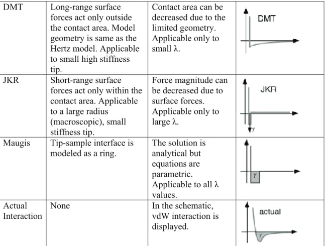
Model Assumptions Restrictions Schematics Hertz No Surface Forces Not applicable to
DMT Long-range surface forces act only outside the contact area. Model geometry is same as the Hertz model. Applicable to small high stiffness tip.
Contact area can be decreased due to the limited geometry. Applicable only to small λ.
JKR Short-range surface forces act only within the contact area. Applicable to a large radius
(macroscopic), small stiffness tip.
Force magnitude can be decreased due to surface forces. Applicable only to large λ.
Maugis Tip-sample interface is
modeled as a ring. The solution is analytical but equations are parametric. Applicable to all λ values.
Actual
Interaction None In the schematic, vdW interaction is displayed.
Table 1.1 Comparisons on the various contact adhesion models. For the definition of λ, see equation (1.3). γ is the work of adhesion. Schematics are from Carpick et al [40].
The Herz model assumes that there is no adhesive force between two objects, which
is not realistic. Considering the size of the tip and the stiffness of materials, the DMT model
fits well to my situation. I can check this with a parameter λ from the Maugis model. The
Maugis model can be applied to any situations, but the solution is analytical and depends on
a parameter λ. This parameter is an indicator of the closeness to a specific model. For
example, if λ is ∞, Maugis model becomes JKR model whereas if λ is 0, it becomes DMT
model. This parameter λ is defined by [39],
3 1 2 2 0 16 1 ⎟⎟⎠ ⎞ ⎜⎜⎝ ⎛ = K r π γ ξ
where ξ0 is the interatomic distance, r is the radius of the tip, γ is the work of adhesion, and K
is the effective Young’s modulus. K is defined by,
⎟ ⎟ ⎠ ⎞ ⎜ ⎜ ⎝ ⎛ − − − = E E K 2 ` 2 ` 1 1 4 3
1 ν ν
(1.4)
where ν and E are Poisson ratio and Young’s modulus for the graphite and Cr. The tip radius
was assumed to be same, 50nm. When ξ0 was set to 5Å and γ from the vdW energy, I have λ
= 0.15, close to the DMT model. From the DMT theory, the relationship between the forces
(external and surface force) and contact diameter, a is given by [36],
γ πR R
Ka
F = 3 −2 (1.5)
The DMT model assumes that there is an attractive force by adhesive energy, γ (second term
on the right hand side), and an external load, F (the term on the left hand side). Because my
devices experience no external load, I can set the force, F as zero. Then I have a = 3nm.
As a cross check, I also want to get the diameter from the Maugis model directly. The
equations in the Maugis model are expressed in terms of a parameter, m, which is an
indicator denoting how far the model is different from the Hertz model. If there is no
interaction between the two objects, m becomes 1; otherwise, it becomes larger than 1 [39].
[
]
⎥ ⎥ ⎥ ⎦ ⎤ ⎢ ⎢ ⎢ ⎣ ⎡ − − + − ⎟⎟⎠ ⎞ ⎜⎜⎝ ⎛ + − − + − ⎟⎟⎠ ⎞ ⎜⎜⎝ ⎛= 1 1arctan 1
3 4 1 arctan ) 2 ( 1 2
1 3 2 2
1 2 2 2 2 2 3 2 2 2 m m m r K a m m m r K a γ π λ γ π
λ (1.6)
[
2 1 2arctan 2 1]
3 2 2 2 3 − + − ⎟⎟⎠ ⎞ ⎜⎜⎝ ⎛ −
= m m m
r K a r Ka
F λ πγ (1.7)
Setting the external load, F = 0 in the eq. (1.7), I have two equations on the diameter, a, and
5nm. From the two models, the contact diameter is around 5nm. This information is used for
calculation of the vdW force in section 1.2.1.
1.4 Comparison of Surface Forces with Various Actuation Forces
and Their Scaling
1.4.1 Surface Forces between a Spherical Object and a Surface
To compare magnitudes of the above two adhesive forces with other types of forces
acting on an object, let me consider the forces between a spherical object and a plane. My
devices do not resemble a sphere, but the sphere model is the most simple for calculations
and makes comparisons easier on the relative magnitudes of the forces. Besides, any sharp
contact can be approximated by a spherical object. For comparison I will also calculate
electrostatic and gravitational force.
An approximate electrostatic force between a charged sphere and a conducting plane
is given by,
2 2
) 2 (
4 r
q Felec
πε
= (1.8)
where q is charge of the sphere, ε is the permittivity of the dielectric material (assumed to be
air, 8.85x10⁻¹²F/m), and r is the object radius. For the electrostatic force calculation, the
assumed surface charge density is ~2.6х10-5Cm-2 (discharge limit between conductive sphere
and uncharged conductive wall) [41].
g r Fgrav π 3ρAl
3 4
= (1.9)
where ρAl = 2700kgm-3 is the density of aluminum, g is the gravitational acceleration,
9.8m/s2.
The magnitudes of vdW and capillary force are already given in equation (1.1) and
(1.2) in section 1.2, so I will not repeat them here.
Figure 1.2b shows a comparison graph between forces assuming the same radius of
an aluminum sphere. Below 1mm, the dominating force is the capillary force followed by
vdW force. The electrostatic and gravitational forces are negligible. Based on the dominance
of the capillary force, I expect that the capability limitation of a MEMS device due to
adhesive and frictional forces will be very different depending on the humidity in the air and
the surface energy of absorbate liquid.
1.4.2 Scaling of Various Actuation Forces
Next, I want to consider dependencies of actuation forces on a characteristic
dimension, L of a MEMS system. Here I assume that a MEMS system is made of continuous
material, because, if a system size is larger than 10nm, the system can be treated by classical
mechanics as a continuum rather than a group of atoms. All intrinsic material parameters are
assumed to be constant. Extrinsic properties such as volume and mass scale by L3. A
description of scaling laws begins with a choice of a dynamical variable that does not scale.
Because I am dealing with forces, natural choices include constant mechanical stress and
constant electrostatic field strength. This implies a scale-independent elastic deformation, and
a scale–independent shape. Given stress and field strength, both the mechanical force and the
electrostatic force will scale with its cross-sectional area,
2
L area force
tic electrosta
force∝ ∝ ∝ (1.10)
Adhesion and friction scale with contact area,
2
L Friction
Adhesion∝ ∝ (1.11)
For a magnetic field I need to begin with voltage. Given a scale-invariant electrostatic field
strength,
L length field
tic electrosta
voltage∝ ⋅ ∝ (1.12)
1 − ∝ ∝ L area length
resistance (1.13)
Thus, the current will be,
2
L resistance
voltage
curent∝ ∝ (1.14)
Finally power laws of the magnetic field and magnetic force will be,
L distance
current field
magnetic ∝ ∝ (1.15)
4 2 L field) (magnetic area force
magnetic ∝ ⋅ ∝ (1.16)
The gravitational force depends on the mass,
3
L force nal
gravitatio ∝ (1.17)
From mechanical force and mass dependency, I have dependency for acceleration,
1 − ∝ ∝ L mass force on
accelerati (1.18)
To obtain frequency, I need to start from stiffness. Stiffness in shear or stretching yields,
L length
area
stiffness∝ ∝ (1.19)
1 − ∝
∝ L
mass stiffness
frequency (1.20)
Time is inverse frequency, so I have speed,
constant
= ⋅ ∝acceleration time
speed (1.21)
In small scale lubrication, reduction of a thickness of the lubricant layer increases shear rates
and hence viscous shear stresses,
1 −
∝ ∝
∝ L
thickness speed rate
shear speed
constant at
stress
viscous (1.22)
Finally, inertial force will depend on mass and acceleration,
2
L on accelerati mass
rce
InertialFo ∝ ⋅ ∝ (1.23)
Name Power Dependence on Length
Typical value (at 10nm)
Mechanical Force 2 10-7N
Adhesion & Friction 2 10-7N
Electrical Force 2 10-11N
Viscosity -1 10-11N
Inertia 2 10-13N
Magnetic Force 4 10-19N
Gravitational Force 3 10-20N Table 1.2 Scaling laws under classic continuum mechanics with characteristic magnitudes at L = 10nm. The typical force values from Drexler [42].
The power dependencies of the above quantities and their typical magnitudes at a
10nm length scale are shown in Table 1.2. Finally I want to compare the magnitudes of
surface force with various actuation forces. For that purpose, I calculated the forces in a
range of L from 10nm to 1mm. The mechanical force, for example, scales in the power of 2
beginning from 10-7N at 10nm according to Table 1.2. By the same method, all the forces are
calculated and plotted in Figure 1.4. One correction to the graph is for the strengths of the
adhesion and friction. For a 0.1mm3 object such as a dust particle on a surface, the adhesion
will be not be 10N as is indicated in Table 1.2, but will still be larger than the gravitational
force. For a 1mm3 object, the gravitational force becomes larger than adhesive force. Thus
the adhesion curve is deflected to match the gravitational force between 0.1mm and 1mm,
and the friction is assumed to be 1/10 of the adhesion throughout the whole scale. Based on
observation made in Figure 1.4, I can conclude that any force based on mechanical stress will
easily dominate adhesion. Thermal stress or electro-mechanical (i.e. piezo) stress are both
good candidates for micro-actuation. For free locomotive devices using an inertial impetus,
the inertial force will surmount the adhesion at a few tens of microns. If the inertial force
The gravitational force is too weak to work in the micro-regime. It only matches the
adhesive force to scales around 1mm. For this reason, gravity is rarely utilized in the MEMS
field. The magnetic force is a good candidate for a MEMS device when it is larger than
10μm, but it can be more useful in fluidic environments as the graph suggests. Viscosity
meets the magnetic force around a few hundred nanometers and this has been well
demonstrated by the manipulations of magnetic beads in liquids [43]. The electrostatic force
has a reasonable strength and many MEMS devices have been designed for this force.
1.5 Review of Actuators and Mobile Devices
Although there are numerous types of MEMS actuators, most share a common
attribute in their fabrication procedure as they are released from substrates after planar
fabrication processes complete. A micro-device is usually fabricated from a silicon or
polysilicon substrate in a micro-machining process. Although the fabrication techniques are
very diverse, the basic procedure for each includes: A sacrificial layer (often silicon oxide),
which is grown, or an etchable film is plated on top of a pure silicon wafer. Next, using
photolithography or electron beam lithography, desired patterns of metal films in the shape of
a final device are created. After a wet or a dry etching step the sacrificial layer underneath the
metal layer is removed so that the devices remain attached to the initial substrate by a
support. These attached structures are deformed (i.e. actuated) under a motive force.
There are very diverse kinds of actuators and I will only review briefly here the
thermal actuators as they are directly related to my actuation method. I can group actuators
by their materials or by application purposes.
By the definition of thermal actuation, materials that generate internal stress under
temperature variation are used for mechanical work. In U-shaped actuators, two monolayer
pieces of silicon or polysilicon, which have different cross sections, are joined at their ends.
Joule heating causes them to extend by different amounts [44, 45]. The unique property of
also widely used [46, 47]. Recently polymers have become popular in the fabrication of
novel micro-actuators as they provide better thermal expansion rates and accessibility to UV
(ultraviolet) and electron beam lithography. In the case of polyimide, the thermal expansion
coeffiient is known to be up to 25 times than best metal, Al [48]. Besides polyimide [49-53],
polypyrole [54-58], parylene [59], SU-8 [60] have also been used.
If I categorize thermal actuators by application, various kinds have already been
developed. For example, mirrors [61-63], conveyer systems [64-75], tweezers [60, 76-78],
ciliary system [70, 73-75, 79, 80], and fixtures [81, 82] have been demonstrated. Another
interesting application is the manipulation of a biological object in vivo or in vitro. In
particular, for the case of manipulating a living cell in a liquid environment, a stricter
limitation must be applied on the possible uses of the thermal actuators. Unlike in vitro
environment, thermal diffusion in liquid is stronger. Thus this kind of device requires much
more power to actuate. Additionally, the temperature of the actuator must be kept low
enough not to boil the liquid or to kill the cells [54, 57, 58].
Nanoscience has provided classes of novel micro-scale objects such as nanotubes and
nanorods. Their lengths are mostly in the range of tens of micrometers, and their sizes may
be useful in the fabricating of micro-actuators. This will enable micro-actuators, not only in
terms of actuation ranges but also for the sizes of the entire device. For example, a bimorph
is an actuating device, which uses differences of thermal expansion of at least two different
materials. Thus the length of the bimorph dictates the amount of deflection. Thus the
maximization of deflection based on the size limit of device is a primary concern. The
material stress. As I saw from Figure 1.4, the thermally induced mechanical stress is the
largest one among various force generating methods. It is therefore natural to choose the
thermal bending method for a miniaturized actuator.
The locomotive devices are the core topic of this thesis. A locomotive
micro-device is a MEMS micro-device that transforms physical or chemical energy into translation.
Fabrication of a locomotive device is more complicated because it has multiple fixed
actuators inside of it. Another term, micro-robot, indicates (albeit confusingly) a macroscopic
translation device. The term ‘micro-’ in their names means micron in volume, but not
necessarily in the length. I will confine the term, locomotive micro-device (or micro-robot) to
the devices that are smaller than a millimeter. This research field is currently active, but still
far from everyday life applications. Due to their compact size, the micro-robots can do useful
work in narrow regimes inaccessible to macroscopic tools. Based on this notion, many
possible applications have been suggested in several science/engineering journals [83, 84].
Traveling robots in future can collect, manipulate, and disperse smaller objects with
built-in actuators by remote control or under their own intelligence in fluidic environments or
on flat surfaces. As far back as several decades ago, typical examples have included the
traveling robots for repairing malfunctioned parts inside a machine and for detecting and
killing tumor cells inside a human body. However, due to the difficulties in miniaturization
of a self-actuating device and also in releasing process after fabrications to overcome surface
forces [85-90], this research field is still in a primitive state. Even so, there have been a
The scratch-drive-actuator (in short, SDA) developed by the Donald group uses the
elastic properties of the polysilicon films [91-95]. Since their actuators are electrostatically
coupled to one of a pair of conductive surface separated by a non-conducting layer, the
L-shaped film deforms itself so that contact area of the longer portion of the shape could be
varied repetitively. From the mechanical stress coming from longer portion, the tip of the
shorter portion slides a finite distance for every repetition (Figure 1.5). This kind of device
has already been developed to maturity and the most recent version is about 200μm long and
contains an additional arm to control its relative heading [95].
Another notable result in this field includes a swimmer; it consists of
micro-magnetic beads connected in series into a 20μm long oscillator [96]. Based on the magnetic
field strength variations, the bead chain waves so that the surrounding fluid can be repelled in
a given direction. By adjusting the strength of the oscillating magnetic field and the control
of elasticity of the chain, one can control swimming speed.
From this review, I now know that how small the realized devices are and what kind
of forces are employed in their actuation. If my research is meaningful in the context of
miniaturization history, my device can not be as large as a few hundred micrometers. Also I
want my device realized in a novel method of actuation. More importantly I address relative
strength of thrust compared to surface forces, which is not well treated in the SDA or
micro-swimmer research. I believe that the knowledge obtained in this research will be a first
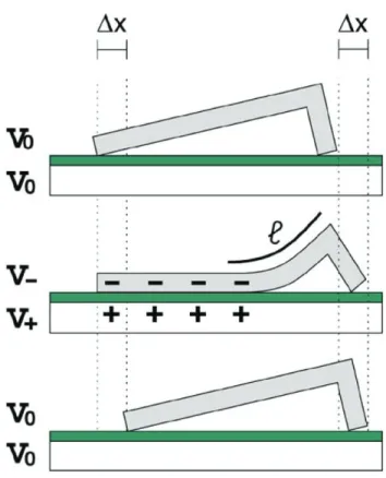
Figure 1.5 Schematic of the operation of a scratch drive actuator. At a parking voltage V0, the
SDA device stands without a deformation (top and bottom). The length of the curved region of the plate, l, and the step size, Δx, are determined by the actuation voltage, V+ applied on
the substrate. Figure from Donald et al [95].
1.6 Conclusion
I reviewed the types and relative magnitudes of surface forces and compared them
with various actuation forces. vdW force and capillary force are the most significant surface
forces. Among various actuation forces, inertial impact drive is a possible choice in our
research. From calculations, the inertial force would be larger than the surface forces above
10μm.
I estimated adhesion and friction per device. Adhesion per device will be 20nN and
the friction. I also reviewed the developments of various kinds of mobile devices. The
development of mobile device will greatly enhance capability of MEMS device. In the
context of development history of locomotive device, my research will be the smallest
Chapter 2 Locomotive Devices Driven by a
Radiometric Thrust and Estimations on
Thrust/Friction of HOPG Surface
2.1 Introduction to the Radiometric Effect
Although most of this research focuses on devices that use inertial impact as an actuation
method, it was also found that there is another mode of actuation, i.e. a radiometric thrust via
continuous laser illumination. Because both types of actuations are effective simultaneously
under certain conditions, I need to understand how the two mechanisms can be separated.
Also, radiometric thrust itself supplies another mode of translation. In this chapter, I will first
identify the conditions necessary to isolate one from the other. A critical power threshold
capable of driving a device in radiometric thrust is a good measurement for the estimation of
friction. Finally, translational motion will be demonstrated and some problems in actuations
will be addressed.
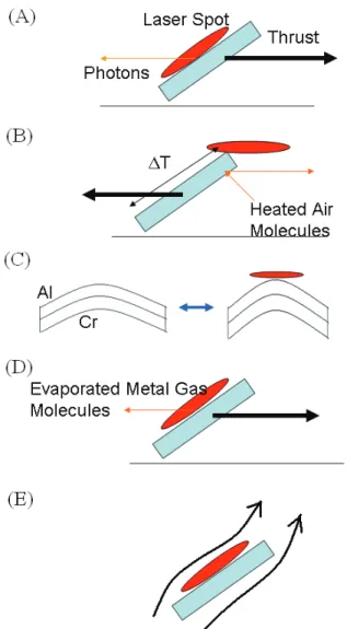
Light has been used to propel objects both in air and liquids. Five possible mechanisms of
force generation by light energy include photon momentum transfer, laser ablation, levitation
radiometric effect as a possible propulsion mechanism of my device. When light illuminates
an object, a temperature gradient is generated inside the object (Figure 2.1). Due to a
temperature gradient being present between an illuminated side and a non-illuminated side on
a device, air molecules bouncing from the illuminated surface will gain higher energy and
transfer relatively greater momentum than the ones from the non-illuminated side. Thus, a
net force is generated and this phenomenon is known as the radiometer effect, first
discovered by Ehrenhaft in 1918 [97]. The phenomenon has been used as a process of
particle collection in fluidic environments, although under a different name, photophoresis
[98-101]. In a typical experiment, a spherical bead is charged for levitation against gravity,
and it is heated laterally by a laser’s energy in a gaseous environment.
Though the magnitude of the force on a spherical bead is well known in free/forced gas
convective environments, there has not been any trial of utilizing this force for a locomotive
device until now. The radiometric effect has two following advantages. First, it enables fast
(on the order of 100μsec) temperature rise/fall in the supply and removal of energy to and
from a device. Second, a device is remotely controlled and does not require any additional
degree of complexity than a focused laser to generate a thrust. The photophoretic force
requires a temperature gradient across a device. Based on the simulations described below, I
am guided to fabricate devices with lateral dimensions in the range from 20 to 50 microns.
For successful propulsion, the applied force must overcome friction at the point of contact.
To minimize the friction, I have chosen a low friction substrate, HOPG as the playground for
Figure 2.1 Schematic illustrating the radiometric (photophoretic) effect.
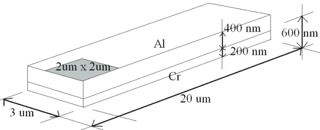
2.2 Fabrication (Common to Chapter 2 and Chapter 3)
2.2.1 Substrate Cleaning
The devices are thin metal films prepared on top of a silicon substrate. The silicon
wafer is a <100> crystal with arsenic doping. It had a 1µm-thick layer of oxide grown by
thermal baking when I bought the wafers from Virginia Silicon, Inc. A wafer was cut into
pieces in 3mm by 3mm with a diamond cutter. The wafer pieces are substrates to be used for
device fabrication via the electron beam lithograph. I did following cleaning steps before the
lithography step.
In a hood, the substrates were rinsed with acetone, methyl alcohol, and water for 10
seconds. After this, any remaining solution was blown dry by pressurized nitrogen gas. To
remove organic contaminants, the substrates were placed inside a plasma cleaner at 100W
alcohol, and water for 10 seconds each. The whole process described above was done twice
to remove contaminants completely.
A polymer based negative mask was used to selectively block metal evaporation. The
polymer was PMMA (polymethyl metharcrilate), and has a molecular weight of 1000,000. A
PMMA suspension was made in chlorobenzene, 8% by weight. Initial PMMA congregates
dissolved after several hours of sonication, resulting in a transparent viscous solution. Drops
of PMMA solution were pipetted onto the substrate to cover the surface. The PMMA
solution was then spin-coated by a rotational spin coater at 4000rpm for 40 seconds. To
evaporate the remaining chlorobenzene, the substrates were left on a hot plate for 5 min. at
170°C. After cooling the substrate in air, the substrates were ready for the electron-beam
lithography.
Figure 2.2 Schematics of device fabrication and transfer.
The electron beam lithography system is a combination of a field emission scanning
electron microscope (FE-SEM, S-4700, Hitachi) with a home-built lithography software,
called Seegerizer. The microscope has a resolution of tens of nanometers at 1000X zoom,
which is the required precision of this project.
2.2.2.1 Scanning Electron Microscopy (SEM)
The electron microscope uses an electron beam as a probe. The electrons are
generated by field emission from a heated filament cathode made of LaB6. Once the electrons
are ejected from the filament, they are accelerated by an electric field. Since the electron can
not pass through the air, the path of the particles must remain in vacuum inside the SEM
column. To prevent angular spreading of the beam and to focus it, apertures and
electromagnetic lenses are used. The aperture is a simple piece of metal with a hole, through
which the beam passes. When the aperture is in the middle of the beam with the hole at the
center of the beam’s axis, the divergence angle of the electron beam outside the beam path
will be limited. Thus a narrower beam spreading is obtained. The electromagnetic lens
generates a magnetic field to guide the motions of the electrons. The direction of the
magnetic field can be determined by the direction of the coil windings in the electromagnet.
To focus an electron beam, the coils are wound in a plane that is normal to the beam’s
direction. The generated magnetic field will be parallel to the direction of the electrons and
Faraday’s Law will force any stray electrons out of beam axis back to the axis. There are
three kinds of the electromagnetic coils; condenser lens coil, objective lens coil, and scanning
coil. The condenser lens is relatively weak lens and it determines the focused electron beam
beam diameter smaller. The objective lens generates a stronger field providing a focused spot
of the electron beam and also adjusts the focal distance. The final type is the scanning coil. It
determines the direction of the beam so that the focused beam spot can be laterally rasterized
just like the scan line on a television.
When the electron beam strikes surfaces of a specimen, not only are the electrons
adsorbed, but they are also ejected from the surfaces. The electrons emerging from a
specimen are collected by a positive electric field and fed into an electron detector. The
number of electrons collected per unit time will vary from location to location on the
specimen surface. Those differences generate an SEM image.
2.2.2.2 Electron Beam Lithography
The size of the electron beam spot is in the nano-meters range. The small size of the
spot can be used for fabricating nanometer scale objects. Instead of parallel scanning for the
beam in a rectangular frame, the scanning coil can be programmed to deflect the beam in a
desired pattern, thus ‘writing’ on a flat surface as if the beam were being used as a pencil. To
deposit solid materials selectively on a surface a mask is needed such as PMMA. The density
of the polymer in the solution determines the thickness of the spun layer. I used 8% PMMA,
which gave about 1µm thickness. When the polymer layer is exposed to accelerated
electrons, the long chains of the polymer molecule are broken, which makes them easier to
dissolve in a developer solution, a mixture of 1:3 by MIBK (methyl isobutyl ketone) and IPA
(isopropanol). After the lithography, an evaporated material will cover the whole substrate.
material on the bare exposed area will remain on the surface. For the removal of the polymer
layer, the substrate was rinsed in acetone for a 10min.
2.2.3 Seegerizer
The ‘Seegerizer’ software is a lithography tool enabling an SEM user to draw a
nanometer scale object on a silicon wafer. It is an interface between the electron microscope
and a computer. The Seegerizer controls the lateral motion of the electron beam by
controlling the strength of scanning coils in the SEM. As described in the previous section,
the SEM can scan in a rectangular shape just like the beam does on a TV screen. Each pixel
of the screen has a coordinates and this coordinates can be electrically converted to the
strength of the scanning coil current. When a user draws a geometrical pattern in the
rectangular screen, the Seegerizer software translates the coordinates into the control current.
Any arbitrary shape can be decomposed into simpler shapes such as a rectangle and a
polygon. A user can select a line, a rectangle, and a polygon in the software. Any rectangle or
polygon can be decomposed again into a collection of dots with some finite inter-dot distance
between them. Once the Seegerizer determines the location of each dot, it guides the
direction of the electron beam jumping from dot to next dot until all the dots are covered.
The degree of exposure or the amount of charge delivered to a dot is determined by
the dwell time and beam current. The dwell time is an amount of time that determines how
long the electron beam will stay at a dot. The longer the beam stays in one place, the more
charge is delivered. The beam current is the number of electrons per unit time arriving on the
surface of the sample. Before any exposure, an SEM user is required to calibrate the beam
passes them to a pico-Amp meter. The user can determine how much charge will be
transferred to a unit area or unit path length by typing an arbitrary number in the Seegerizer
window. If the number is given, Seegerizer can calculate the dwell time for each dot.
The advantage of the Seegerizer over other lithography software (e.g. NPGS (nano
pattern generator system)) is that it has versatility in aligning edited patterns on a pre-imaged
area. One difficulty of the electron beam lithography is that once the silicon wafer is covered
by a PMMA layer, one can not image delicate features on the silicon surface. Only large and
thick structures like patterned Au-Cr layers more than 100nm thick can be imaged under the
polymer layer. If there is any big landmark such as an Au-Cr pattern, the Seegerizer can use
it as a reference mark to align the desired patterns. If an alignment is needed, the user takes
images of the intended exposure area before the area is covered by PMMA layer, and uses it
as a reference. If such the alignment step is not required, the Seegerizer can be used as a free
drawing tool. Below are the parameter inputs frequently used in the lithography.
Name of Parameter Value Units
Beam Current 19 pA
Dot Spacing 20 nm
Line Spacing 50 nm
Figure 2.3 Screen capture of Seegerizer edit window
2.2.3 Metal evaporation and Lamination on substrates
A thermal evaporation system from CVC (consolidated vacuum company) developed
in 1960’s was used to evaporate metals. The materials used were Al, Cr, and Au. The crystal
thickness monitoring system had a resolution of a few nm. The vacuum levels were kept
under 10-5 Torr before evaporation and were maintained at a similar level during evaporation.
The evaporation rates were about 100Å/sec for Al, 2Å/sec for Cr, and 5Å/sec for Au,
although the evaporation rate is not of great importance. The thickness of each film however
was more important ensuring uniformity of a device’s deformation under a temperature
variation. The thickness of Al was 400±10nm, 200±10nm for Cr, 5±5nm for Au, nominally.
All of MEMS devices are separated by silicon surfaces by one of several etching
techniques. The etching techniques can be divided broadly into two categories, wet and dry
etching. For isotropic wet etching, hydrofluoric acid (HF) is commonly used. The three most
important anisotropic silicon etchants are potassium hydroxide (KOH), ethylene diamine
pyrochatechol (EDP), and tetramethyl ammonium hydroxide (TMAH). These etchants attack
silicon along preferred crystallographic directions. The crystallographic plane showing the
slowest etch rate is the <111> plane, while the fastest etch occurs into the <100> plane.
Dry etching has several advantages compared to the wet etching techniques. These
include smaller undercut regions and higher anisotropy. However, selectivity in dry etching
is lower than it is with wet etching. The three basic dry etching techniques; high-pressure
plasma etching, reactive ion etching (RIE), and ion milling, utilize different mechanisms to
obtain directionality. Ion milling is a purely physical process, which utilizes accelerated inert
ions (e.g. Ar+) striking perpendicular to the surface to remove material. In high-pressure
plasma etching, highly reactive species are created that react with the material to be etched.
The products of the reaction are volatile so they diffuse away and new materials are exposed
to the reactive species. RIE etching, also called ‘ion-assisted etching’, is a combination of
physical and chemical processes. In this technique, the reactive species react with the
material only when the bonds of surface materials are broken by the collision of incident ions
from the plasma. The directionality of the ion’s velocities produces many more collisions
with the horizontal surfaces than with the walls, thus generating faster etching rates in the
vertical direction.
In my research, wet etching techniques need to be avoided because of the fluidity of
can exert unnecessary force causing devices to stick to the substrate while drying. I used a
reactive ion etching machine (SAMCO RIE) to peel our devices off of silicon oxide surfaces.
C3F8 gas was used as the etching agent with a flow rate 1.2cc/min. in 8 minutes, 110W
power. The dry etching technique initially appears undesirable when considering that there is
no undercut beneath the patterned metal devices. However, after the etching step, it was
found that roughly 50% of the metal films were curled up from the tip of their spokes.
Although dry etching is nominally normal to the surface, some of the etchant gas molecules,
C3F8, approach the interface of the Au and silicon oxide to initiate separation between the
two surfaces. Once a gap starts at the tip of the spoke, the internal metal stress at the spoke
raises the separated portion causing the observed curling at the tip. This process continues
until the entire portion of the spoke is raised completely except for the center portion that is
barely held by the remaining oxide pillar. This can be supported by the observation that the
sharp tipped spokes are peeled off more easily than the rectangular-ended spokes.
Of course not all of the patterned metal shapes are easily peeled away. Because the
curling process depends on the internal stress of the metal films, if the width of a film is too
narrow compared with the total length of a pattern, the film will be remained attached to the
surface. If the width is too wide, the curling will happen in an unintended direction. To verify
this, an experimental peeling test was done with various aspect ratios (Figure 2.5). The SEM
picture teaches two lessons. First, given a finite width, there is a ‘limit’ on the separation
length from the tip of a rectangular pattern (far right column in Figure 2.5). Identical peeling
depth is clear in all of the metal films that have various lengths with a constant width.
Second, for a complete separation, there is an optimum aspect ratio, about 1/7~1/6 in length
versus width (center column in Figure 2.5). Following this rules, I designed all the spokes of
the devices to have similar ratios to produce efficient peeling.
This assisted peeling process by dry etching has not yet been reported in any
publication, and the exact conditions for better peeling are not studied in depth in this
research. Optimization research on this topic should be focused on in future studies.
2.2.5 Internal Stress of Thin Metal Films
It is well known that the internal stress of thin metal films change under a temperature
cycle [102, 103]. Al [104] and Cr [37] films also experience the variations in the stress
through baking. The amount of stress variation depends on the maximum temperature
achieved during the first baking process. The larger the temperature variation from room
temperature, the more stress variation in the film (The first and second thermal cycles in
Figure 2.6). After cooling to room temperature, the stress change becomes permanent, and
becomes more tensional or compressional depending on metal species. Once the film
experienced a saturated permanent stress change, no further baking could induce additional
changes, only retracing the same stress curves under subsequent temperature cycles (third
and fourth thermal cycles in the Figure 2.6). This is true even when the baking temperature is
set higher once the saturation is achieved.
The change in film stress due to baking temperature can be a convenient method for
controlling an initial curvature of the devices. After the etching step, if the curvature of a
device is too large and the device is relatively flat, the substrate containing the device was
put into a tube furnace and baked in air. The temperature range was between 300~500°C
above room temperature. Angled SEM pictures verified the variation of the curvature. If the
change is not enough, more baking was done by setting a higher temperature in the furnace.
This method was used when the length of the spokes in a device is relatively short (circa
Figure 2.6 Schematic interpretation of the stress variation graph from Hu et al [37]. Starting from an initial stress it undergoes permanent change through first thermal cycle. From the second thermal cycle the stress comes back to its previous newly naturalized value.
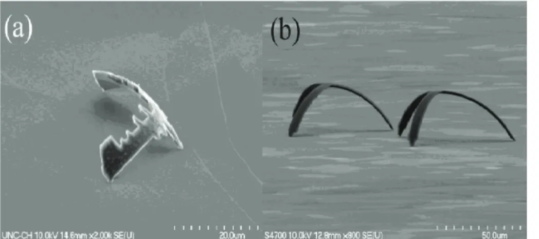
Figure 2.7 Adjustment of an initial curvature with a test device. The claws are made of Al-Cr double layer metal films. Each picture was taken at room temperature after one cycle of temperature change. (a) Right after etching. (b) Furnace set to 50°C (c) Furnace set to 100°C (d) Furnace set to 150°C (e) Furnace set to 200°C (f) Furnace set to 250°C (g) Furnace set to 300°C (h) Furnace set to 400°C (i) Furnace set to 700°C
A freshly cleaved HOPG sheet was prepared from a piece of HOPG (purchased from
GE Advanced Ceramics, pyrolytic graphite, ZYA or ZYB Grade, 12mm by 12mm by 2mm)
and used as provided. To cleave a thin film of HOPG, a thin-film sticky tape was prepared
and attached on one side of the graphite block in the direction parallel to the graphite’s basal
plane. Peeling the tape off by hand caused a few layers of HOPG to be separated, providing a
fresh surface. The fresh surface was used for the device playground without any surface
modification.
The tape-HOPG sheet covered the silicon substrate. A PDMS (polydimethyl siloxane)
block was prepared in advance and it was put on top of the HOPG sheet. A gentle press
caused the devices to be transferred onto the HOPG by surface forces acting on the spoke tips
of the devices. When the devices were transferred they stood with a convex posture (Figure
2.8). Not all of the devices on the silicon substrate were transferred and some devices were
broken due to pressure, but some reached clean plateaus of HOPG safely. The overall
transfer success rate of a batch, staring from the lithography step, was 10%, but the process
itself was found to be highly repeatable, allowing any number of devices to be obtained.
2.3 Experiment Setup
Figure 2.9 is a schematic for the optics setup used for actuating experiments. A
180mW laser was used to control a device’s temperature. For visual alignment of a focused
laser spot, a CCD camera was used, and for illumination of the substrate, a light bulb was
used. Instead of adjusting the locations of the lasers, the substrate was translated by an XYZ
stage manually or by a piezo control unit if a fine control of translation is needed.
When a vacuum environment was required, a home-built vacuum chamber was used.
The HOPG substrate was attached inside of it, and a glass cover was used to seal the chamber
but the background light and lasers can pass through the glass window. I used a mechanical
pump and a diffusion pump, which can pump down to 10-4Torrs for a vacuum environment.
The vacuum tests in this thesis imply the air pressure level below 10-3Torr.
For the driving of the devices against frictional forces, the power of the actuating
laser (L1 in the schematic) becomes important. To keep the amplitude at a maximum
throughout the optics setup, polarizing beam splitters were used. Among three beam splitters
used in the schematic, BS1 and BS3 were polarizing beam splitters, which have a preferred
beam passing orientation and a polarization plane, so that it allows more than 90% of the
incident power of the actuating laser to pass. As a result, the laser power directly impinging
on the devices was 20±2mW maximum in continuous mode. BS2 is a non-polarizing beam
splitter, which passes 50% of power in any direction and polarization so that the CCD camera
Figure 2.9 Optics schematics used for control and monitor of curvature of the devices.
Item Catalog Company
Laser 1 (L1) DL7147-201, 660nm,
180mW Thorlabs Laser Controller LDC2000 Thorlabs Objective Lens M Plan Apo 50 Mitutoyo Beam Splitter (Non
Polarizaing) U47-122 Edmund Optics Beam Splitter (Polarizing) P47-125 Edmund Optics
XYZ Stage 360-90 Newport Piezo Control Unit MDT 690 Thorlabs
Pulse Generator 8005B Hewlett Packard CCD Camera WAT-902C
HOPG Grade ZYA, ZYB Advanced Ceramics Table 2.2 Parts list
2.4.1 Candidate Theories to Explain the Motions
In theory, there are 5 possible candidate mechanisms; the radiometric effect, photon
momentum transfer, inertial impact drive by repeated thermal modulation, ablation, and
pneumatic pressure by a free heat convection.
Before discussing the proof of a particular mechanism, I will review the principles of
each mechanism briefly. According to Planck’s well known theory of the quanta of light
[105], the particles called photons have momentum like any other materialistic particles such
as protons and electrons. They move straight in space and at the surface of an object, some
portions of the photons are absorbed in the form of heat energy, while the rest of them are
reflected. When they rebound, their momenta are transferred like colliding macroscopic balls.
Thus the illuminated object gains the same amount of momentum. Although a momentum
transfer from one single photon is tiny, if the number of photons is enormous, the sum of
their momenta cannot be ignored. In my experiment, friction of nano-contacts between a
device and graphite will be on the order of nN, so there is a possibility for the photons to
drive our devices. According to the LFM (lateral force microscopy) studies done in air on
HOPG [106, 107], the magnitude of friction on graphite from point tips of AFM cantilevers
is various from 100pN to 1nN. The momentum of a light particle, p, is given as,p=E c,
where E is the energy and c is the speed of light. The energy of the laser that directly hits the
surface of our device is about 20mW, which gives about 30pN. This number is a little bit
smaller than the friction expected, but there is still room for the possibility of locomotion via
momentum transfer.
Because an introduction to the radiometric effect is already presented in section 2.1, it
numerically how large the thrust will be by a finite element analysis simulation study when
the power of the laser is known.
Another strong candidate is the thermal modulation. As was described in the
introductory chapter, my devices have two different metal films attached to each other. I used
Al and Cr among other metals for their greatest differences in their thermal expansion
coefficients. Thus, depending on the temperature change, the curvature of the bimorph will
modulate. The estimated thrusts will be given in chapter 3, but the magnitude is well above
the HOPG friction. Instead, the primary concern is the role of the contact tips. It is not
expected that the cantilever’s full deflection force will be used to push/pull a device, but it is
expected that primarily the contact tips will slide on the surface. Only tiny fractions of this
force will be used in an actuation.
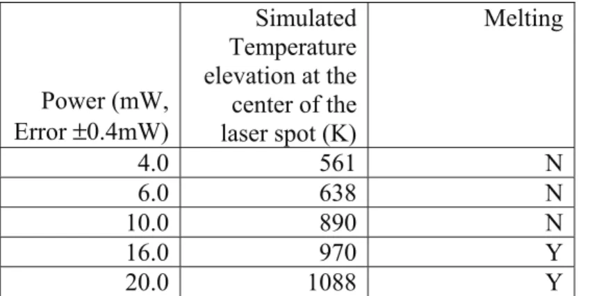
The energy of the laser can quickly raise the temperature to the melting temperature
of Al (933K) and my devices are basically thin films rather than a bulk. As a result, the actual
melting temperature can be a lot lower than melting point of bulk for both Al and Cr. If a
metal surface melts down, the evaporated gas will gain momentum. Thus by the Newton’s
third law, the device will gain momentum.
Finally, pneumatic pressure can be another candidate. Due to heating of the
surrounding air molecules energized by a hot metal surface, the air flow speed of the top and
bottom sides will be different. By Bernoulli’s principle, a pressure difference attempts to
levitate a device. Usually, the body of the device has a slope angle against the substrate and
Figure 2.10 Five possible mechanisms: (a) Photon momentum transfer (b) Radiometric effect (c) Inertial impact by repetitive thermal modulation (d) Ablation (e) Air pressure difference generated by natural heat convection.
2.4.2 Examinations of Each Mechanism
I will examine each candidate theory one by one under different conditions. The first
one I will consider is the pneumatic pressure. The magnitude of the pneumatic pressure will
be ( 2 2 )
2 1
bottom top v
v
p= −
Δ ρ from the Bernoulli’s equation, where Δp is the pneumatic pressure
difference between the top and bottom of a device surface, ρ is density of air per unit