٭Corresponding Author, Email: [email protected]
Reducing the Power Consumption in FlashADC using
65nm CMOS Technology
N. Haji-Karimi1 and M. Dosaranian-Moghadam2*
1- M.Sc. Educated, Department of Electrical, Biomedical and Mechatronics Engineering, Qazvin Branch, Islamic Azad University, Qazvin, Iran
2- Assistant professor, Department of Electrical, Biomedical and Mechatronics Engineering, Qazvin Branch, Islamic Azad University, Qazvin, Iran
Received 21 September 2015, Accepted 2 January, 2016
ABSTRACT
Today, given the extensive use of convertors in industry, reducing the power consumed by these convertors is of great importance. This study presents a new method to reduce consumption power in Flash ADC in 65nm CMOS technology. The simulation results indicate a considerable decrease in power consumption, using the proposed method. The simulations used a frequency of 1 GHZ, resulting in decreased power consumption by approximately 90% for different processing corners. In addition, in this paper the proposed method is designed using an interpolation technique for the purpose of promoting the performance as well as decreasing the class of Chip. The simulation results indicate that the power consumption for the interpolation technique is decreased by approximately 5% compared to the proposed method. On the other hand, we compare the results of the proposed convector with those of convertors frequently referred in other studies. Also, the results show that the power consumption is considerably decreased, using the proposed method.
KEYWORDS
Vol. 48, No. 1, Spring 2016
38
1. INTRODUCTION
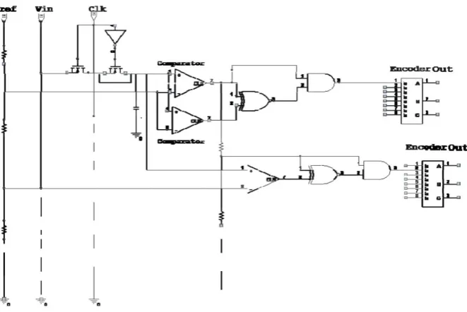
Due to their flexibility and simplicity, digital systems and signals processing are preferred over analog ones in today's processing world even though our surrounding environment is characterized by analogue properties. Today, designing ADC is emphasized given the extensive use of convertors in telecommunication systems and electronics and control systems as well as the advantages emanating from the use of digital signal processing. These advantages have inspired the researchers and manufactures to use Integrated Circuits (IC) in making and developing convertors. Due to its high integration capability, low power consumption and low price, CMOS technology is commonly used to design ADC, with low power consumption considered as the first priority. As Flash ADC enjoys simplicity and high speed, it is widely used in systems [1-3]. In [4], a 400-Msample/s, 200 mW CMOS device, and in [5], a 350-Msample/s BICMOS device were described. However, there are additional applications in the wireless area coming up, where only a flash ADC gives sufficient accuracy at the required large analog bandwidth, for example in ultra-wide-band systems [6].
A combination of convertor speed, number of Bit and power consumption indicate the quality of convertor. However, in many cases, power consumption by itself is an indicator of the quality. Encouraged by the extensive use of data convertors in widely used systems such as telecommunication systems, videos, Television, wireless systems, the researchers have sought to decrease the power consumption so that the use of a convertor with high speed and low power consumption has turned into a research focus [7-10]. It has the speed advantage of the flash ADC, while the number of comparators is greatly reduced with analog pre-processing. As an ADC and because of its high speed and simple circuit, Flash convertor is commonly used in industry. Due to their high speed, simple circuit and parallel processing capability, Flash convertors are preferred over other types even the former are less accurate. However, reducing the power consumption is the main challenge faced by the researchers. This study presents an applied method aiming at reducing the power consumption in Flash ADC. Fig. 1 shows a conventional flash ADC [11]. As this figure shows, the Flash convertor consists of 3 main components: resistor string, comparator, and Encoder. The number of resistor strings is 2 and the number of comparators is 2 −1 for an -Bit output. In flash convertor, the comparisons conducted by comparator are transmitted to thermometer to binary code convertor and converted into a binary code. The (2 −1 ) encoder also
converts its input thermometer code to bit binary code. Initially, the comparator compares the input voltage ( ) against the reference voltage , , where =
1, 2, … , 2 −1, on the resistor ladder. Then, the comparison results( )are transmitted to thermometer of the binary code convertor. The downsides of this circuit include kick back noise, bubble error, large volume of hardware and high power consumption. The kick back noise and bubble error are removed by inserting pre amplifier and AND-OR logical gates in the circuit, respectively.
In this paper, we show that the interpolating technique is useful for the power consumption in CMOS technology. Section 3 describes the proposed method. Section 4 will present the simulation results contained by the proposed method and interpolation technique. Finally, some conclusions are provided in Section 5.
Fig. 1. Conventional flash ADC architecture [11]
2. REVIEW OFINTERPOLATIONTECHNIQUE
The attractive feature of interpolating ADC is that high speed sample and hold amplifier is optional due to parallel operation of fine and coarse converter. The circuit interpolation technique can be used to reduce the volume of hardware. Recently, interpolation has been widely used to reduce the power consumption and chip class and hence the costs. The proposed method draws on interpolation for the purpose of reducing the hardware volume and power consumption. On the other hand, capacitive interpolation uses a purely reactive averaging network between the outputs of adjacent amplifiers [6]. Fig. 2 shows how this technique is implemented. For example, in an bit flash convertor, there will be2 −1 comparator numbers to be reduced, based on the circuit distortion technique which works as follows: It uses alternately the resistance voltage division instead of preamplifier. Due to its high speed, accuracy and low volume as well as its simplicity of circuit, this technique is very popular [11-13].
convertors in electronic devices and the industries such as medical science, telecommunication and military have brought the researchers and users' attention to the necessity of reduction in power consumption. The recent years have seen the rapid development of ADC hardware as well as digital signals processing. The power consumption indicates the extent to which power is used in various blocks of a circuit. The consumption of more power leads to both higher price and a decrease in circuit life cycle. This study aims to offer a method to reduce the cost and power consumption as well to increase the life cycle of the convertor [14-21].
Fig. 2. Interpolation technique [1-2]
Generally, the power consumption is divided into two categories: 1- dynamic, 2- Static. The dynamic power results from the power consumed in sampling time, the power consumed due to external disturbing factors and the power consumed as a result of circuit offset. The static power results from the power consumed due to charge injection and the power consumed by voltage source. Literature on convertors shows the role of convertors calibration in reducing the power consumption. This is achieved by reduction in comparators offset through the proper design of transistors [1, 2]. Memory block is a component of comparator circuit which holds and transmits the data to the output. The method proposed by
this study decreases the power consumption by removing comparators memories and calibration. Fig. 3 shows how memory is removed from comparator. A logical procedure is used to meet the goal and to control the timing of the circuit, thereby its duty namely the maintaining and transmitting the data to the output is performed, followed by the arrival of the next clock.
Flash convertor has a high speed which in turn depends on the comparator speed. The comparators are made, using the technology of integrated circuits. However, the speed of integrated circuits depends on transistors dimensions. Therefore, transistors dimensions influence the speed of comparators which, in turn influence the speed of the flash convertor. The 65nm CMOS technology used in the proposed method decreases the dimensions on transistor scale. This increases the speed of integrated circuits performance, leading to a decreased power consumption by decreasing the dimensions and advanced technology. Input signal in flash convertors is periodic, continuous and changing and it is addedto the circuit in a given time range step by step for the purpose of properly being processed. A sample and hold circuit based on charge injection is used at the beginning of the circuit for achieving proper timing and sampling improvement. This solves the clock Feed through and charge injection problems. As a result the power consumed due to the leakage current is reduced. Being a comparator, XNOR gate is used to ensure the reliability of comparators output results. This gate is selected among other gates because of its performance at the time when the outputs of both comparators are equal. If both inputs of this gate are equal, the output would be
"1" amount which is compatible with comparators performance. Moreover, AND gate is used to increase the reliability of the proposed circuit
Vol. 48, No. 1, Spring 2016
40
3. PROPOSED TECHNIQUE
In this section, we describe the proposed method for the power consumption in 65nm CMOS technology. Fig. 4 shows a level of the circuit designed based on the guidelines described in section 2. The performance of the proposed circuit at the time when the input signal is to be sampled is the comparator compares the voltage obtained from the sample against the reference voltage. The results of both comparisons are applied to XNOR gate for the purpose of ensuring the reliability of the results. The AND logical gate is also used to meet the duty of memory followed by the arrival of next clock. This process also reduces the power consumption and increases the reliability of the system. The interpolation technique is used to decrease the class of chip as well as prices (see Fig. 5). The performance of this circuit is similar to that of the circuit given in Fig. 4. But in the former the
comparator is removed alternately and the resistor voltage division is used to meet the circuit performance. This downgrades the class of chip and hence the price of circuit design.
4. SIMULATIONRESULTS
This section deals with the performance of the proposed method and interpolated circuit and compares it with the commonly used methods. The simulations are conducted using flash ADC with a 3 bit accuracy and sampling frequency of 1 GHZ in 65nm CMOS technology. The following section compares the proposed convertor with those designed in [22-24].
Table 1 shows the simulations results for the proposed method and the designed circuit interpolation in comparison with the conventional method for various processing corners and different temperatures. As Table 1 Fig. 4. The removing the memory of the comparator circuit [14]
shows, the power consumption is reduced to 16.81mW, using the proposed method for the TT corner and temperature 60℃. This indicates a decrease in power consumption by approximately 153mW in comparison with the conventional method. It can be also observed that the power consumption using the interpolation technique is lower than that with the proposed method. On the other hands, Table 1 shows, the use of the proposed method and interpolation technique lowers the power consumption by approximately 148mW and 150mW for SS corner and temperature 90℃, respectively in comparison with the conventional method. In addition, compared to the conventional method, the power consumption will be lowered to by approximately 138mW and 141mW for FF corner and temperature−40℃, using the proposed method and interpolation technique, respectively. Table 1 further shows that using the proposed method at the TT corner and temperature 60℃ leads to a more reduction in the power consumption than the reduction obtained for other corners. This had been predicted given the transistors switching in good conditions. The maximum reduction in power consumption at the TT corner in comparison with the conventional method indicates that the Effective Number of Bit has approached the nominal 3 Bit, indicating the decreased Figures Of Merit (FOM), using the proposed method. It should be mentioned that the FOM is one of the main criterions for selection of convertor. This criterion indicates the extent to which the system performance as well as electronic components catch up with technology advancement. The lesser the power consumption, the lower FOM. The FOM is calculated as [1]:
FOM = TotalPower/(2 − ) (1)
where and are bits and sampling frequency of the convertor, respectively.
TABLE 1. THE POWER CONSUMPTION FOR THE PROPOSED CONVERTERS AND CONVENTIONAL METHOD
AT DIFFERENT PROCESSING CORNERS
Converter
Power Consumption for FF Corner
and Temperature
− ℃
Power Consumption for SS Corner
and Temperature
℃
Power Consumption for TT Corner
and Temperature
℃
Conventional
Converter 155.3mW 164.6mW 170mW
Proposed
Converter 17.19mW 16.07mW 16.81mW
Proposed Converter with
Interpolation Technique
14.17mW 13.78mW 13.81mW
Comparing the proposed methods with the conventional method, Table 2 shows the FOM for different processing corners. According to this Table, by using the proposed method and convertor interpolation, the FOM is improved compared to the conventional method. It can also be seen that the FOM in the proposed converter with interpolation technique is lower than that in the proposed method. On the other hand, we observe that the FOM is reduced maximally at the TT corner in comparison with the other processing corners. Fig. 6 also shows the FOM for the proposed method, convertor interpolation, and conventional method at three processing corners.
TABLE 2. THE FIGURES OF MERIT FOR THE PROPOSED METHODS AND THE CONVENTIONAL METHOD AT
DIFFERENT PROCESSING CORNER
Converter
FOM for FF Corner and Temperature
− ℃
FOM for SS Corner and Temperature
℃
FOM for TT Corner and Temperature
℃
Conventional
Converter 21.25× 10 20.57× 10 19.41× 10 Proposed
Converter 2.10× 10 2× 10 2.14× 10 Proposed
Converter with Interpolation
Technique
1.72× 10 1.72× 10 1.77× 10
Fig. 6. The figures of merit for the proposed methods and the conventional method at three processing corners
Vol. 48, No. 1, Spring 2016
42
reduced depends on the accuracy, speed and the type of the technology used.
TABLE 3. COMPARING THE PROPOSED CONVERTOR WITH THE PROPOSED CONVERTOR IN REFERENCES
[22-24]
Converter Frequency TSMC Bit Power
Consumption
Reference [22] 20 MHZ 0.18 3 36.273 mW
Reference [23] 20 GHZ 65nm 3 5.1W
Reference [24] 1.2GHZ 180 4 86mW
Proposed Method 1 GHZ 65nm 3 16.81mW
5. CONCLUSIONS
In this paper, we proposed a new method for reducing the power consumption in 3 bit ADC in 65nm CMOS technology. It has been shown that the power consumption becomes much lower, using the proposed method in comparison with the conventional method. Moreover, convertor interpolation method was used to improve the performance of the proposed convertor, resulting in the reduced power consumption of the convertor. On the other hand, it has been shown that the power consumption for the TT corner is decreased in comparison with that the SS and FF corners. It has also been observed that the FOM in the proposed methods is lower than that of the conventional method. Our results have also showed that the proposed convertor designed by technology 65nm, an increases speed by decreases hardware volume and leads to a reduction in power consumption by approximately 90%.
REFERENCES
[1] B. Razavi, Principles of Data Conversion System Design, Wiley-IEEE Press, 1994.
[2] D. Johns and K. Martin, Analog Integrated Circuit Design, John Wiley &Sons. Inc, 1997.
[3] A. Agarwal and J. Lang, Foundations of Analog and Digital Electronic Circuits, Elsevier. Inc, 2005.
[4] S. Tsukamoto, T. Endo, and W. G. Schofield, "A CMOS 6b 400 Msample/s ADC with error correction," in Proc. IEEE Int. Solid-State Circuits Conf., pp. 152-153, Feb. 1998.
[5] P. Setty, J. Barner, J. Plany, H. Burger, and J. Sonntag, "A 5.7b 350 Msample/s or 6.75b 150 Msample/s Reconfigurable Flash ADC for a PRML Read Channel,"IEEE Int. Solid-State Circuits Conf., pp. 148-149, Feb. 1998.
[6] C. Sandner, M. Clara, A. Santner, T. Hartig, and F. Kuttner, "A 6-bit 1.2-GS/s Low-Power Flash-ADC in 0.13 m Digital CMOS,"IEEE Journal of Solid-State Circuits, Vol. 40, No. 7, pp. 1499-1505, July 2005.
[7] B. Brandt and J. Lutsky, "A 75-mW 10-B 20-Msample/s CMOS Subranging ADC with 59-dB SNDR,"in ISSCC Dig. Tech. Papers, pp. 322-323, Feb. 1999.
[8] A. Dingwall and V. Zazzu, "An 8-MHZ CMOS Subranging 8-bit A/D Converter,"IEEE J. Solid-State Circuits, Vol. SC-20, pp. 1138-1143, Dec. 1985.
[9] A. Abo and P. Gray, "A 1.5-V 10-bit 14.3-MS/s CMOS Pipeline Analog-to-Digital Converter," IEEE J. Solid-State Circuits, Vol. 34, pp. 599-605, May 1999.
[10] K. Nagaraj, H. S. Fetterman, J. Anidjar, S. H. Lewis, and R. G. Renninger, "A 250-mW 8-b 52-MSample/s Parallel-Pipelined A/D Converter with Rduced Number of Amplifiers,"IEEE J. Solid-State Circuits, Vol. 32, pp. 312-320, 1997.
[11] Chun-Cheng Huang, "A Background Comparator Calibration Technique for Flash Analog-to-Digital Converters," IEEE Transactions On Circuits And Systems, Vol. 52, No. 9, pp. 1732-1740, Sept. 2005.
[12] W. Kester, Analog to Digital Conversion,Elsevier, 2004.
[13] Marcel J. M. Pelgrom, Analog-to-Digital Conversion, Springer Science, 2010.
[14] F. Maloberti, CMOS Comparators, University of Pavia, 2009.
[15] Jyun-Syong Lai and Zhi-Ming Lin, "A 6-bit 2GS/s Low Power Flash ADC," International Journal of Engineering and Technology (IACSIT),Vol. 4, No. 4, pp. 369-387, August 2012.
[16] M. Panchore and R. S. Gamad, ''Low Power and High Speed CMOS Comparator Design using 0.18 μm Technology,'' International Journal of Electronic Engineering, Vol. 2, No. 1, pp. 71-77, 2010.
[17] P. Sunghyun, Y. Palaskas, and M. P. Flynn, ''A 4 GS/s 4b Flash ADC in 0.18μm CMOS,''IEEE Journal of Solide-State Circuits, Vol. 42, No. 9, pp. 1865-1872, Sept. 2007.
[18] S. S. Khot, P. W. Wani, M. S. Sutaone, and S. Tripathi, "Design of a 45nm TIQ Comparator for High Speed and Low Power 4-Bit Flash ADC," International Journal on Electrical and Power Engineering (ACEEE), Vol. 2, No. 1, pp. 7-10, Feb. 2011.
[20] S. Oza and N. M. Devashrayee, "Folding & Interpolating ADC using Low Power Folding Amplifier," International Journal of Electronics & Communication Technology (IJECT), Vol.1, No. 1, pp. 49-54, Dec. 2010.
[21] C. Lane, "A 10-Bit 60 MSPS Flash ADC," IEEE Bipolar Circuits and Technology Meeting, pp. 44-47, Sept. 18-19, 1989.
[22] P. Kumar and A. Kolhe, "Design & Implementation of Low Power 3-bit Flash ADC in 0.18μm CMOS," International Journal of Soft
Computing and Engineering (IJSCE), Vol.1, No. 5, pp. 71-74, Nov. 2011.
[23] D. Ferenci, M. Grozing, F. Lang, and M. Berroth, "A 3 bit 20 GHZ Flash ADC in 65 nm Low Power CMOS Technology," Proceeding of 5th European Microwave Integrated Circuits Conference (EUMA), Paris, France, pp. 214-217, Sept. 27-28, 2010.
![Fig. 1. Conventional flash ADC architecture [11]](https://thumb-us.123doks.com/thumbv2/123dok_us/8944500.1853868/2.595.312.539.327.452/fig-conventional-flash-adc-architecture.webp)
![Fig. 2. Interpolation technique [1-2]](https://thumb-us.123doks.com/thumbv2/123dok_us/8944500.1853868/3.595.108.487.566.756/fig-interpolation-technique.webp)