16‑Channel biphasic current‑mode
programmable charge balanced neural
stimulation
Xiaoran Li
1, Shunan Zhong
1*and James Morizio
2*Abstract
Background: Neural stimulation is an important method used to activate or inhibit action potentials of the neuronal anatomical targets found in the brain, central nerve and peripheral nerve. The neural stimulator system produces biphasic pulses that deliver balanced charge into tissue from single or multichannel electrodes. The timing and amplitude of these biphasic pulses are precisely controlled by the neural stimu-lator software or imbedded algorithms. Amplitude mismatch between the anodic current and cathodic current of the biphasic pulse will cause permanently damage for the neural tissues. The main goal of our circuit and layout design is to implement a 16-channel biphasic current mode programmable neural stimulator with calibration to minimize the current mismatch caused by inherent complementary metal oxide semiconductor (CMOS) manufacturing processes.
Methods: This paper presents a 16-channel constant current mode neural stimulator chip. Each channel consists of a 7-bit controllable current DAC used as sink and source current driver. To reduce the LSB quantization error and the current mismatch, an automatic calibration circuit and flow diagram is presented in this paper. There are two modes of operation of the stimulator chip—namely, stimulation mode and calibration mode. The chip also includes a digital interface used to control the stimulator param-eters and calibration levels specific for each individual channel.
Results: This stimulator Application Specific Integrated Circuit (ASIC) is designed and fabricated in a 0.18 μm High-Voltage CMOS technology that allows for ±20 V power supply. The full-scale stimulation current was designed to be at 1 mA per channel. The output current was shown to be constant throughout the timing cycles over a wide range of electrode load impedances. The calibration circuit was also designed to reduce the effect of CMOS process variation of the P-channel metal oxide semiconduc-tor (PMOS) and N-channel metal oxide semiconducsemiconduc-tor (NMOS) devices that will result in charge delivery to have less than 0.13% error.
Conclusions: A 16-channel integrated biphasic neural stimulator chip with calibra-tion is presented in this paper. The stimulator circuit design was simulated and the chip layout was completed. The chip layout was verified using design rules check (DRC) and layout versus schematic (LVS) design check using computer aided design (CAD) software. The test results we presented show constant current stimulation with charge balance error within 0.13% least-significant-bit (LSB). This LSB error was consistent throughout a variety stimulation patterns and electrode load impedances.
Open Access
© The Author(s) 2017. This article is distributed under the terms of the Creative Commons Attribution 4.0 International License (http://creativecommons.org/licenses/by/4.0/), which permits unrestricted use, distribution, and reproduction in any medium, provided you give appropriate credit to the original author(s) and the source, provide a link to the Creative Commons license, and indicate if changes were made. The Creative Commons Public Domain Dedication waiver ( http://creativecommons.org/publicdo-main/zero/1.0/) applies to the data made available in this article, unless otherwise stated.
RESEARCH
*Correspondence:
zhongshunan_bit@hotmail.com; james.morizio@duke.edu
1 School of Information
and Electronics, Beijing Institute of Technology, Beijing 100081, China
2 Department of Electrical
Keywords: Neural stimulator, Electrical stimulation, Biphasic current, Constant current mode, Charge balance
Background
Neural integrated electronics continue to be designed and fabricated for a variety of sci-entific and biomedical applications and sensor technologies [1–7]. In vivo and in vitro electrophysiology research is becoming popular for neurological disorders as Parkinson’s disease, epilepsy, stroke, Alzheimer’s disease.
Neurological disorders occur in the central nervous system, the peripheral nervous system, and the autonomic nervous system. The main manifestation of the disease is in the feeling, movement, consciousness, and autonomic dysfunction. The etiology and pathogenesis of this disease are unclear. Many hypotheses such as neuronal signal path-way dysfunction, neuronal apoptosis and oxidative stress have attracted much attention. Neural stimulation is mainly used for central nervous system diseases, include neuro-degenerative diseases (most common is Alzheimer’s disease, Parkinson’s disease, Hun-tington disease, and amyotrophic lateral sclerosis), vascular disease (also named stroke, include cerebral hemorrhage and cerebral infarction), functional disease (such as pri-mary epilepsy), brain trauma, tumor, and infectious disease.
Electrophysiology equipment used for such medical applications use a close-loop neu-ral recording and stimulation that is very capable of minimizing the effects of some of these neurological diseases. Implantable neural signal processing systems are comprised of neural recording, neural stimulators and radio transceiver. The neural recording section is used to acquire the neuronal signals and identify neural signatures during sub-sequent signal analysis. The neural recording system filters and amplifies multichannel electrode signals from a noisy environment. These analog signals are digitized using a data acquisition (DAQ) system and processed using real time software computing.
Implantable neural stimulators can be found in cochlear implants for the deaf, visual prostheses for blind, spinal cord stimulation for the paralyzed, muscle stimulation for a neural prosthetic, and deep brain stimulation for Parkinson’s disease [8]. A neural stimulator system provide charge balanced electrical current to multichannel electrodes implanted in tissue. This will create appropriate neuronal membrane potential to be excited and produce a corresponding signal response. Pulse frequency, amplitude, duty cycle and pulse shape of the biphasic current at the electrode is controlled by the stimu-lation parameters. The accuracy of the current pulse amplitude and pulse timing need to be quantified as an important part of the stimulation system specification.
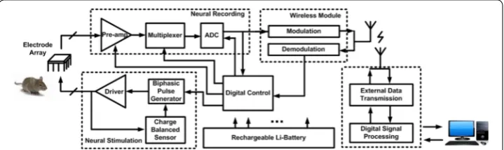
Figure 1 shows a block diagram of the neural interface that depict the recording and stimulation pathways. The stimulation path is used to deliver balanced charge into tis-sue, while the neural recording functions precondition the analog signals with amplify-ing, filtering and then analog-to-digital converting. Compared with the implementation of individual components, this integrated interface has the advantages of lower power, lower noise, smaller size, and higher precision.
permanent tissue damage. Passive charge balancing, active charge balancing and using the current source to remove residual charge have been previously described [15]. Power efficiency by energy recovery or recycling is also presented in many publications [14, 16,
8]. Although the design of Ref. [17] is power saving, the voltage-based stimulation has the disadvantage of a lack of control and the dynamic range is not wild.
Our objective with this proposed neural stimulator introduces calibration circuit and data flow to reduce charge imbalance to a least significant bit level caused by the effects of process variation and other non-ideal factors. Our design utilizes a high voltage pro-cess technology to allow for a wide output range needed for high impedance electrode technologies.
The remainder of this paper is organized as follows: “Methods” provides method, including system design, basic structure for neural stimulation, design specification, cir-cuit implementation and layout design of the neural stimulation. “Results” presents the result of the proposed neural stimulation. “Discussion” discusses the results and the per-formance of the system. “Conclusion” presents the conclusion of this paper.
Methods
This section will present an overview of the system design, the basic structure, the design specification and circuit implementation of the driver, calibration and the digital interface.
System design
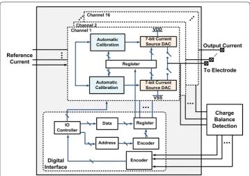
A block diagram of the 16-channel neural stimulator is shown in Fig. 2. Each channel comprises a 7-bit current driver, polarity switches, and a 10-bit d-latch register to store the calibrated current level per channel. To reduce the least-significant-bit (LSB) quan-tization error and the current mismatch, an automatic calibration flow diagram is pre-sented in this paper. The digital interface is used to control current driver switches and calibration switches all of the channels.
Basic structure for neural stimulation
There are several types of current mode stimulators. The single current mirror stack design approach is shown in Fig. 3a that depicts a positive currents source tied to VDD
and an negative currents source tied to VSS. Figure 3b shows a similar approach but with
dual current mirror stacks in the current driver [11, 12, 18, 19].
The power supply of the current driver shown in Fig. 3a, uses a bipolar power supply of VDD and VSS, which have the opposite and equal polarity thus providing both source
current and sink current respectively. The Ianodic and Icathodic currents are programmable
via the 7-bit register value to represent the anodic current and cathodic current, each of which are controlled by the switches S1 and S2. In Fig. 3b, there is a unipolar power
sup-ply of VDD and GND to current driver circuit. In one phase, S1 and S4 turn on, S2 and S3
turn off, and the charge is delivered from the left side to the right side of the electrode. In the following phase, S1 and S4 turn off, S2 and S3 turn on, and Isim flows from the right
side to the left side of the electrode.
Fig. 2 Block diagram of the system. The neural stimulator contains 16 channels. Each channel comprises a 7-bit current driver, polarity switches, calibration module and a register. The digital interface provides the control signal
The model of the biphasic current stimulator pulse and the typical electrode model are shown in Fig. 4, using both current source and sink [10, 14, 20]. An anodic pulse injects charge from the electrode into the neural tissue followed by an equal cathodic pulse with an opposite polarity charge in order to maintain the charge balance. TF is the train fre-quency, which is used to define the time period between each biphasic current pulse. TD is time duration, which represents how long the interval pulse will last.
Many researches have been proposed a variety of micro-electrodes models [21, 22]. The model of the electrode we used is found in the right side of the diagram in Fig. 4. This model electrode contains a parallel resistor Rf and capacitor Cdl with and a series
resistor, Rs. Rs is the solution spreading resistance and Cdl is the double-layer
capaci-tance, while Rf is the faradaic resistance [10]. Design specifications
The basic specifications of stimulator system must have several key characteristics including low power consumption, small physical size, long lifetime and reliability, high channel count of electrodes, and only a few external components [17]. For implantable neural stimulation, the procedure of implantation may cause mechanical damage. Small physical size will reduce tissue damage during implantation [15]. Once implanted, longer lifetime and higher reliability mean reducing the number of replacements, thereby reducing the possibility of damage during the implantation process and the user’s eco-nomic losses. Also we have more challenging requirements as constant current charge balance and high voltage range across a wide range of load impedances.
Neural stimulation is used to apply charge to neural tissue from the electrode [17]. The membrane potential of neurons is externally excited, and the neuron fires or action potential or spike as a response. Many factors, such as circuitry and frequency of stim-ulation, the shape of the waveform, and the location of the electrode, may affect the charge duration and transfer requirements of the stimulation pulses [23].
The impedance of the microelectrode is an important consideration. Many other elec-trode models are used with some form of conductance or a constant-phase element [8, 16,
17]. Each channel of the stimulator will drive high impedance electrodes load, which may vary in a wide range. The stimulation charge to neural tissue needs to be in the microam-pere to milliammicroam-pere current range. The current is equal to the voltage divided by the load resistance. Since the high-voltage process will charge the maximum stimulation current into high impedance electrodes, the high voltage process is applied in this paper.
Another important consideration is that of safety. Several methods have been cho-sen to achieve this goal. Because prolonged DC current and charge accumulation in the neural tissue causes permanent damage. The constant current driver needs to main-tain charge balance. To provide charge balanced stimulation, the accuracy and linearity of neural stimulation is important. In this paper, we propose an automatic calibration method to maintain an accurate charge balance output across the best case and worst case models of the complementary metal oxide semiconductor (CMOS) device manu-facturing process variations [24].
Circuit implementation
We developed a 16-channel biphasic current mode stimulator. Each unit consists of a 7-bit current Digital-to-Analog Converter (DAC), an automatic calibration module, and a digital control interface, which is shown in Fig. 5. The stimulator can be used in stimu-lation mode or calibration mode.
Current driver
The schematic of each channel is shown in Fig. 5. The 7-bit current DAC consists of the 7-bit binary-weighted current sink DAC and the current source DAC. The digital reg-ister controls the transmission gates to choose which branch is on. The sink and source currents are controlled by a polarity switch. Figure 6 shows the cathodic and anodic cur-rents of the current driver, according to the DAC code from 0 to 127. Both curcur-rents can be mirrored from 8 to 512 μA with a LSB current of 8 μA, so both current stimulations can be measured from 0 to 1016 μA.
Calibration
To maintain charge balance during electrical stimulation and reduce the effect of CMOS process variations, temperature, and the power supply, an automatic calibration tech-nique is proposed in this design. One main current and ten tuning currents form the current input to the DAC. The default setting is to turn five tuning currents on while the other five currents are off. When the anodic and cathodic currents are unequal, the cali-bration will start automatically.
When the stimulation mode is on, the calibration will be set as a default code and start to deliver charge. When the calibration mode is on, the voltage of the output node will be monitored by the off-chip analog-to-digital converter (ADC) and will send a signal back to the digital interface, which will send the control signal to the calibration register. A flow chart of the calibration process is shown in Fig. 7.
When the calibration starts, the maximum current is measured firstly. If the current has a negative imbalance, then the calibration register should be changed to increase the reference of the current source DAC or decrease the reference of the current sink DAC. If the current has a positive imbalance, then the reference of the current sink DAC should be increased or the reference of the current source DAC should be decreased. When the current is balanced, the calibration register stores the calibration data. A stable and charge-balanced current output can be achieved by adjusting the reference current.
Digital interface
The block diagram of the digital interface is shown in Fig. 2. Each channel of the stimula-tor drives high-impedance electrodes with individual channel controls for enable/dis-able, current, and phase. The current for each driver can be adjusted from 1 to 1016 μA using a 7-bit register. Because there are 16 channels, this register is 7 × 16 (112) bits wide. The current direction of each biphasic driver is controlled by another register.
The I/O controller controls the data and address paths. The data path is used to con-trol the switches of the current drivers and the calibration, while the address path is used to choose each channel. The I/O also controls the transmission gate of each channel to switch the anodic and cathodic currents.
Layout design
All individual circuit layouts for the constant current driver, calibration circuit layout and full chip layout was created to meet the design rules check (DRC) and layout versus schematic (LVS) rules of the 0.18 μm high voltage (HV) CMOS process technology using Mentor Graphics computer aided design (CAD) software.
The constant current driver layout was optimized to achieve the best device matching of the P-channel metal oxide semiconductor (PMOS) and N-channel metal oxide semicon-ductor (NMOS) devices using common centoid layout techniques. In addition, the mini-mum gate lengths of these devices were selected to be 2 or 3 times the minimini-mum gate length of 0.18 μm to minimize the effect of channel length modulation on small gate lengths.
As with the constant current driver layout previously mentioned above, we used com-mon centoid layout techniques of the calibration current mirrors to achieve the best device matching. Minimum gate lengths of these devices were also set to be 2 or 3 times the minimum gate length of 0.13 μm to minimize the effect of channel length modula-tion on small gate lengths.
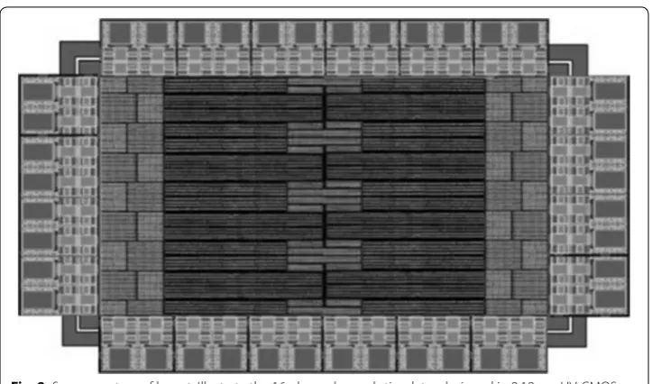
The full chip layout of the 16-channel stimulator chip was layout using 0.18 μm HV-CMOS technology, the layout and the printed circuit board (PCB) test board with a packaged application specific integrated circuit (ASIC) die is shown in Figs. 8 and 9, respectively. 16-channel stimulators are located common central. Guardring is applied to isolate noise and interference of each module. Electro-static discharge (ESD) protec-tion is used on I/O PAD.
Results
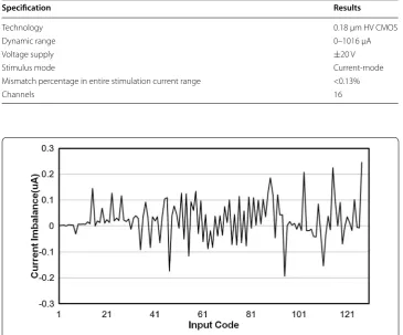
The power voltage supply was set to be ±20 V for tested as allowed by the HV-CMOS process specifications. The series load was varied from 1 to 20 KΩ to model the variation of stimulation electrode impedance of our simplified RC load model as shown in Fig. 4. Test results are summarized in Table 1.
The current pulse was calculated by measuring the voltage across the resistor load. Hence, the maximum amplitude of the biphasic current pulses was achieved at the maximum voltage output of ±20 V. The maximum anodic and cathodic currents were 1015.63 and 1015.87 μA, respectively, with an 8-μA step size of the 7-bit amplitude res-olution. Therefore, the current mismatch across the dynamic range of our output was below 0.3 μA.
Charge balancing performance is measured by calculating the difference between anodic and cathodic currents; the ideal difference is zero. Figure 10 shows the current
Fig. 8 Screen capture of layout. Illustrate the 16-channel neural stimulator designed in 0.18 μm HV-CMOS technology
imbalance as a function of the DAC input code, while Fig. 11 shows the imbalance per-centage as a function of the DAC input code. The worst current imbalance between anodic and cathodic current pulses occurred at the maximum stimulation current, while the imbalance percentage at the maximum stimulation current was less than 0.03%. Fig-ure 11 shows that over the entire stimulation current range, the charge delivery percent-age errors were less than 0.13%.
The current driver was tested across a wide range of load resistances. Figure 12 shows the voltage of the output node as the resistor load was varied from 1 to 10 KΩ. The four curves represent the output voltage of four different resister loads. As shown in Fig. 12, the current remained constant even when the load resistance and corresponding output voltage changed.
Discussion
We created a multi-channel biphasic constant current-mode neural stimulator with programmable current calibration. Each channel can operate in stimulation or calibra-tion mode to ensure a minimal current mismatch so charge balance is achieved across the manufacturing processes. A 7-bit current DAC was used for each stimulation chan-nel with small calibration current adjustments. Our stimulation system has a simpli-fied architecture compared with other constant current driver designs with calibration
Table 1 Performances of neural stimulation
Specification Results
Technology 0.18 μm HV CMOS
Dynamic range 0–1016 μA
Voltage supply ±20 V
Stimulus mode Current-mode
Mismatch percentage in entire stimulation current range <0.13%
Channels 16
in that we do not include any analog comparators or integrator circuits. Our approach simplifies the calibration result as a digital correction register value that is determined empirically and loaded during the calibration procedure, thus eliminating the need for any additional analog circuits as comparators and integrators.
We chose our constant current mode calibration stimulation approach for safety and precise control. Functional electrical stimulation is applied by injecting charge into neural tissue to detect the neural reaction [17]. There are two typical approaches for electrical stimulation. Voltage-based stimulation is designed to control the voltage between electrodes. This technique ensures higher energy efficiency, but it has the dis-advantage of a lack of control, especially when the tissue impedance varies significantly.
Fig. 11 Current imbalance percentage. Illustrate the relationship between imbalance percentage error and input DAC code of anodic current and cathodic current. The charge delivery percentage errors are within 0.13% over the stimulation range
Current-based stimulation directly controls the current between electrodes. Although current-based stimulation suffers from inefficiency and higher power consumption, it remains used for its safety and increased control, as the charge delivered to the tissue is directly proportional to the current [6, 8, 25]. There are other approaches, such as switched capacitor charge delivery [26].
Automatic calibration was introduced in this design to reduce charge imbalance, since charge balance is an important design consideration in neural applications for safety rea-sons. A mismatched biphasic pulse will accumulate extra charge and induce DC current flow, which will permanently damage neural tissue. In reality, it is difficult to generate a matched current because of the mismatch of MOS and process variations. The power supply and temperature changes will also significantly affect the stimulation current. We used a charge balanced sensor and a return control signal to the chip for automatic tuning. For a stimulation current of 1 mA, a current mismatch less than 0.3 μA was produced.
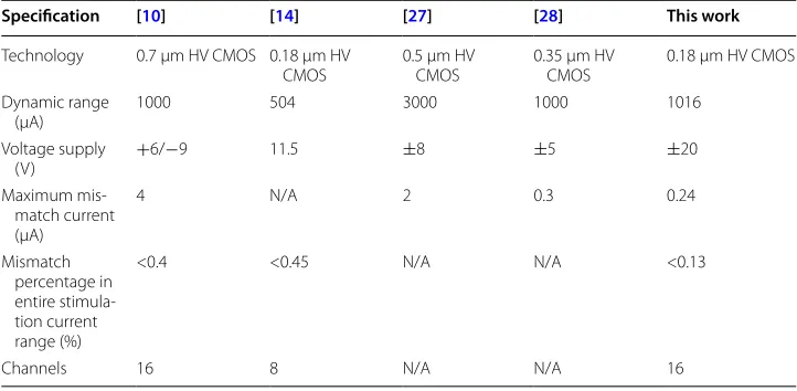
A 7-bit current DAC was used to provide a high tuning resolution. As shown in Table 2, our stimulator maintains a charge mismatch error below 0.13%. These other cal-ibration techniques [27–29] used on-chip integrators and comparators and redundant switches to reduce the anodic and cathodic charge mismatch. Our approach does not rely on any on-chip comparator or integrators since these components have inherent off-set and tolerance when placed on the chip.
Conclusion
This paper presents a 16-channel integrated biphasic current mode neural stimula-tor chip with calibration. The stimulastimula-tor circuit design was simulated and the chip layout was completed. The chip layout was verified using DRC and LVS design check using CAD software. Each channel can stimulate anodic and cathodic current, and the dynamic range reached 1 mA with 7-bit resolution. Calibration was used to minimize the current mismatch caused by the inherent CMOS manufacturing processes and other variations, and a charge imbalance below 0.13% was maintained. By designing the
Table 2 Comparison of the proposed neural stimulation
Specification [10] [14] [27] [28] This work
Technology 0.7 μm HV CMOS 0.18 μm HV
CMOS 0.5 μm HV CMOS 0.35 μm HV CMOS 0.18 μm HV CMOS Dynamic range
(μA) 1000 504 3000 1000 1016
Voltage supply
(V) +6/−9 11.5 ±8 ±5 ±20
Maximum mis-match current (μA)
4 N/A 2 0.3 0.24
Mismatch percentage in entire stimula-tion current range (%)
<0.4 <0.45 N/A N/A <0.13
stimulator ASIC with high-voltage CMOS technology, the electrode load impedances can vary significantly while maintaining constant current stimulation. The proposed multi-channel current-mode stimulator can keep the charge balanced and work safely.
Abbreviations
ADC: analog-to-digital converter; ASIC: application specific integrated circuit; CAD: computer aided design; CMOS: com-plementary metal oxide semiconductor; DAC: digital-to-analog converter; DRC: design rules check; HV: high voltage; I/O: input/output; LSB: least significant bit; LVS: layout versus schematic; NMOS: N-channel metal oxide semiconductor; PCB: printed circuit board; PMOS: P-channel metal oxide semiconductor.
Authors’ contributions
XL was responsible for the system design, circuits simulation, data analysis, and took the lead on manuscript writing and figures design. SZ performed the background review and system design. MJ supervised this research, performed the experimental design and revised the manuscript. All authors read and approved the final manuscript.
Acknowledgements
The authors gratefully acknowledge financial support from China Scholarship Council. We also gratefully acknowledge Triangle BioSystem International for technical support.
Competing interests
The authors declare that they have no competing interests. Availability of data and materials
All data generated or analyzed during this study are included in this published article (and its supplementary informa-tion files).
Consent for publication Not applicable.
Ethics approval and consent to participate Not applicable.
Funding
This work was supported by a grant from China Scholarship Council under Grant No. 201406030069.
Publisher’s Note
Springer Nature remains neutral with regard to jurisdictional claims in published maps and institutional affiliations. Received: 3 February 2017 Accepted: 22 July 2017
References
1. Hong Y, Lee HJ, Kim SG, et al. A label-free biosensing platform using a PLL circuit and Biotin-Streptavidin Binding system. IEEE Trans Biomed Circuits Syst. 2015;9(3):345–52.
2. Giagka V, Eder C, Donaldson N, et al. An implantable versatile electrode-driving ASIC for chronic epidural stimulation in rats. IEEE Trans Biomed Circuits Syst. 2015;9(3):387–400.
3. Valle YI, Parker AC. An astrocyte neuromorphic circuit that influences neuronal phase synchrony. IEEE Trans Biomed Circuits Syst. 2015;9(2):175–87.
4. Liu X, Zhang M, Subei B, et al. The PennBMBI: design of a general purpose wireless brain-machine-brain interface system. IEEE Trans Biomed Circuits Syst. 2015;9(2):248–58.
5. Roh T, Song K, Cho H, et al. A wearable neuro-feedback system with EEG—based mental status monitoring and transcranial electrical stimulation. IEEE Trans Biomed Circuits Syst. 2014;9(2):755–64.
6. Neustetter C, Zangerl M, Spitze P, et al. In-vitro characterization of a cochlear implant system for recording of evoked compound action potentials. Biomed Eng Online. 2012;11:22.
7. Kanchiku T, Suzuki H, Imajo Y, et al. The efficy of neuromuscular electrical stimulation with alternating currents in the kilohertz frequency to stimulate gait rhythm in rats following spinal cord injury. Biomed Eng Online. 2015;14:98. 8. Arfin SK, Sarpeshkar R. An energy-efficient, adiabatic electrode stimulator with inductive energy recycling and
feedback current regulation. IEEE Trans Biomed Circuits Syst. 2012;6(1):1–14.
9. Monge M, Raj M, Nazari MH, et al. A fully intraocular high-density self-calibrating epiretinal prosthesis. IEEE Trans Biomed Circuits Syst. 2013;7(6):747–60.
10. Sit JJ, Sarpeshkar R. A low-power blocking-capacitor-free charge-balanced electrode-stimulator chip with less than 6 na dc error for 1-ma full-scale stimulation. IEEE Trans Biomed Circuits Syst. 2007;1(3):172–83.
11. Chun H, Yang Y, Lehmann T. Safety ensuring retinal prosthesis with precise charge balance and low power con-sumption. IEEE Trans Biomed Circuits Syst. 2014;8(1):108–18.
• We accept pre-submission inquiries
• Our selector tool helps you to find the most relevant journal
• We provide round the clock customer support
• Convenient online submission
• Thorough peer review
• Inclusion in PubMed and all major indexing services
• Maximum visibility for your research
Submit your manuscript at www.biomedcentral.com/submit
Submit your next manuscript to BioMed Central
and we will help you at every step:
13. Sooksood K, Stieglitz T, Ortmanns M. An active approach for charge balancing in functional electrical stimulation. IEEE Trans Biomed Circuits Syst. 2010;4(3):162–70.
14. Williams I, Constandinou TG. An energy-efficient, dynamic voltage scaling neural stimulator for a proprioceptive prosthesis. IEEE Trans Biomed Circuits Syst. 2013;7(2):129–39.
15. Aryan NP, Kaim H, Rothermel A. Stimulation and recording electrodes for neural prostheses. Berlin: Springer; 2015. p. 17–22.
16. Kelly SK, Wyatt JL. A power-efficient neural tissue stimulator with energy recovery. IEEE Trans Biomed Circuits Syst. 2011;5(1):20–9.
17. Ortmanns M, Rocke A, Gehrke M, et al. A 232-channel epiretinal stimulator ASIC. IEEE J Solid State Circuits. 2007;42(12):2946–59.
18. Çilingiroğlu U, İpek S. A zero-voltage switching technique for minimizing the current-source power of implanted stimulators. IEEE Trans Biomed Circuits Syst. 2013;7(4):469–79.
19. Liu X, Demosthenous A, Donaldson N. An integrated implantable stimulator that is fail-safe without off-chip blocking-capacitors. IEEE Trans Biomed Circuits Syst. 2008;2(3):231–43.
20. Jiang D, Demosthenous A, Perkins TA, et al. A stimulator ASIC featuring versatile management for vestibular prosthe-ses. IEEE Trans Biomed Circuits Syst. 2011;5(2):147–59.
21. Waschkowski F, Hesse S, Rieck AC, et al. Development of very large electrode arrays for epiretinal stimulation (VLARS). Biomed Eng Online. 2014;13:11.
22. Yang F, Yang CH, Wang FM, et al. A high–density microelectrode–tissue–microelectrode sandwich platform for application of retinal circuit study. Biomed Eng Online. 2012;11:33.
23. Merrill DR, Bikson M, Jefferys JGR. Electrical stimulation of excitable tissue: design of efficacious and safe protocols. J Neurosci Meth. 2005;141:171–98.
24. Shulyzki RS, Abdelhalim K, Bagheri A, et al. 320-Channel active probe for high-resolution neuromonitoring and responsive neurostimulation. IEEE Trans Biomed Circuits Syst. 2015;9(1):34–49.
25. Abdelhalim K, Jafari HM, Kokarovtseva L, et al. 64-Channel UWB wireless neural vector analyzer SOC with a closed-loop phase synchrony-triggered neurostimulator. IEEE J Solid State Circuits. 2013;48(10):2494–510.
26. Ghovanloo M. Switched-capacitor based implantable low-power wireless microstimulating systems. In: IEEE ISSCC Digest of Technical Papers, 2006: 2197–2200.
27. Lee EK, Lam A. A matching technique for biphasic stimulation pulse. IEEE Int Symp Circuits Syst. 2007;2007:817–20. 28. Guo S, Lee H. Biphasic-current-pulse self-calibration techniques for monopolar current stimulation. IEEE Int Symp
Circuits Syst. 2009;2009:61–4.