Volume 2, Issue 3, 2015
70
Available online at www.ijiere.com
International Journal of Innovative and Emerging
Research in Engineering
e-ISSN: 2394 - 3343 p-ISSN: 2394 - 5494
Diamond Chips
Kaushtubh Jha
a, Devesh Sapkale
aand Pravin Ahirwar
aa, Student, Department of Computer Science & Engineering,
Shri Sant Gadge Baba College of Engineering & Technology, Near Z.T.C.,
Bhusawal - 425203, Maharashtra, India
ABSTRACT:
The main objective is to appraisal mounting technology “Diamond Chip” also recognized as Carbon Chip. Electronics without silicon is implausible, but it will come true with the evolution of Diamond or Carbon chip. Manufacturing using Electronic Chips has numerous drawbacks when it is used in electronic applications, due to bulk in size, slow operating speed etc. Industrialists plan to build a diamond chip that can resist in temperatures of 500 C, associated to only about 150 C for silicon chips.
Keywords: Carbon Nanotubes (CNT), Single Walled Nanotubes (SNWT), Multi Walled Nanotubes.
I. INTRODUCTION
Currently we are using silicon for the manufacturing of Electronic Chip’s. It has many drawbacks when it is used in power electronic applications, such as majority in size, slow working alacrity etc. Carbon, Silicon and Germanium are belonging to the similar cluster in the episodic table. A crystalline diamond film that could fabricate more resilient semiconductor chips than those made from silicon, generally synthetic diamonds have proved a poor semi conduct material Diamond can also stand firm voltages up to around 200 volts, compare to around 20 volts for a silicon chip.
.
II. CARBONNANOTUBES(CNT)
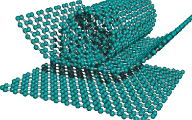
Downfall the Graphene sheet into a tube like structure produces CARBON NANOTUBES. It is a Nano size cylinder of carbon atoms. They are through of one or a number of concentric walls in which carbon atoms are prearranged in hexagonal pattern, having a less than one nanometer diameter [2].
Figure 1: Carbon Nanotubes (CNT)
III. PRODUCTIONMETHODSOFCARBONNANOTUBE
There are various production methods. Three main methods are:
A. ARC DUSCHARGE METHOD
The arc-plasma disappearance of untainted graphite rods led to the innovation of CNT by Iijima. The arc device used was the alike as that for the invention of ultrafine SiC particles by a gas evaporation process. CNTs were obtained in the cathode deposit prepared by a dc arc discharge method in rarefied His gas. This arc evaporation of carbon electrodes produced a set down on the cathode, which incorporated multiwall carbon nanotubes (MWNTs) [1].
B. PULSED LASER EVAPORATION
Volume 2, Issue 3, 2015
71 conducted in a predictable vacuum chamber operational with a window of high transmittance for the wavelength of the pulsed laser to be used. Authentication proceeds by illuminating the target with laser pulses. To make the MAPLE target, 1.1 gm. of polymer, either polystyrene (PS) or polyethylene glycol (PEG), is mixed with 25 gm. of solution [3]. Because the ratio of SWN to chloroform cannot be determined, the exact ratio of SWN/polymer in the target is not known.
C. SILICON CARBIDE VAPORISATION
Associated CNT’s are fashioned on the surface of silicon carbide (SiC) wafers during high hotness anneals. The exposed 4H SiC surface transforms into CNT’s for temperatures in the range of 1400-1700°C and beneath moderate vacuum conditions. The carbon source is believed to be outstanding carbon from the SiC left on the surface after preferential disappearance of Si. CNT development is believed to be catalyzed by low concentrations of residual oxygen in the chamber [2].Patterning of both n-type and semi-insulating substrates with Si3N4 masks, former to annealing, results in CNT-free regions.
Vertically make parallel carbon nanotubes are much loved for applications in vacuum microelectronics as countryside emission diplomacy. A catalyst-free CNT augmentation means dubbed “surface decomposition” results from heating silicon carbide (SiC) wafers in a vacuum furnace.
IV. TYPESOFCARBONNANOTUBES(CNT)
There are two types of carbon nanotubes:
A. SINGLE WALLED NANOTUBES (SNWT)
Single Walled Nanotube is a nanotube, which has merely one graphite layer. It is tacit that one graphite layer is in use and it is fold in a cylindrical silhouette to formulate a CNT. SNWT is semiconductor, which exhibit band gap energy of 0.3 eV. Current transmission takes place from side to side the walls. As the diameter augment the band gap energy decreases and it show evidence of metallic properties [5].
Figure 2: Single Walled Nanotubes (SNWT)
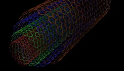
B. MULTI WALLED NANOTUBES (MWNT)
Multi walled carbon nanotube is a nanotube which has manifold layer state line. It is unspecified that a deposit of graphite layers is in use and which is folded cylindrical shape to make the MWNT. Multi walled carbon nanotubes are mostly clanging in nature. The energy band gap is in the order of zero [4].The diameter of multi walled carbon nanotube is superiorto that of single walled carbon nanotube. It is not second-hand for the manufacturing of semiconductor devices like CNT transistor since it will not give a ‘cut off’ on the application of the gate voltage.
Figure 3: Multi Walled Nanotubes (MWNT)
V. PROPERTIESOFCARBONNANOTUBE
A. STRENGTH
Volume 2, Issue 3, 2015
72 Figure 4: Strength
B. HARDNESS
Customary single walled carbon nanotubes can endure heaviness up to 24GPa without buckle. They then experience a transformation to super hard segment nanotubes. Maximum pressures measured using current untried techniques are around 55GPa [1].
The bulk modulus of super hard stage nanotubes is 462 to 546 GPa, even senior than that of diamond (420 GPa for single diamond crystal).
Figure 5: Hardness
C. ELECTRICAL
High electrical conductivity (10-6 ohm), and for well crystallized nanotubes ballistic transport is observed. Being covalently
bonded, as electrical conductors they do not suffer from electro migration or atomic diffusion and thus can carry high current densities (107 -109 A/cm2), which is 1000 times that of copper. In cooperation metal and semiconductor can be
formed [3].
Figure 6: Electrical
D. THERMAL
Volume 2, Issue 3, 2015
73 Figure 7: Thermal
VI. ADVANTAGESOFCARBONNANOTUBES(CNT)
A. AVERAGE DIAMETER
The Japanese Scientist finished the minimum CNT, the diameter of that carbon nanotube is just 0.4nm.The run of the mill diameter of the carbon nanotube is 1.2 nm to 1.4nm.The diameter vary according to the industrialized process. E-beam lithography can produce lines of 50 nm wide.
B. GOOD THERMAL
The thermal conductivity of the carbon nanotube is 6000 w/m/k so the heat debauchery in the circuitry is quickly passed to the high temperature sink or other cooling instrument. On assessment pure diamond will broadcast heat at the rate of 3320 w/m/k.
C. HIGH TENSILE STRENGTH
Carbon nanotube has a tensile strength of 45 billion Pascal. Where as a high strength steel alloy break at about 2 billion Pascal .So NASA is planning to use carbon nanotube for spacecraft component manufacturing.
D. HIGH DENSITY
Carbon nanotube has very elevated density of 1.33 to 1.40 grams per Cm Square. So NASA is planning to use CNT alloys in the nozzles of future space shuttles.
E. TWISTING ANGLE
Carbon nanotube has an important property called twisting angle dependence. Run of the mill MWNT show evidence of clanging character. But it is conditional on its falsification angle. The band gap of the carbon nanotube increases with its twisting angle .So this method can be used to convert metallic carbon nanotubes in to semi conducting CNT. Atomic force microscope is used to make twist in the carbon nanotube .It is operated in contact mode to make these twist [5].
F. HIGH MOBILITY
Mobility of the electrons inside the doped diamond structural carbon is higher than that of in the silicon structure. As the size of the silicon is higher than that of carbon, the chance of collision of electrons, with larger silicon atoms increases as compared to carbon chip.
VII. HOWNANOTUBESAREUSEFULINDIGITALLOGIC?
Their straightforward inverter machine consists of a nanotube FET and a large bias confrontation. It converts a elevated input voltage to a low one - that is, "one" to "zero" - and vice versa. By adding up an extra FET in parallel, the researchers made a NOR gate [4]. This device needs two "zero" inputs to give a "one" output, or two "ones" to give a "zero”. Any of the typical logic gates - AND, OR, NAND and so on - can be shaped using dissimilar arrangements of these FETs.
A. ADVANTAGES OF DIAMOND CHIP
1. SMALLER COMPONENTS ARE POSSIBLE
As the dimension of the carbon atom is little compared with that of silicon atom, it is probable to etch very lesser lines through diamond structural carbon. We can become conscious a transistor whose size is one in hundredth of silicon transistor.
2. IT WORKS AT HIGHER TEMPERATURE
Volume 2, Issue 3, 2015
74 these eminent high temperatures. Diamond is very good conductor of heat. So if there is any heat indulgence inside the chip, heat will very quickly transport to the heat sink or other cooling technicalities.
3. FASTER THAN SILICON CHIP
Carbon chip works previous than silicon chip. The mobility of the electrons within the doped diamond structural carbon is higher than that of in the silicon organization. As the size of the silicon is highly developed than that of carbon, the chance of impact of electrons with larger silicon atoms increases [2]. Except the carbon atom size is small, so the opening of impact decreases. So the mobility of the charge carriers is elevated in doped diamond structural carbon compare with that of silicon.
4. LARGER POWER HANDLING CAPACITY
It has many drawbacks such as bulk in size, slow operating speed, smaller amount efficiency, lower band gap etc. At very high voltages silicon structure will collapse. It is unspecified that a carbon transistor will distribute one watt of power at speed of 100 GHZ. Now days in all power electronic circuits, we are by means of certain circuits like relays, or MOSFET inter connection circuits (inverter circuits) for the purpose of interconnecting a low power control circuit with a high power circuit [3].If we are using carbon chip this inter stage is not desirable. We can connect high power circuit direct to the diamond chip.
VIII. CONCLUTION
Carbon is more appreciated than Silicon. By means of carbon as the manufacturing material, we can accomplish smaller, faster and stronger chips. Therefore diamond chip substitutes the need of silicon in every aspect in future generation and we can get fast, small electronic devices.
ACKNOWLEDGMENT
We would like to thank our honorable Principal, Dr. R. P. Singh, our Head of Department, Prof. D. D. Patil , & our special thanks to our guide, Prof. R. P. Chaudhari and & sincere thanks to all the respected teaching faculties of department of computer science & engineering. Our special thanks to all the writers of reference paper that are referred by us.
REFERENCES
[1] http://www.infoworld.com/t/platforms/study-carbon-nanotubes-make-best semiconductors-487.
[2] Diamond Science and Technology, volume 1 Aleksandra Mikhailovich Prokhorov Technology and Engineering (2002).
[3] Jorg D (2002). Hoheisel technology And Engineering.
[4] C.-F. Chen, C.-L. Lin, and C.-M. Wang, “Field emission from aligned carbon nanofibers grown in situ by hot filament chemical vapor deposition,” Appl. Phys. Lett. 82, 2515 (2003).