© Copernicus GmbH 2004
Advances in
Radio Science
Generation of short electrical pulses based on bipolar transistors
M. Gerding, T. Musch, and B. Schiek
RF and Microwave Institute, Ruhr-Universitaet Bochum, Universitaetsstrasse 150, 44780 Bochum, Germany
Abstract. A system for the generation of short electrical pulses based on the minority carrier charge storage and the step recovery effect of bipolar transistors is presented.
Electrical pulses of about 90 ps up to 800 ps duration are generated with a maximum amplitude of approximately 7 V at 50. The bipolar transistor is driven into saturation and the base-collector and base-emitter junctions become for-ward biased. The resulting fast switch-off edge of the transis-tor’s output signal is the basis for the pulse generation. The fast switching of the transistor occurs as a result of the mi-nority carriers that have been injected and stored across the base-collector junction under forward bias conditions. If the saturated transistor is suddenly reverse biased the pn-junction will appear as a low impedance until the stored charge is de-pleted. Then the impedance will suddenly increase to its nor-mal high value and the flow of current through the junction will turn to zero, abruptly.
A differentiation of the output signal of the transistor re-sults in two short pulses with opposite polarities. The differ-entiating circuit is implemented by a transmission line net-work, which mainly acts as a high pass filter.
Both the transistor technology (pnp or npn) and the phase of the transfer function of the differentating circuit influence the polarity of the output pulses. The pulse duration depends on the transistor parameters as well as on the transfer func-tion of the pulse shaping network.
This way of generating short electrical pulses is a new al-ternative for conventional comb generators based on step-recovery diodes (SRD). Due to the three-terminal structure of the transistor the isolation problem between the input and the output signal of the transistor network is drastically sim-plified. Furthermore the transistor is an active element in contrast to a SRD, so that its current gain can be used to min-imize the power of the driving signal.
Correspondence to: M. Gerding
1 Introduction
The use of rf-transistors as key components in comb gener-ators provides a new, more comfortable and more cost ef-fective way of generating short electrical pulses as compared to step-recovery diodes (HP, 1988). The achievable pulse length, the output power and pulse polarity can be influenced by the choice of the rf-transistor, the rf-transistor technol-ogy and the dimensions of the pulse shaping network. The transistor based circuit offers a wide range of different con-figurations so that its properties can be adapted to the field of applications relatively easily. The employed bipolar transis-tors are standard rf-components. This provides a good avail-ability and a wide spectrum of different electronic specifica-tions. The current gain of the transistor and its three terminal character are further advantages compared to a passive step-recovery diode. Because of this, low power input signals lead to an output peak pulse power of nearly 1 W, e.g. 7 V at 50. The pulse duration can be adjusted between 90 ps and 800 ps.
2 Functional principle
The two comb generators shown in Fig. 1 consist of a driver circuit, a slope accelerator or speed-up stage with a npn- or pnp-bipolar transistor and a pulse shaping network.
pnp-transistor npn-transistor
dt t dU()
dt t dU() t
t t
t
pnp-transistor npn-transistor
dt t dU()
dt t dU() t
t t
t
Fig. 1. Functional principle of the transistor based comb generator.
of the trigger signal, the base-emitter and the base-collector diode become forward biased: the transistor is in the satura-tion mode. The trailing edge of the trigger signal causes a fast depletion of the stored charge in the base-collector junc-tion which leads to a sudden increase of the base-collector impedance. This causes an abrupt change of the voltage across the collector-emitter junction. Compared to the trail-ing edge of the input signal, the rise time at the output is shorter by a factor of approximately 10. By using fast logic gates for the driving stage of the speed up network, a result-ing rise time of less than 100 ps can be achieved at the output of the transistor. The polarity of the fast switch-off edge can be influenced by the choice of the transistor technology and by the transistor circuit. The signals shown in Fig. 1 belong to a common emitter circuit. Because of its current gain the common emitter circuit proves to be very suitable for this ap-plication. The next element in the signal path is the so called pulse shaping network behind the transistor network. This circuit by itself can be divided into two parts. The first one, the differentiating network forms a pulse from the switch-off edge of the output signal of the transistor. A simple differ-entiation of the rectangular output signal leads to a signal, which shows two pulses with different pulse polarities and differently sharp pulses. Not only the fast trailing edge of the signal is being differentiated, the slower leading edge is dif-ferentiated, too. The comparably slow leading edge results in a low pulse amplitude, which has to be suppressed e.g. by a clipping network which can be based on a passive diode net-work or an active transistor netnet-work. Then the output signal of the comb generator will ideally contain a sharp and short pulse.
3 Configuration of the comb generator
As mentioned above, the comb generator consists of three different stages. Two of these are explained in detail in the following chapters.
3.1 The speed-up network
The speed-up network mainly consists of a transistor circuit. Although common base, common emitter or common collec-tor circuits are all usable for this operation, this work is con-centrated on the common emitter circuit, which is the most
0 1 2 3 4 5 6
−30 −20 −10 0 10 20
Broadband amplifier based on a BFP520 (Infineon), npn−transistor
f/GHz
dB
|S21|
|S 22|
|S
11|
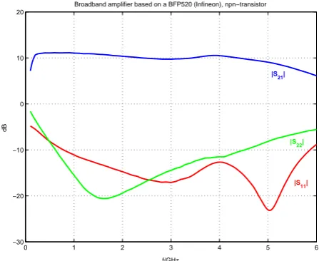
Fig. 2. Simulated Scattering parameters of a broadband amplifier
based on a npn rf-transistor (BFP520, Infineon).
useful circuit for this application, because of its high current gain.
Short pulses with a pulse duration of about 100 ps result in a broadband spectrum with a high corner frequency of sev-eral GHz. In a first step the transistor can be seen as a broad-band amplifier realized as an emitter circuit. Therefore, the linear transient response of the transistor circuit is optimized for a flat gain of about +10 dB and a flat frequency range up to 6 GHz. Figure 2 shows the simulated scattering parameters of the transistor circuit. Among others, the bandwidth of the amplifier depends on the specifications of the rf-transistor. As a rule of thumb, the faster the transistor, the shorter the switch-off edge.
As mentioned above, the transistor has to be driven into saturation, to get the fast step-recovery effect. Figure 3 shows a measurement of the input- and the output signal of a npn-transistor in a common emitter circuit. As expected, the out-put signal (red line) is inverted, as caused by the common emitter circuit. Figure 3 gives a comparison of the falling edge of the input signal (blue line) and the corresponding rising edge of the output signal (red line).
3.2 Differentiation network
0 2 4 6 8 10 12 14 16 18 20 −3
−2.5 −2 −1.5 −1 −0.5 0 0.5 1 1.5 2
t/ns
U/V
Input signal
Output signal
Fig. 3. Measurement of the input- and output signal of the speed-up
network.
3.2.1 Shorted branch line network
Figure 4 shows the simplest realization of a planar differen-tiating network. The high-pass character which is shown as a simulation result in Fig. 4, is achieved by the branch line shorted to signal ground. Both, the width and the length of the branch line influence the pulse shape. The length of the line shifts the corner frequency of the transfer function and the width determines the line impedance. It is a disadvantage that there is no complementary structure to shift the phase of the input signal by 180◦in order to achieve a pulse inversion. The only way to get different pulse polarities by this structure is to use different transistor technologies, i.e. pnp-transistors instead of npn-transistors
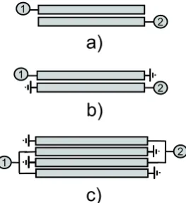
3.2.2 Coupled-line coupler as differentiating network The use of planar coupled-line structures solves the problem of the pulse inversion. The magnitude of the transfer func-tion of the coupled-line structure is nearly equivalent to the shorted branch line structure mentioned above. In fact the coupled-line structure has two more parameters which have to be optimized. Aside from the length and the width of each line, the two additional parameters are the coupling between the lines and the termination of each line. As it is shown in Fig. 5 the lines can be left open or can be shorted to ground at their ends. It can be shown theoretically by the use of coupled-line equivalents and the Kuroda identities, that the different terminations result in a phase shifting of the input signal (Malherbe, 1979). The theoretical phase difference between the transfer function of both structures is 180◦at the quarter wavelength frequency and nearly 180◦ over a wide frequency range. Because of this, the coupled-line structure with shorted lines changes the polarity of the output signal. When realizing these structures, the coupling between the two lines is critical. To maximize the coupling and to mini-mize the transmission loss, the coupling has to be tight. This means that the distance between the two lines has to be as
1 2
1 2
Fig. 4. Simulated transfer function of the shorted branch line
net-work, optimized for relatively slow pulses.
1
2
1
2
1
2
a)
b)
c)
Fig. 5. Coupled-line differentiating network: (a) not inverting, (b)
and (c) inverting.
narrow as possible, e.g. 75µm or 100µm. To overcome this mechanical limitation, two or more coupled-line structures can be combined in parallel.
Figure 6 illustrates the simulated results of the differential phase between the two alternative circuits (open end, shorted end). As expected, the difference is about 180◦over a wide
frequency range.
3.2.3 Transformer based differentiating network
Instead of the planar structures, transformers can be used as differentiating networks. Their function is comparable to the coupled-line structures. This means, coupling, input and out-put impedance and the possibility of changing the pulse po-larity are adjustable parameters. As it is illustrated in Fig. 7, the direction of winding influences the signal inversion.
0 6 f / GHz
-200 -100 0 100 200 P h a s e (S 2 1 ) / ° 2.735 GHz -103.6 ° 2.729 GHz 80.6 ° structure structure 6 f / GHz
-200 -100 0 100 200 P h a s e (S 2 1 ) / ° 2.735 GHz -103.6 ° 2.729 GHz 80.6 °
2 4 6
f / GHz -200 -100 0 100 200 P h a s e (S 2 1 ) / ° 2.735 GHz -103.6 ° 2.729 GHz 80.6 ° structure b) structure a) 6 -50 -40 -30 -20 -10 0 |S 2 1 | / d B
f / GHz
structure a)
structure b)
0 2 4 6
-50 -40 -30 -20 -10 0 |S 2 1 | / d B
f / GHz
structure a)
structure b)
Fig. 6. Simulated phase and magnitude of the transfer function of different coupled-line structures (see Fig. 5), open end (a), shorted end (b).
not inverting inverting
1 2 1 2
not inverting inverting
1 2 1 2
Fig. 7. Functional principle of transformer based differentiating networks (inverting, not inverting).
3.3 Function of the clipping network
The second stage of the pulse shaping network consists of the so called clipping network. Although there are several possible realisations of clipping networks, this contribution focuses on a passive, relatively simple and robust method. A fast Schottky diode is connected in series with the output of the differentiating stage. Depending on the diode’s polarity, the negative or the positive part of the input signal is clipped. Figure 8 illustrates this functionality. The left diagram shows the output signal of the differentiating stage at the in-put of the clipping network. The slow negative pulse,which is a result of the differentiation of the slow leading edge of the output signal of the transistor network, should be cancelled by the clipping network. The right diagram in Fig. 8 shows the output signal of the clipping network. The slow negative pulse is nearly completely eliminated as desired. The small residual signal is caused by a capacitive coupling which can mainly be explained by the junction capacitance and the par-asitic capacitance of the diode. The smaller the parpar-asitic ca-pacitance the smaller the coupled rest of the signal. Further-more, the diode should have a very low forward resistance to minimize the forward voltage drop across the diode.
4 Results of exemplary measurements
4.1 Comparison of different pulse polarities
Figure 9 gives an overview of different pulse shapes with different polarities and pulse durations. As mentioned above, the pulse polarity can be determined by the choice of the tran-sistor technology (npn or pnp) and by the proper realization of the pulse shaping network. The left diagram shows two traces measured with two identical pulse generator circuits both with a shorted branch line as a differentiating network. They only differ in the transistor used. Comparing both out-put signals, the negative pulse is longer than the positive one by a factor of 1.5. Taking the transient frequency of a tran-sistor as criteria, npn-trantran-sistors are generally faster, which results in shorter rise times of the switch-off edge and thus in shorter pulses.
BFP540 without clipping diode
BFP540, Schottky diode C=1.5pF
tPulse=180ps tPulse=150ps
1ns/div 1V/div
1ns/div 1V/div 1ns/div1ns/div 1V/div1V/div
Fig. 8. Measured input and output signal of the clipping stage, left: input signal, right: output signal based on a standard Schottky diode as
the clipping element.
open end lines shorted lines BFR194
BFR183 tPulse=237ps
tPulse=343ps
tPulse=190ps
tPulse=153ps
500ps/div 1V/div
500ps/div 1V/div
500ps/div 1V/div
500ps/div 1V/div
Fig. 9. Left: different pulse polarities caused by different transistor technologies (npn and pnp), right: changing the pulse polarity by different
coupled line structures.
5 Conclusion
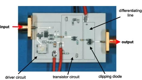
A robust comb generator based on fast rf-transistors has been presented. The complexity of the circuit design shown in Fig. 10 is relatively low, and since it uses standard compo-nents it is also quite cost effective.
The main characteristics are the flexibility in choosing the pulse length, the pulse amplitude and the choice of the pulse polarity. Each of the two complementary structures, one based on a npn-transistor, the other on a pnp-transistor, can be modified by the use of various differentiating networks to modify the pulse shape in detail. The maximum output peak pulse power is about 1 W with 7 V at 50and a pulse duration between 90 ps up to 800 ps can be obtained. This results in baseband signals with a high harmonic content up to 10 GHz.
Fields of application for such comb generators are for ex-ample the time domain reflectometry, distance to fault mea-surements on transmission-lines and level gauging measure-ments.
driver circuit transistor circuit
differentiating line
clipping diode input
output
driver circuit transistor circuit
differentiating line
clipping diode input
output
Fig. 10. Pulse generator circuit with shorted branch line and
References
Hewlett Packard: Application Notes AN918, Pulse and Waveform Generation with Step Recovery Diodes.
Hewlett Packard: Application Notes AN920, Step Recovery
Diodes, 1988.
Hoffmann, K.: Modelle und Schaltungen, Oldenbourg, 3. Auflage, 1996.
Malherbe, J. A. G.: Microwave Transmission Line Filters, Artech House, 1979.
Matsumoto, A.: Microwave Filters and Circuits, Academic Press, 1970.
Paul, R.: Transistoren, Vieweg, 1965.
Schiek, B.: Grundlagen der Hochfrequenz-Messtechnik, Springer Verlag, 1999.
Schrenk, H.: Bipolare Transistoren, Springer Verlag, 1978. Smith, P. W.: Transient Electronics, Wiley & Sons Ltd, 2002. Tietze, U. and Schenk, Ch.: Halbleiter Schaltungstechnik, 10.