Organized by C.O.E.T, Akola. Available Online at www.ijpret.com28
INTERNATIONAL JOURNAL OF PURE AND
APPLIED RESEARCH IN ENGINEERING AND
TECHNOLOGY
A PATH FOR HORIZING YOUR INNOVATIVE WORK
DEVELOPMENT OF SOLID OXIDE FUEL CELLS (
SOFC
) and ELECTROLYZERS
FOR FUTURE’S RENEWABLE ENERGY
DR. DHARMENDRA C. KOTHARI1, PROF. GANPAT B. SURALKAR R2
1. Department of Chemical Engineering & Technology, College of Engineering & Technology, Babhulgaon (Jh), Akola 444 104, (M.S).
2. Department of Chemistry (Chemical Science), College of Engineering & Technology, Babhulgaon (Jh), Akola 444 104, (M.S).
Accepted Date: 12/03/2016; Published Date: 02/04/2016
Abstract:Among the several ways of collecting solar energy, the photovoltaic, the photochemical, the photo-electro-chemical, the photo thermal and the photosynthetic are some of the better known routes to achieve energy conversion. Out of all these ideas of converting solar energy directly into the chemical energy or electrical energy by use of photo-electro-chemical systems has rapidly gained popularity in recent years. In the present paper, crystal structures of perovskite-type compounds such as CH3NH3PbI3, CH3NH3PbCl3,
CH3NH3PbBr3, CsSnI3, CH3NH3GeCl3, and CH3NH3SnCl3, are expected for solar cell materials, are reviewed and summarized. Since these
perovskite-type materials often have nanostructures in the solar cell devices, summarized information on the crystal structures would be useful for structure analysis on the perovskite-type crystals. Proton and oxide ion conducting perovskites are important in the development of solid oxide fuel cells (SOFC) and electrolysers (SOEC), gas separation membranes, sensors, etc. Perovskites are materials which allow considerable amount of suitable substitution in the cationic or anionic site so that their properties can be altered significantly. Importantly transmission electron microscopy, (TEM) studies reveal that the cation, arrangements in the different crystal structures established by different perovskites are either similar or closely related.
Keywords: Perovskite, SOFC, SOEC, Solar Cells, TEM, & PCE.
Corresponding Author: DR. DHARMENDRA C. KOTHARI
Co Author: PROF. GANPAT B. SURALKAR R
Access Online On:
www.ijpret.com
How to Cite This Article:
Dharmendra C. Kothari, IJPRET, 2016; Volume 4 (8): 28-40
PAPER-QR CODE
SPECIAL ISSUE FOR
NATIONAL LEVEL CONFERENCE
"RENEWABLE ENERGY
Organized by C.O.E.T, Akola. Available Online at www.ijpret.com29
INTRODUCTION
India is endowed with abundant of solar radiation. The country receives solar radiation equivalent to more than 5,000 trillion kWh/year, which is far more than its total annual energy requirement. The radiation available could be utilized for thermal as well as for photovoltaic applications. Solar thermal technologies have already found ready acceptance for a variety of decentralized applications in domestic, industrial and commercial sectors of the country. The most widely acceptable application is the solar water heating technology.
Figure (1):- ABX3 perovskite structure showing BX6 octahedral and larger A cation occupied in
cubo-octahedral site and Unit cell of cubic CH3NH3PbI3 perovskite, [1].
In perovskite structures with the general formula of ABX3 (X = oxygen, carbon, nitrogen or
halogen), A cation is occupied in a cubo-octahedral site and B cation is occupied in an octahedral site, Figure (1). When O2− anion is used, A and B are usually divalent and tetravalent,
respectively. However, perovskite containing halogen anions allow mono-valent and divalent cations in A and B sites, respectively, to fulfill charge neutrality. The formability of perovskite is estimated based on its geometric tolerance factor (t), t = (rA + rX)/[√2(rB + rX)], where rA, rB and
rX are the effective ionic radii for A, B and X ions, respectively. For transition metal cations
containing oxide perovskite, an ideal cubic perovskite is expected when t = 1 while octahedral distortion is expected when t < 1. Symmetry also decreases for t < 1, which may affect electronic properties. For alkali metal halide perovskite, formability is expected for 0.813 < t < 1.107.
Perovskite, named after a Russian mineralogist Lev-Perovski, is cubic ABX3 material consisting of
corner-sharing octahedral (BX6) with the A-cation occupying a 12-fold coordination site (Figure 1). In CH3NH3PbI3 perovskite, A is a mono valent cation CH3NH3 +, B is a divalent cation Pb2+,
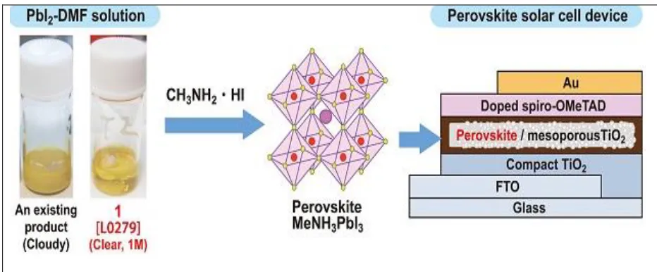
Organized by C.O.E.T, Akola. Available Online at www.ijpret.com30 solution of PbCl2 and CH3NH3I in DMF is prepared, [2]. This molar ratio reflects the ratio for lead
and iodide (1:3) in the final material, that is, CH3NH3PbI3. The PbCl2 and CH3NH3I are both white
powders, indicating wideband - gap materials. Interestingly, after mixing the two in DMF, the resulting solution is yellow, which is attributed to the formation of PbIx clusters in solution (note that PbI2 powder is yellow). Regarding the stability of the final material, it is interesting to
note that grinding the PbI2 and CH3NH3I powders directly without a solvent, also forms black
perovskite powder, indicating its stability over individual components.
Perovskite solar cells based on organometal halides represent an emerging photovoltaic technology. Perovskite solar cells stem from sensitized solar cells. In a liquid-based dye-sensitized solar cell structure, the adsorption of methyl ammonium lead halide perovskite on a nanocrystalline TiO2 surface produces a photocurrent with a power conversion efficiency (PCE)
of around 3–4%, as first discovered in 2009. The PCE was doubled after 2 years by optimizing the perovskite coating conditions. However, the liquid-based perovskite solar cell receives little attention because of its stability issues, including instant dissolution of the perovskite in a liquid electrolyte. A long term, stable, and high efficiency (~10%) perovskite solar cell was developed in 2012 by substituting the solid hole conductor with a liquid electrolyte. Efficiencies have quickly risen to 18% in just 2 years. Since PCE values over 20% are realistically anticipated with the use of cheap organometal halide perovskite materials, perovskite solar cells are a promising photovoltaic technology, [3].
LITERATURE
Recently, organic-inorganic hybrid solar cells with perovskite-type pigments have been widely fabricated and rapidly studied, [4 & 5]. Solar cells with a perovskite structure have high
conversion efficiencies and stability as the organic solar cells. Since a photo conversion efficiency of 15% was achieved [9], higher efficiencies have been reported for various device
structures and processes [10], and the photoconversion efficiency was increased up to 19.3% [11 & 12]. The photovoltaic properties of solar cells are strongly dependent on the fabrication process,
Organized by C.O.E.T, Akola. Available Online at www.ijpret.com31
Progress in Solar Cell Efficiency.
Sungkyunkwan University (SKKU), Korea Research Institute of Chemical Technology, (KRICT) and École polytechnique fédérale de Lausanne, (EPFL).
Wakamiya et al. reported that use of highly purified lead(II) iodide is a key to fabricate efficient perovskite solar cell devices (PCE > 10%) with high reproducibility.
Figure (2):- Development of Solid-state perovskite solar cells.
At first, perovskite light absorbers were used as sensitizers in liquid dye-sensitized solar cells. Perovskite can be dissolved in polar solvent because of its ionic solid nature, which limits further development of perovskite-sensitized photoelectron chemical type solar cells. A long-term stable perovskite solar cell was designed in 2012 by replacing liquid with solid HTM, are summarised in Table [1]. Since then, solid-state perovskite-containing solar cells have been called perovskite solar cells. As of June 10th 2014, the certified record PCE of 17.9% was achieved by the Korean Research Institute of Chemical Technology (KRICT), which was certified by the National Renewable Energy Laboratory (NREL).
Table [1]:- The development of types of Solar Cells with their efficiency.
Type of Cell Efficiency (%)
Cell
Efficiency (%) Module
Research and Technology Needs
Crystalline Silicon 24 10 – 15 Higher production yields, lowering of cost and energy content.
Multi-Crystalline Silicon
18 9 -12 Lower Manufacturing Cost &
Complexity.
Organized by C.O.E.T, Akola. Available Online at www.ijpret.com32
production volume and stability.
CulnSe2 19 12 Replace Indium (too expensive and
limited supply), replace CdS window layer, scale up production.
Dye-Sensitized nono-structured materials
10-11 7 Improve efficiency and high
temperature stability scale up production
Biopolar AIGaAs/Si photoelctrochemical cells
19 – 20 - Reduce materials cost, scale up.
Organic Solar Cells 2 – 3 Improve stability and efficiency
**Efficiency defined as conversion efficiency from solar to electrical power.
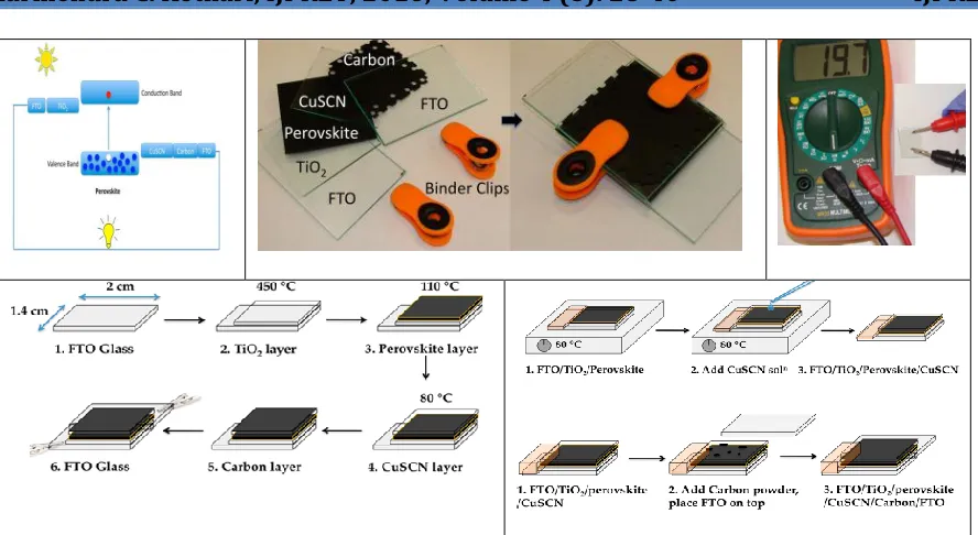
METHODOLOGY
The solar cell device consists of layers of titania (TiO2), perovskite (CH3NH3PbI3), copper
thiocyanate (CuSCN), carbon particles, sandwiched between two glass plates. The fabrication steps are depicted in Figure (3) with detailed as follows.
Step 1. Take a piece of FTO glass (2 cm × 1.4 cm), which is a piece of glass coated with transparent and conductive material, fluorine-doped tin oxide (FTO), on one side. Determine the conducting side using a multi meter.
Organized by C.O.E.T, Akola. Available Online at www.ijpret.com33
Figure (3):- A Physical Model & fabrication procedure for PEROVSKITE Solar Cell.
Step 3. Place the glass plate on the bench top with the FTO/TiO2 side facing up. Put
heat-resistant tape on the glass plate covering the bare FTO surface. Put one times to obtain a uniform smooth thin film.
Step 3 (with Drop). Place the glass plate on the benchtop with the FTO/TiO2 side facing up. Put
heat-resistant tape on the glass plate covering the bare FTO surface. Put one drop of perovskite precursor solution18 (0.5 M lead chloride +1.5 M methyl ammonium iodide in DMF) on the FTO/TiO2 film and spread it across the surface with a pipet. Roll it over the surface a few times
to obtain a uniform smooth thin film. Put the glass plate on the hot plate preheated to a temperature in the 90−120 °C range. After the film turns black, wait for at least 10 min before proceeding to Step 4.
Step 4. Turn the temperature of the hot plate down to 80°C. Put one drop of CuSCN solution (0.05 M CuSCN in dipropyl sulfide) and spread it across the surface with a pipet. Roll it over the surface a few times to obtain a uniform smooth thin film. Wait for 15 min and remove the glass plate from the hot plate.
Organized by C.O.E.T, Akola. Available Online at www.ijpret.com34 obtain a uniform film of carbon particles over it. The two FTO plates should be laterally shifted to make good electrical contacts and avoid a short circuit.
Figure (4):- Power conversion efficiency (PCE) of the solar cell is more than 15%.
At a main part of the solar cell, the organic-inorganic perovskite semiconductor (MeNH3PbI3)
can functionalize as an absorption layer.
RESULTS AND DISCUSSIONS
Two organolead halide perovskite nano-crystals, CH3NH3PbBr3 and CH3NH3PbI3, were found to
efficiently sensitize TiO2 for visible-light conversion in photo electrochemical cells. When
self-assembled on meso-porous TiO2 films, the nano-crystalline perovskites exhibit strong band-gap
absorptions as semiconductors. The CH3NH3PbI3-based photocell with spectral sensitivity of up
to 800 nm yielded a solar energy conversion efficiency of 3.8%. The CH3NH3PbBr3-based cell
showed a high photovoltage of 0.96 V with an external quantum conversion efficiency of 65%. The perovskite layer, with a band gap of 1.5 eV, absorbs light and creates electrons in the CB and holes in the VB. The TiO2 and CuSCN layers do not absorb visible light due to their wide band gap, but they exhibit significantly faster electron and hole transport, respectively. TiO2,
with its CB below the CB of perovskite, selectively transfers electrons from the perovskite’s CB to the FTO anode. Similarly, CuSCN, with its VB above the VB of perovskite, selectively transfers holes through the carbon particles to the FTO cathode. With electrons on the anode and holes on the cathode, the solar cell can power an external device, such as a LED.
Organized by C.O.E.T, Akola. Available Online at www.ijpret.com35 solubility, chemical reactivity, and stoichiometry. For deposition of the TiO2 layer (Step 2), we use a precursor solution containing titanium isopropoxide. In Table [2], the rA in APbX3 (X = Cl,
Br, I) perovskite was calculated for t = 0.8 and t = 1 based on effective ionic radii. A cations with radii between ∼1.60 Å and ∼2.50 Å were found to form perovskite structures. Thus, methyl-ammonium cation is suitable for lead halide perovskite because its ionic radius is 1.8 Å. Since the tolerance factor of CH3NH3PbI3was calculated as 0.83, deviation from an ideal cubic
structure is expected. Figure (5) shows the X-ray diffraction pattern of powder CH3NH3PbI3
formed from reaction between CH3NH3I and PbI2. The peaks were indexed as a tetragonal
phase with lattice parameters of a = b = 8.883 Å and c = 12.677 Å.
Table [2]:- Estimation of A cation radii in APbX3
r Pb Xa rAb for t = 0.8 rA b(Å) fort = 1.0
Pb2+(1.19 Å) Cl− (rCl = 1.81 Å)
Br− (rBr = 1.96 Å)
I− (rI = 2.20 Å)
1.58 Å
1.60 Å
1.64 Å
2.43 Å
2.50 Å
2.59 Å
a Effective ionic radii for coordination number of 6.
b rA = t × [√2(rB + rX)] − rX.
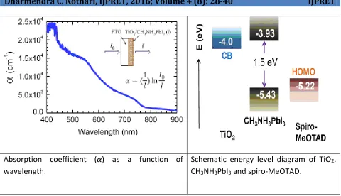
Optical band gap and absorption coefficient of CH3NH3PbX3, the absorption coefficient of
CH3NH3PbI3 was estimated from a nano-crystalline TiO2thin film surface coated with
CH3NH3PbI3. Figure (5) shows the absorption coefficient as a function of wavelength for the
CH3NH3PbI3 nano-dot-coated TiO2 film. The absorption coefficient was estimated to be 1.5 × 10⁴
cm−1 at 550 nm, indicating that the penetration depth for 550 nm light is only 0.66 μm. At 700
nm, the absorption coefficient was 0.5 × 104 cm−1, corresponding to a penetration depth of 2
Organized by C.O.E.T, Akola. Available Online at www.ijpret.com36 Absorption coefficient (α) as a function of
wavelength.
Schematic energy level diagram of TiO2,
CH3NH3PbI3 and spiro-MeOTAD.
Figure (5):- Absorption coefficient (α) as a function of wavelength for perovskite CH3NH3PbI3
nanodot coated with 1.4 μm TiO2 film (amount of adsorbed perovskite = 3.2 × 10⁴/μm2). A
was obtained from T = I/I0 = exp(−αl), where T, I, I0 and l represent transmittance, transmitted
light intensity, incident light intensity and TiO2 film thickness.
From ultraviolet photoelectron spectroscopy (UPS) and the Tauc plot obtained with UV–vis spectral data, valance band maximum (VBM), band gap, and conduction band minimum (CBM) for CH3NH3PbI3 were estimated to be −5.43 eV, −3.93 eV and 1.5 eV, respectively Figure (5).
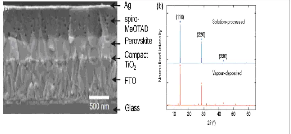
Perovskite solar cells were confirmed to work in the absence of a mesoporous TiO2 layer. As
shown in Figure (6), the CH3NH3PbI3−xClx thin layer coated Al2O3 film had a PCE of 10.9% [5]. The
Al2O3 served as a scaffold layer because electron injection from perovskite to Al2O3 was not
allowed. This result implies that the sensitization concept is not always required for perovskite solar cell design. Moreover, this result suggests that electron transfer can occur in the perovskite layer. A pillared structure was proposed in which the pores of a meso-porous TiO2
film (pillars) were filled with perovskite instead of a surface coating. As shown in (Figure 5), a thin capping layer (over layer) was formed after infiltration with the perovskite. With this method, PCE of 12% was reported using CH3NH3PbI3 and poly-triaryl-amine (PTAA), [6]. A higher
PCE of 15% was achieved from the pillared structure with a two-step coating procedure. In this method, the CH3NH3PbI3layer was prepared by dipping the PbI2 layer formed in meso-porous
TiO2 film into a diluted CH3NH3I solution while the perovskite layer was in contact with
Organized by C.O.E.T, Akola. Available Online at www.ijpret.com37 fabricated from junctions among the perovskite film (intrinsic layer), n-type thin TiO2 film, and
p-type HTM film. The planar pin junction concept, in which 300 nm-thick CH3NH3PbI3−xClx film
was prepared by co-evaporation of CH3NH3I and PbCl2, was confirmed to exhibit PCE over 15% [8]. Figure (6) shows a cross-sectional view of the planar structure in which the deposited
CH3NH3PbI3−xClx film shows only (hk 0) peaks in the X-ray diffraction pattern, indicating that Cl−
ions are located in an axial position, [7].
Figure (6):-Showing; (a) Cross-sectional sem image of planar pin junction structure with vapor-deposited CH3NH3PbI3−xClx. (b) X-ray diffraction patterns of vapour-deposited and
solution-processed CH3NH3PbI3−xClx. Impurity peaks corresponding to un-reacted species are
presented in the vapour-deposition process.
Overall, perovskite solar cells offer great variability. A combination of different electron/hole-transporting materials and light-absorbing perovskites could be used to fabricate solar cells. Instead of using planar device structure, an additional layer of meso-porous TiO2 or Al2O3 on
FTO/TiO2 could be used to fabricate perovskite cells. Different solution deposition techniques
could be used to obtain the perovskite film.
FUTURE DIRECTION and CHALLENGES
Recent progress in perovskite solar cells based on organolead halides has been reviewed here. CH3NH3PbI3 and mixed halide perovskite CH3NH3PbI3−xClx are at the center of research into high
Organized by C.O.E.T, Akola. Available Online at www.ijpret.com38 still possible through structural modification, along with band gap tuning. Modification of the bond distance and/or angle of X–Pb–X in CH3NH3PbX3 is one of strategies to tune band gap
energy. More recently, a PCE approaching 30% was achieved from a single junction perovskite solar cell. Optimistic expectations for the perovskite solar cell are based on the superb opto-electronic property of organo metal halide perovskite material that is even better than high efficiency GaAs. Since the high Voc observed from organo metal halide perovskite is likely to be
related to high internal photoluminescence quantum efficiency, careful control of the luminescent property of perovskite could further improve Voc, hence contributing to an even
higher PCE. For commercialization, environmental and photo-stabilities should be guaranteed. For this to be achieved, encapsulation technology and materials with humidity-resistance and photo-stability must be developed. Scale-up technologies for high efficiency module fabrication are also an important challenge. Finally, substitution of other elements for Pb is one of the important tasks for environmentally friendly perovskite solar cells.
CONCLUSIONS
Many different photovoltaic technologies are being developed for large-scale solar energy conversion. The wafer-based first-generation photovoltaic devices have been followed by thin-film solid semiconductor absorber layers sandwiched between two charge-selective contacts and nano-structured (or meso-structured) solar cells that rely on a distributed hetero-junction to generate charge and to transport positive and negative charges in spatially separated phases. Although many materials have been used in nano-structured devices, the goal of attaining high-efficiency thin-film solar cells in such a way has yet to be achieved. Organo-metal halide perovskites have recently emerged as a promising material for high-efficiency nano-structured devices.
We analyzed the crystallization process of the CH3NH4PBI, perovskite by observing real time
X-ray diffraction immediately after combining a PBI2 thin film with a CH3NH4I solution. A detailed
analysis of the transformation kinetics demonstrated the fractal diffusion of the CH3NH4I
solution into the PbI2 film. Moreover, the perovskite crystal was found to be initially oriented
based on the PbI2 crystal orientation but to gradually transition to a random orientation. The
Organized by C.O.E.T, Akola. Available Online at www.ijpret.com39 cell, the organic-inorganic perovskite semiconductor (MeNH3PbI3) can functionalize as an
absorption layer.
REFERENCE
1. Beiley, Z. M. & McGehee, M. D., (2012), “Modeling low cost hybrid tandem photovoltaics with the potential for efficiencies exceeding 20%. Energy Environ. Sci.5, 9173–9179.
2. Chavhan, S.; Miguel, O.; et. al., (2014), “Organo-Metal Halide Perovskite-Based Solar Cells with CuSCN as the Inorganic Hole Selective Contact”, J. Mater. Chem. A, 2, 12754−12760.
3. Cheng, Z. & Lin, J. , (2010), Layered organic–inorganic hybrid perovskites: structure, optical properties, film preparation, patterning and templating engineering. CrystEngComm.12, 2646– 2662.
4. Dar, M. I.; Arora, N.; et.al, (2014), “Investigation Regarding the Role of Chloride in Organic Inorganic Halide Perovskites Obtained from Chloride Containing Crecursors”, Nano Lett. 14, pp. 6991−6996.
5. Lee, M. M.; Teuscher, J., et. al., (2012), “Efficient Hybrid Solar Cells Based on Meso-Superstructured Organometal Halide Perovskites”, Science, 338, pp. 643−647.
6. Liu, M. Z.; Johnston, M. B., (2013), “Efficient Planar Hetero-junction Perovskite Solar Cells by Vapour Deposition”, Nature, 501, pp. 395−398.
7. Oku, T., (2012), “Direct structure analysis of advanced nano-materials by high resolution electron microscopy”, Nanotechnology Reviews, Vol. 1, pp. 389–425.
8. Qin, P.; Tanaka, S., (2014), “Inorganic Hole Conductor-Based Lead Halide Perovskite Solar Cells with 12.4% Conversion Efficiency”, Nat. Comun. 5, pp. 3834.
9. Oku, T., (2014), “Structure analysis of advanced nanomaterials: nano-world by high– resolution electron microscopy”, Walter De Gruyter Inc. Germany.
10. Sukhatme, S.P. & Nayak, J.K., (2009), “SOLAR ENERGY, Principles of Thermal Collection and Storage”, Third Edn., The McGraw Hill Co. Ltd., New Delhi.
11. Wakamiya, A., Endo, M., Murata, Y., (2014), “Reproducible fabrication of efficient perovskite-based solar cells: X-ray crystallographic studies on the formation of CH3NH3PbI3
![Figure (1):- ABX3 perovskite structure showing BX6 octahedral and larger A cation occupied in cubo-octahedral site and Unit cell of cubic CH3NH3PbI3 perovskite, [1]](https://thumb-us.123doks.com/thumbv2/123dok_us/8709751.1740730/2.612.76.539.217.373/figure-perovskite-structure-showing-octahedral-occupied-octahedral-perovskite.webp)
![Table [1]:- The development of types of Solar Cells with their efficiency.](https://thumb-us.123doks.com/thumbv2/123dok_us/8709751.1740730/4.612.74.542.44.318/table-development-types-solar-cells-efficiency.webp)