Available Online at www.ijpret.com 1049
INTERNATIONAL JOURNAL OF PURE AND
APPLIED RESEARCH IN ENGINEERING AND
TECHNOLOGY
A PATH FOR HORIZING YOUR INNOVATIVE WORKDESIGN AND SIMULATION OF UNIVERSAL ASYNCHRONOUS RECEIVER
TRANSMITTER ON FIELD PROGRAMMABLE GATE ARRAY USING VHDL
MR. MANGESH V. BENODKAR1, PROF. UMESH W. HORE2
1.Student of M.E., Department of Electronics & Telecommunication Engineering, P. R. Patil College of Engineering, Amravati, Maharashtra – India.
2.Faculty of Electronics & Telecommunication, Department of Electronics &Telecommunication Engineering, P. R. Patil College of Engineering, Amravati, Maharashtra – India.
Accepted Date: 05/03/2015; Published Date: 01/05/2015
\
Abstract: This paper concentrates on the design of Universal Asynchronous Receiver and Transmitter (UART) using VHDL. A UART is a full duplex receiver/transmitter. UART includes three modules which are received, the baud rate generator and transmitter. The UART design with Very High Description Language can be integrated into the Field Programmable Gate Array to achieve reliable, compact & stable data transmission. It’s significant for the design of System on Chip (SOC). It is the microchip with programming that controls a computer's interface to its attached serial devices. It handles the conversion between serial and parallel data. It is the most widely used serial data communication circuit ever. Whole process of serial transmission is based upon the principle of shift register. In the result and simulation part, this paper will focus on check the receive data with error free &baud rate generation at different frequencies.
Keywords:VHDL, FPGA, Xilinx ISE
Corresponding Author: MR. MANGESH V. BENODKAR
Access Online On:
www.ijpret.com
How to Cite This Article:
Mangesh V. Benodkar, IJPRET, 2015; Volume 3 (9): 1049-1056
Available Online at www.ijpret.com 1050
INTRODUCTION
Asynchronous serial communication has advantages of less transmission line, high reliability, and long transmission distance, therefore is widely used in data exchange between computer and peripherals. Asynchronous serial communication is usually implemented by Universal Asynchronous Receiver Transmitter (UART). UART allows full-duplex communication in serial link, thus has been widely used in the data communications and control system [5]. A Universal Asynchronous Receiver Transmitter includes a transmitter and a receiver. The transmitter is essentially a special shift register that loads data in parallel and then shifts it out bit by bit at a specific rate. The receiver, on the other hand, shifts in data bit by bit and then reassembles the data. UART transmitter controls transmission by fetching a data word in parallel format and directing the UART to transmit it in a serial format. Likewise, the Receiver must detect transmission, receive the data in serial format, strip of the start and stop bits, and store the data word in a parallel format. Since the UART is asynchronous in working, the receiver does not know when the data will come, so receiver generate local clock in order to synchronize to transmitter whenever start bit is received. Asynchronous transmission allows data to be transmitted without the sender having to send a clock signal to the receiver. In actual applications, usually only a few key features of UART are needed. Specific interface chip will cause waste of resources and increased cost. Particularly in the field of electronic design, SOC technology is recently becoming increasingly mature. This situation results in the requirement of realizing the whole system function in a single or a very few chips. Designers must integrate the similar function module into FPGA [2].
This paper uses the VHDL language to implement the core functions of UART and integrate the min to a FPGA chip. In this we also design for different baud rate UART for synchronization of transmitter to receiver through PL2303by using FPGA starter kit.
I.
Design ModuleAvailable Online at www.ijpret.com 1051
the Least Significant Bit (LSB) being sent first. Each bit in the transmission is transmitted for exactly the same amount of time as all of the other bits, and the receiver “looks” at the wire at approximately halfway through the period assigned to each bit to determine if the bit is a 1 or a 0. When the entire data word has been sent, the transmitter may add a Parity Bit that the transmitter generates. The Parity Bit may be used by the receiver to perform simple error checking. Then at least one Stop Bit is sent by the transmitter. When the receiver has received all of the bits in the data word, it may check for the Parity Bits (both sender and receiver must agree on whether a Parity Bit is to be used), and then the receiver looks for a Stop Bit. Regardless of whether the data was received correctly or not, the UART automatically discards the Start, Parity and Stop bits. If the sender and receiver are configured identically, these bits are not passed to the host. If another word is ready for transmission, the Start Bit for the new word can be sent as soon as the Stop Bit for the previous word has been sent.
A. Receiver module:
In UART serial communication, receiver accepts the data serially and sends at the output in parallel manner. Basically receiver has clk_out, reset and RxD input lines where clk_out gives continuous clock to receiver and from Rxd line serial data can be given. At the output level received data can obtained in parallel manner. The UART communication format consists of a start bit followed by 8 data bits and one stop bit indicating the end of the communication. This block monitors the input line for new data which is indicated by the start bit. When the load signal is high it will get the start bit from the transmitter which assures that the original data is now being send by the transmitter. Once the shift signal is becomes high with no load signal, the data coming from the transmitter gets shifted into the intermediate register of the receiver and provides the 8 bit serial data which we have given as an input to the transmitter. Once the entire data has been sent the parity error and the CRC errors has been checked out and are served as the input to the transmitter. If parity error and CRC errors occur or are at logic 1, it means that our transmission is having some errors.
B. Baud rate generator:
Available Online at www.ijpret.com 1052
very critical to determine where to sample the data information. The ideal time for sampling is at the middle point of each serial data bit.
These are some standard baud rates which we have used in our design,
S0 S1 S2 Baud Rate(BPS)
0 0 0 600
0 0 1 1200
0 1 0 2400
0 1 1 4800
1 0 0 9600 (default)
1 0 1 14400
1 1 0 19200
1 1 1 38400
C. Transmitter module:
The function of transmit module is to convert the sending 8-bit parallel data into serial data, adds start bit at the head of the data as well as stop bits at the end of the data. The function of the transmitter module is to convert the 8 bit serial data into the single bit data. In this module, when our load signal is high the data in stored into the holding register. The data in the holding register is shifted to the intermediate register with the start bit of zero and this intermediate register is of 9 bits. Once the shift signal is high the least significant bit of the intermediate register i.e. the start bit comes at the output of the transmitter and served as the input to the receiver. When the entire data has been sent, the transmitter provides a parity bit which is served as the input to the receiver.
D. Field Programmable Gate Arrays:
Available Online at www.ijpret.com 1053
(HDL) to specify how the chip should work. FPGAs have programmable logic components called ‚logic blocks‛, and a hierarchy or reconfigurable interconnects which facilitate the ‚wiring‛ of the blocks together. The programmable logic blocks are called configurable logic blocks and reconfigurable interconnects are called switch boxes. Logic blocks (CLBs) can be programmed to perform complex combinational functions, or simple logic gates like AND and XOR. In most FPGAs the logic blocks also include memory elements, which can be as simple as a flip-flop or as complex as complete blocks of memory. Advantages of FPGA are as follows:
Ability to re-program in the field to fix bug.
Fast prototyping and turn-around time.
NRE cost is zero.
High-Speed.
Low cost.
II.
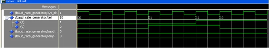
Simulation result of module1. Simulation result of Baud rate generator:
The simulation result shows the serial transmission and reception of 8 bit data. As shown in figure we have selected S0=1 and S1=0 to select the baud rate of 19200bps. It shows the continuous output for the selected baud rate.
Figure 3.1: Simulation result of Baud rate generator
2. Simulation result of Receiver module:
Available Online at www.ijpret.com 1054
Figure 3.2: Simulation result of Receiver module
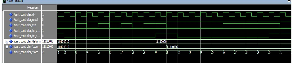
3. Simulation result of Transmitter module:
Figure 3.3 shows simulation of transmitter module. From simulation waveform, as changes happen on "txd" lines that parallel data is stored in shift register and gives serial data which contains start bit, data bit(8) and Stop bit.
Figure 3.3: Simulation result of Transmitter module
III.
ResultAvailable Online at www.ijpret.com 1055
Figure 4.1: synthesis result
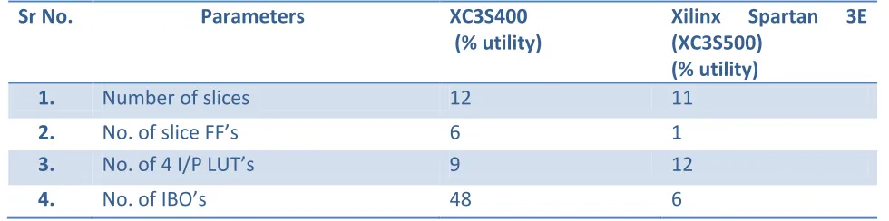
Comparison of the utilization of FPGA space in different device:-
Sr No. Parameters XC3S400
(% utility)
Xilinx Spartan 3E
(XC3S500) (% utility)
1. Number of slices 12 11
2. No. of slice FF’s 6 1
3. No. of 4 I/P LUT’s 9 12
4. No. of IBO’s 48 6
IV.
ACKNOWLEDGMENTI would like to acknowledge the Faculties of Electronics & Telecommunication Department, P.R. Patil College of Engineering &Technology, and Amravati for their support. I Mangesh V. Benodkar specially want to thank my guide Professor U. W. Hore sir for their valuable guidance and constant encouragement towards the work.
REFERENCES
1. GarimaWakhle; itiagrawalet; “Synthesis and Implementation of UART using VHDL Codes”, IEEE 2012, DOI 10.1109/IS3C.2012.10.
Available Online at www.ijpret.com 1056
3. Bhavna manure and Rahul tanwar, “UART with automatic baud rate generator and frequency divider” Journal of Information Systems and Communication on 15 Feb 2012.
4. Naresh Patel, Vatsalkumar Patel, “VHDL Implementation of UART with Status Register”, IEEE JOURNAL in 2012, DOI 10.1109/CSNT.2012.164