Comparative study on microfluidic performance of ZnO surface acoustic wave
devices on various substrates
Wenbo Wanga, Xingli Hea, Jian Zhoua, Hang Gua, Weipeng Xuana, Jinkai Chena,
Xiaozhi Wanga* and J.K. Luoa,b*
a
Dept. of Info. Sci. & Electr. Eng., Zhejiang University and Cyrus Tang Center for Sensor
Materials and Applications, 38 Zheda Road, Hangzhou 310027, China. b
Institute of Renewable Energy & Environ. Technol., University of Bolton, Deane Road,
Bolton, BL3 5AB, United Kingdom
In recent years, lab-on-a-chip (LOC) technology has attracted great attentions for research
and development, and has been widely utilized in chemical, biological and medical
applications.1-8 Microfluidics including liquid transportation, pumping, mixing, digitizating
etc, and sensors are the two main components of LOC microsystems. Various effects have
been utilized to develop microfluidics such as bimorph structure, electrostatic and
piezoelectric mechanisms. Moving part-free microfluidics based on kinetic energy such as
electroosmosis,9, 10 electrophoresis,11, 12 dielectrophoresis13, 14 etc are preferred owing to its
advantages of excellent reliability, easy fabrication and operation etc.
Surface acoustic wave (SAW) device is one of the building blocks for electronics and
microsystems,15-17 and can also be utilized for accurate sensing, efficient fluidic actuation and
manipulation.18-23 Therefore SAW-based microfluidic devices and sensors will play an
important role in single mechanism based-LOCs in the future. SAW-based microfluidics have
the advantages of low cost, high stability, easy fabrication and operation,24 and have been
intensively investigated and studied in recent years. Wixforth demonstrated the principle of
SAW-based microfluidic.25 Li et al demonstrated the particle concentration effect on LiNbO3
substrate26 and Alghane et al conducted numerical simulation for liquid mixing and particle
concentration.27 They also discussed the frequency effect and scaling effect on the
performance of SAW-based microfluidics.28, 29 Shi et al showed that standing surface acoustic
wave (SSAW) can be used for particle sorting and manipulation.30 Reboud et al reported the
ability to do cell lyses using SAW on LiNbO3 substrate.31
One of the key issues for widespread application of LOCs and microfluidics is the cost of
the materials and devices involved, which is the same for the SAW-based microfluidics and
LOCs. At the early study, SAW-based microfluidic devices were all made on single
crystalline bulk piezoelectric materials such as LiNbO3, LiTaO3, that are relatively expensive,
and signal processing. ZnO thin films on silicon (Si) substrate were then introduced for the
development of thin film SAW-based microfluidics, and demonstrated its great potential for
LOC application.32-34 Du et al demonstrated the thickness effect of the piezoelectric layer on
the ZnO/Si-based SAW devices, and characterized its microfluidics performance.35, 36
Recently, we have developed flexible ZnO thin film SAW devices on polyimide (PI)
substrates37 and showed these devices can deliver the microfluidic functions as those by the
ZnO/Si SAW devices. Furthermore, we have developed the transparent SAW devices using
ZnO thin films deposited on glass substrates,37-39 demonstrated their comparable transmission
properties to that on crystalline Si substrate. The materials for the PI and glass substrates are
abundant and cheap; furthermore they are disposable, flexible or transparent, and thus have
much better potential for LOC and microfluidic applications. In this work, we conducted a
systematic investigation on SAW-microfluidics based on these three substrates (Si, glass and
PI), and compared their performances.
Experimental
Piezoelectric thin film deposition.— ZnO thin films were used as the piezoelectric layer,
and were deposited on silicon, glass (Corning 2318) and polyimide (Kapton® polyimide film
100 H) substrates, with a direct-current (DC) magnetron sputtering deposition system. Si
substrate was (100) orientation and 4 inch in diameter. The thickness of Si, glass and PI
substrates was 500 μm, 500 μm and 100 μm, respectively. The deposition conditions used
were optimized previously37, 39 as follow: A zinc target with 99.999% purity was used for
ZnO deposition; the chamber pressure was 1 Pa, and Ar/O2 mixture at a ratio of 100/50 (sccm)
was used. The distance between the target and substrate was set to be 70 mm, and the
substrate temperature was fixed at 200 °C. The sputtering power was set to be 200 W and the
bias voltage was -75 V. The deposition rate was ~13 nm/min and the thickness of all the films
Crystal structure characterization.— X-ray diffraction (XRD) (Panalytical Empyrean)
with Cu-kα radiation (λX = 0.154 nm) at 40 keV and 40 mA was used for analyzing the
crystalline structure, a diffraction pattern was obtained with a 25°-60° 2θ angle. Scanning
electron microscope (SEM) (Hitachi S-4800) was used for cross-sectional structure analysis
with a 3 keV acceleration voltage. For surface roughness characterization, atomic force
microscopy (AFM) (SPI-3800N, Seiko Co.) in a tapping mode was used.
SAW device fabrication.— Ultraviolet light photolithograph and lift-off process were used
to make interdigitated transducers (IDTs). An 80 nm thick Al film was used to fabricate IDTs
which have 100 pairs of fingers, 12 μm wavelength (λ) and 3 mm aperture.
SAW device measurement and numerical simulation.— A network analyzer (E5071C,
Agilent) was used to characterize the transmission and reflection property of the devices.
Numerical study was also carried out to analyze the wave propagation mode with finite
element analysis (FEA) using COMSOL MultiPhysics 3.5a (Comsol Ltd.) software. A model
with the periodic boundary condition and ideal material properties was used for the modeling.
Acoustic microfluidics testing.— In this study, a signal generator (SMIQ 03B,
ROHDER&SCHWARZ) connected to an RF amplifier was utilized to apply the RF signal to
the device. Deionized (DI) water droplets mixed with polystyrene microparticles (~7 μm in
diameter) were used for microfluidic measurement, and the volume was controlled by a
micropipette ranging from 2 μl to 10 μl. It was loaded at the center of the SAW path when
measuring acoustic streaming velocity and at the edge of wave path asymmetrically for
particle concentration experiments. The movement of microparticles and fluid streaming were
captured by a high speed camera (Grasshopper 03K2C, with 200 frames per second) for
detailed analysis.
Results and discussions
deposited film for the initial deposition at the thickness of a few tens of nanometers, but the
films tend to be similar as they grow thicker. The crystal structures and properties of the ZnO
films are hardly affected by the substrate material but by the deposition conditions owing to
the thick ZnO layer used for all the samples. The ZnO films on different substrates show very
similar properties with no noticeable difference. As a representative, Figure 1 shows the
characterization results of ZnO thin film deposited on glass substrate. The SEM image
illustrates that the ZnO crystal has a columnar grain structure, tightly packed with no void.
The roughness of the ZnO films obtained by AFM measurement is 6 nm, 6 nm and 10 nm for
the ZnO layers on Si, glass and PI substrates respectively, implying that all the ZnO thin films
are suitable for fabricating devices by planar process. The XRD curves exhibit a strong and
sharp peak at about 34.2° for the films on all three types of substrates, showing the excellent
(0002) crystal orientation for all the films. The deviation of the peak positions from the
standard 34.42° of monocrystal ZnO39 is caused by the in-film stress, which is in the order of
1.2~1.4 GPa for all the films used here. Although post-annealing at temperatures >200 °C
could release the stress,40 we only compared the as-deposited films here due to the
temperature limitation of the PI substrate. The full-width at half maximum (FWHM) for the
(0002) ZnO peak is 0.18°, 0.19° and 0.18° for the ZnO films on Si, glass and PI substrates,
respectively. The grain size of the ZnO films estimated by the Debye–Scherrer formula39, 41 is
48.2 nm, 45.7 nm and 51.2 nm for the ZnO films on Si, glass and PI, respectively, that are
comparable to those well-performed ZnO films reported in other works42, 43.
Transmission characteristics.— The ZnO thin film devices fabricated on three substrates
are showed in Figure 2. It is apparent that SAW devices on both the glass and PI substrates
have good transparency, while those on PI have excellent flexibility, showing these devices
are suitable for the development of transparent and flexible electronics and LOCs. The
of the substrates are shown in Figure 3. For the ZnO/Si device, two resonant peaks can be
observed from both the reflection and transmission spectra at the frequency of 260.3 and
424.4 MHz, respectively. The former is the Rayleigh (R) mode, and the peak amplitude is
weak due to the high normalized thickness ratio of hk~2.09 (h is the ZnO thickness and
k=2π/λ).36 The higher frequency peak is the Sezawa (S) mode as expected from the structure
with a higher acoustic velocity in the substrate than in the overlay. The S mode is much
stronger than the R mode, indicating more acoustic energy could be obtained from the S
mode wave for microfluidic application. For the ZnO/glass device, only the R mode wave
(214.2 MHz) could be observed. This is because the acoustic velocity in the glass and ZnO
are very close (~3200 m/s and ~2700 m/s)33, 44 to each other. The devices on the ZnO/PI show
resonant peaks at the frequencies of 150.4 and 414.3 MHz, respectively. The former one
corresponds to the R mode wave, while the latter is the Lamb (L) mode wave as discussed in
details in our previous work.37
To further identify the wave modes of the devices, numerical simulation was carried out
for these devices. The 2-dimensions FEA modeling uses the actual scale of the devices with
periodic boundary. The deformation of the device structures at various resonant modes is
shown in Figure 4. For the silicon and glass substrates, the deformation shape for the R mode
is similar, acoustic waves mainly propagate on the surface layer (within about one
wavelength depth), consistent with the feature of typical SAW. Owing to much higher
acoustic velocity in Si than that in ZnO, a Sezawa mode could be found for the device on
silicon, but not for that on glass. A large deformation occurs in the ZnO/PI for both the R and
L modes due to the lower elastic modulus of the PI substrate. For the R mode, the largest
deformation is confined in the surface, in agreement with the R mode on the Si and glass. In
Figure 4(e), the deformation shape in substrate is symmetric, which is similar to the
The detail analysis about wave velocity of the L mode for PI can be found in our previous
paper ref.37.
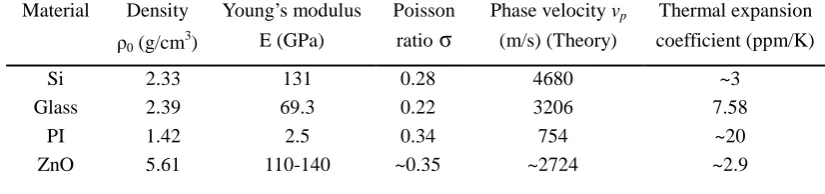
Table I. Characteristics of ZnO based SAW devices on Si, glass and PI substrates
Material Density ρ0 (g/cm3)
Young’s modulus E (GPa)
Poisson ratioσ
Phase velocity vp
(m/s) (Theory)
Thermal expansion coefficient (ppm/K)
Si 2.33 131 0.28 4680 ~3
Glass 2.39 69.3 0.22 3206 7.58
PI 1.42 2.5 0.34 754 ~20
ZnO 5.61 110-140 ~0.35 ~2724 ~2.9
The phase velocity, wavelength and resonant frequency are correlated by v = λf. The phase
velocity of all the wave modes can be calculated using this equation with the results
summarized in Table II. For dual layer structures, acoustic waves propagate in both the ZnO
layer and substrate as the thickness of ZnO is much less than one wavelength, therefore the
phase velocity of the R mode is strongly affected by both the substrate material and ZnO film.
The phase velocity of the fundamental mode (the R mode) in Si is 4680 m/s.36 These in
Corning glass and PI substrates can be calculated by the following equation37
𝑣𝑝 = 0.93�E 2(1 +⁄ σ)ρ0 (1)
where E is the Young’s modulus, σ presents the Poisson’s ratio and ρ0 is the density of
material. Those values could be found from the material datasheet (list in Table I),33, 37, 46-50
and the calculated phase velocity for ideal bulk glass and PI is 3206 m/s and 754 m/s,
respectively. The experimentally obtained phase velocity for the R-mode in the ZnO/Si is
3123, much smaller than the ideal case due to the influence of ZnO layer with slower phase
velocity. For the SAW on PI, the velocity for the R-mode is larger than than in the PI layer as
the velocity in the ZnO is much larger. The detailed discussion about the phase velocities in
ZnO/PI SAW devices can be found from our previous publication ref.37.
laoding a 4 μl droplet on the wave path, demonstrating that the acoustic energy is almost
completely coupled into the fluid. For microfluidic application, it is apparent that SAW with
larger signal amplitude and less insertion loss are desirable as more acoustic energy and large
force can be utilized for application. The insertion loss of all the devices is summarized in
Table II. The S mode of the ZnO/Si devices has a similar insertion loss to that of the R mode
wave, but the peak amplitude is much larger, indicating the S mode is more suitable for
developing microfluidic devices. Larger insertion loss is observed for the R mode of the
ZnO/glass device as compared to those on Si substrate, but its resonant peak also has a large
amplitude, implying a comparable performance with that of the ZnO/Si devices. For the
ZnO/PI devices, both the R and L modes have large insertion loss (-45.815 dB and -43.647
dB, respectively), implying the energy transmission would be poor and may be inferior for
microfluidic application. The electromechanical coupling coefficients (k2) calculated from the
reflection measurements32 are also presented in Table II for comparison. For the ZnO/Si
devices, the k2 value of the S mode is about 5.07%, much larger than that of the R mode,36
implying that the S mode can deliver better microfluidic function. For both the ZnO/glass and
L mode of ZnO/PI devices, the k2 values are around 1.0%,37, 38 and the value of the R mode of
the ZnO/PI is the smallest.
TableII. Characteristics of ZnO based SAW devices on Si, glass and PI substrates
Substrate Wave mode
f0
(MHz)
Insertion loss (dB)
K2 (%) TCF (ppm/K)
Phase velocity (m/s) (experim.) Si Rayleigh 260.3 -8.448 0.66 -41 3123.6 Si Sezawa 424.4 -8.659 5.07 -48 5092.8 Glass Rayleigh 214.2 -14.596 1.05 -38 2570.4 PI Rayleigh 150.4 -45.815 0.58 -310 1804.8 PI Lamb 414.3 -43.647 1.06 -143 4971.6
Although the Young’s modulus is similar for silicon and glass, Si is monocrystal while
ZnO/Si devices work better than the ZnO/glass ones. The lower modulus of PI compared
with those of Si and glass induces much larger acoustic attenuation in the PI substrate and
acoustic impedance mismatch at the ZnO/substrate interface. Additionally, large roughness of
the PI surface also makes stronger scattering of acoustic wave, which increases the loss. That
makes the ZnO/PI devices not as good as the other two types. The above results clearly show
that substrate has an obvious effect on the transmission performance of devices. The
difference in material properties, hence the acoustic transmission would finally determines
their microfluidic performance. In combination, it is clear that the ZnO/Si and ZnO/glass
devices would be more competitive than that of the ZnO/PI devices for microfluidic
applications.
Temperature effect for different substrates.— The resonant frequency shift versus
temperature was investigated for all types of the devices with the results shown in Figure 6.
The temperature coefficient of frequency (TCF), defined as Δf/ΔTf0, can be calculated from
the gradients of the lines in Figure 6 and is presented in Table II. The TCF value is less than
-50 ppm/K for both the wave modes of the ZnO/Si devices,51 and is about -38 ppm/K for the
ZnO/glass devices, which is consistent with the result obtained from the Al-doped ZnO
transparent SAW devices.38 The TCFs of the ZnO/Si and ZnO/glass are smaller than that (-75
~ -80 ppm/K) of LiNbO3 SAW devices,18 while those of the ZnO/PI are much larger.
The TCF is influenced by both temperature coefficient of acoustic velocity and thermal
expansion coefficient, and is expressed as follows,52
TCF = 1𝑓∂𝑓∂T= 𝑣1
𝑝
∂𝑣𝑝
∂T − 1 𝜆
∂𝜆 ∂T=
1 𝑣𝑝
∂𝑣𝑝
∂T − 𝛼 (2)
where f is the resonant frequency, T temperature, and α the thermal expansion coefficient. The
large TCF of the SAW on PI is mainly caused by the very large α of the PI substrate. The
velocity change with temperature is mostly determined by the temperature coefficient of
suppress thermal expansion of the ZnO thin film more effectively.54 As a result, SAW on Si
and glass substrates have smaller TCFs than that of PI. It should be pointed out that residual
stress (strain) in the film also plays an important role in TCF.55 But it seems to have limited or
the same effect on the difference of the TCFs obtained as the residual stress is similar for all
the devices as confirmed by the shift of the (0002) peak in the XRD curves.
Although high TCF is good for the development of high sensitivity temperature sensors, it
is not desirable for microfluidic application as a part of acoustic energy will be wasted as the
thermal energy; meanwhile it requires a tracking circuitry to monitor and adjust the RF
frequency to match the frequency change caused by the raised temperature for applications.
Comparison of acoustic streaming.— It is well known that SAW could induce acoustic
streaming when liquid is on the forward path of acoustic waves as schematically shown in
Figure 7. Acoustic streaming is a basic but useful function of SAW-based microfluidics; it can
pump and transport liquids, and provide efficient mixing,27 which is a very challenging task
for micro-liter scale fluids.
The performances of ZnO-based SAW devices of different wave modes were measured and
compared. The acoustic streaming as shown in Figure 7(c) can be seen from all our SAW
devices. The variation of streaming velocity as a function of RF signal voltage is presented in
Figure 8. With the same liquid volume of 2 µl, the ZnO/Si device show the highest streaming
velocity, especially for that by the Sezawa mode, consistent with the observation by Du et
al.35 The ZnO/glass devices achieve a streaming velocity more than 5 cm/s, comparable to
that of the ZnO/Si ones. The ZnO/PI devices exhibit the poorest performance among the three
types of the devices, as expected from the transmission properties discussed above. The main
reason is due to the large acoustic absorption by the PI substrate, which makes a remarkable
attenuation of the transmission energy.
15 cm/s streaming velocity in less than 2.5 V signal voltage. Compared with those, the ZnO
devices showed above have poorer performance. However, except for special applications
such as nebulization, droplet-ejection etc,57, 58 microfluidic functions such as mixing and
transportation etc only need low fluid velocity, in the order of several tens to hundreds of
micrometers per second.59, 60 Thus the streaming performance of the ZnO SAW-based devices
on all three substrates are competitive and promising for the microfluidic application.
Comparison of particle concentration.— Controlled particle manipulation and
concentration have a lot of applications in biochemical analysis and medical researches as it
can significantly improve the sensitivity to target substances such as proteins, cells61 and
bacteria.30 It has been well studied that asymmetric SAW induced streaming could induce
micro or nano-particle concentration.26, 27 Figure 9 illustrates the principle of the SAW-based
microparticle concentration. With the droplet located on the edge of the wave path, the
acoustic force would induce a single vortex streaming within the droplet, moving the
microparticles toward the center of the vortex.26, 27 The microimages in Figure 9(c) - 9(e)
show that the polystyrene microparticles moved into the central area with an excellent
efficiency after applying SAW at 0, 5 and 10 sec for the ZnO/glass SAW device.
The particle concentration on the ZnO/PI devices has been studied in our previous work.37
Due to the weak transmission of the SAW on PI substrate, the time for particle concentration
is very long, typically over 50 sec, and the concentration efficiency is relatively poor
compared to those induced by SAW on other two types of substrates. For example, as shown
in ref.37, under an RF signal of Vpp (peak-to-peak voltage) 25 V, 70 sec were needed to
concentrate the microparticles. Here we mainly discuss the particle concentration results from
the ZnO/Si and ZnO/glass devices.
With a ~4 μl droplet and a 12.8 Vpp signal voltage, the particle concentration performance
initial (the diameter of the droplet) and the concentrated particle distribution, Dc/Dt, to
characterize the concentration process. We define the time at Dc/Dt = 0.1 as the concentration
time. In Figure 10(a), it can be seen that for all the wave modes, the relationship between
Dc/Dt and time is nonlinear when the signal amplitude increases; Dc/Dt decreases rapidly at
the beginning and then slow down. The S mode of the ZnO/Si devices work the best for
particle concentration owing to the low insertion loss and high k2. Comparion of the devices
on the two types of the substrates, it is clear that the ZnO/Si device has a higher efficiency,
but the difference is quite small. Figure 10(b) shows the concentration time as a function of
signal voltage. Note that for all the wave modes in both the substrates, even with the smallest
signal voltage, the concentration time is less than 10 sec, that is very quick and sufficient for
LOC application.
Since ZnO/glass devices worked well, detailed experiments were conducted to investigate
the influence of droplet volume on the particle concentration performance. The liquid volume
was varied from 4 μl to 10 μl with the results shown in Figure 11. The concentration time
remain almost unchanged at about 10 sec when the liquid volume is changed from 4 to 10 µl.
Hence, we can conclude that for particle concentration application, ZnO/glass devices have a
comparable performance to the ZnO/Si devices, and may play more important role in LOC
application as the glass substrate is cheap, disposable, and widely used for biochemical
analysis.
In general, SAW devices based on bulk piezoelectric substrate perform better than those
using piezoelectric thin films, and can deliver better functions in microfluidics such as high
streaming velocity and short particle concentration time. For instance, LiNbO3 SAW devices
can concentrate microparticles at less than 20 dB power (~7 Vpp, estimation based on a 50 Ω
matching resistor),27,62,40 better than these reported here. However, as mentioned above, very
the wavelength of SAW can significantly improve the particle concentration efficiency as
discussed with King’s equation63 by Rogers et al,62 and use of focused IDT SAW will also
offer a better option for microfluidics.64 These can help to overcome the shortages of the thin
film SAW devices.
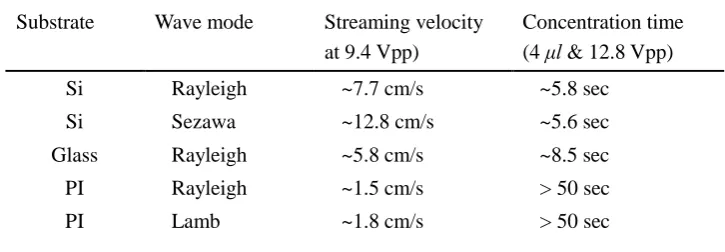
Table III. Comparison of microfluidics performance.
Substrate Wave mode Streaming velocity at 9.4 Vpp)
Concentration time (4 μl & 12.8 Vpp)
Si Rayleigh ~7.7 cm/s ~5.8 sec
Si Sezawa ~12.8 cm/s ~5.6 sec
Glass Rayleigh ~5.8 cm/s ~8.5 sec
PI Rayleigh ~1.5 cm/s > 50 sec
PI Lamb ~1.8 cm/s > 50 sec
Table III is the comparative summary of the microfluidic performances of the SAW
devices on three types of substrates. From performance point of view, the S mode of ZnO/Si
SAW is the best, and is followed by the R mode of both the ZnO/glass and ZnO/Si SAW
devices, and then those on PI substrate. The cost for Si substrate is higher than other two, but
it has the advantages of the option for the integration with electronics on the same substrate.
Glass substrate is one of the base materials for many biochemical analysis, DNA and protein
microarrays, LOCs and microfluidics etc. Effective utilization and integration of SAW-based
microfluidics and SAW sensors on a glass substrate with other components would greatly
increase and enhance many functions for biochemical analysis. For example, integrated SAW
can be utilized to study cell growth and mutation under acoustic stimulation65. Glass substrate
also is transparent, a property Si lacks, which is very useful for biotechnology and medicine
research. The main advantage of the PI substrate is the flexibility and disposability, enabling
the development and exploration of many new functions and applications such as wearable
and implantable microsystems etc. Although its microfluidic performance is weak, SAW on
selection of substrate for SAW microfluidics and LOCs requires consideration and balance of
the needs, costs, usability, performance etc as a whole, the low cost glass and polymers have
certain advantages over Si substrate and piezoelectric bulk materials.
Conclusions
In summary, ZnO thin film based SAW devices have been fabricated on Si, glass and PI
substrates, and their microfluidic performances have been studied and compared. High
quality, c-axis orientation ZnO films can be obtained by magnetron sputtering deposition on
all the substrates with no significant quality difference between them. The Rayleigh and
Sezawa mode waves are observed from the ZnO/Si devices, the Rayleigh and Lamb mode
from the ZnO/PI, and only the Rayleigh mode from the ZnO/glass devices. The ZnO/Si
devices have the best transmission properties. For the microfluidic application, more than 5
cm/s acoustic streaming velocity and less than 10 sec particle concentration time have been
achieved for both the ZnO/Si and ZnO/glass devices. The ZnO/PI devices work not as good
as other two types of devices due to the large acoustic attenuation by the PI substrate, but still
delivere a streaming velocity up to 1.0 cm/s and particle concentration function. Owing to its
low cost, easy fabrication and compatible with traditional glass-based LOC systems,
ZnO/glass based SAW devices have better potential for LOC application. If the flexibility is
the priority concern, then SAW on PI can be the candidate for the application.
Acknowledgements
This work was supported by NSFC (No. 61274037 and 61301046), Research Fund for the
Doctoral Program of Higher Education of China (20120101110031 and 20120101110054),
and the Zhejiang Provincial Natural Science Foundation of China (No. Z11101168). The
References
1. L. Y. Yeo, H. C. Chang, P. P. Chan and J. R. Friend, Small, 7, 12 (2011). 2. C. D. Chin, V. Linder and S. K. Sia, Lab on a chip, 12, 2118 (2012).
3. Z. Hua, J. L. Rouse, A. E. Eckhardt, V. Srinivasan, V. K. Pamula, W. A. Schell, J. L. Benton, T. G. Mitchell and M. G. Pollack, Anal. Chem., 82, 2310 (2010).
4. A. E. Saliba, L. Saias, E. Psychari, N. Minc, D. Simon, F. C. Bidard, C. Mathiot, J. Y. Pierga, V. Fraisier, J. Salamero, V. Saada, F. Farace, P. Vielh, L. Malaquin and J. L. Viovy, PNAS, 107, 14524 (2010).
5. M. Lu, Y. P. Ho, C. L. Grigsby, A. A. Nawaz, K. W. Leong and T. J. Huang, ACS Nano, 8, 332 (2014). 6. A. Lenshof and T. Laurell, Chem. Soc. Rev., 39, 1203 (2010).
7. I. Barbulovic-Nad, S. H. Au and A. R. Wheeler, Lab on a chip, 10, 1536 (2010). 8. A. J. DeMello, Nature, 442, 394 (2006).
9. S. K. Cho, H. Moon and C. J. Kim, J. Microelectromech. Syst., 12, 70 (2003).
10. J. L. Snyder, J. Getpreecharsawas, D. Z. Fang, T. R. Gaborski, C. C. Striemer, P. M. Fauchet, D. A. Borkholder and J. L. McGrath, PNAS, 110, 18425 (2013).
11. M. A. Kapil and A. E. Herr, Anal. Chem., 86, 2601 (2014).
12. I. Mitra, S. P. Marczak and S. C. Jacobson, Electrophoresis, 35, 374 (2014). 13. R. Pethig, Adv. Drug Deliv. Rev., 65, 1589 (2013).
14. N. C. Chen, C. H. Chen, M. K. Chen, L. S. Jang and M. H. Wang, Sens. Actuators, B 190, 570 (2014). 15. C. Lim, W. Wang, S. Yang and K. Lee, Sens. Actuators, B, 154, 9 (2011).
16. R. Fachberger and A. Erlacher, Procedia Engineering, 5, 224 (2010).
17. X. L. He, D. J. Li, J. Zhou, W. B. Wang, W. P. Xuan, S. R. Dong, H. Jin and J. K. Luo, J. Mater. Chem. C, 1, 6210 (2013).
18. X. Y. Du, M. E. Swanwick, Y. Q. Fu, J. K. Luo, A. J. Flewitt, D. S. Lee, S. Maeng and W. I. Milne, J. Micromech. Microeng., 19, 035016 (2009).
19. C. Zhao, Y. Xie, Z. Mao, Y. Zhao, J. Rufo, S. Yang, F. Guo, J. D. Mai and T. J. Huang, Lab on a chip, 14, 384 (2014).
20. M. K. Tan, J. R. Friend and L. Y. Yeo, Phys. Rev. Lett. , 103, 024501 (2009). 21. L. Y. Yeo and J. R. Friend, Annu. Rev. Fluid Mech., 46, 379 (2014).
22. L. Y. Yeo and J. R. Friend, Biomicrofluidics, 3, 12002 (2009).
23. L. Masini, M. Cecchini, S. Girardo, R. Cingolani, D. Pisignano and F. Beltram, Lab on a chip, 10, 1997 (2010).
24. J. K. Luo, Y. Q. Fu, Y. Li, X. Y. Du, A. J. Flewitt, A. J. Walton and W. I. Milne, J. Micromech. Microeng., 19, 054001 (2009).
25. A. Wixforth, Superlattices Microstruct., 33, 389 (2003).
26. H. Li, J. R. Friend and L. Y. Yeo, Biomedical microdevices, 9, 647 (2007).
27. M. Alghane, B. X. Chen, Y. Q. Fu, Y. Li, J. K. Luo and A. J. Walton, J. Micromech. Microeng., 21, 015005 (2011).
28. M. Alghane, Y. Q. Fu, B. X. Chen, Y. Li, M. P. Y. Desmulliez and A. J. Walton, J. Appl. Phys., 112, 084902 (2012).
29. M. Alghane, Y. Q. Fu, B. X. Chen, Y. Li, M. P. Y. Desmulliez and A. J. Walton, Microfluid. Nanofluid., 13, 919 (2012).
30. J. Shi, D. Ahmed, X. Mao, S. C. Lin, A. Lawit and T. J. Huang, Lab on a chip, 9, 2890 (2009).
32. D. A. Powell, K. Kalantar-zadeh and W. Wlodarski, Sens. Actuators, A, 115, 456 (2004).
33. Y. Q. Fu, J. K. Luo, X. Y. Du, A. J. Flewitt, Y. Li, G. H. Markx, A. J. Walton and W. I. Milne, Sens. Actuators, B 143, 606 (2010).
34. H. F. Pang, Y. Q. Fu, Z. J. Li, Y. F. Li, J. Y. Ma, F. Placido, A. J. Walton and X. T. Zu, Sens. Actuators, A,
193, 87 (2013).
35. X. Y. Du, Y. Q. Fu, J. K. Luo, A. J. Flewitt and W. I. Milne, J. Appl. Phys., 105, 024508 (2009).
36. X. Y. Du, Y. Q. Fu, S. C. Tan, J. K. Luo, A. J. Flewitt, W. I. Milne, D. S. Lee, N. M. Park, J. Park, Y. J. Choi, S. H. Kim and S. Maeng, Appl. Phys. Lett., 93, 094105 (2008).
37. H. Jin, J. Zhou, X. He, W. Wang, H. Guo, S. Dong, D. Wang, Y. Xu, J. Geng, J. K. Luo and W. I. Milne, Sci. Rep., 3, 2140 (2013).
38. J. Zhou, X. L. He, W. B. Wang, Q. Zhu, W. P. Xuan, H. Jin, S. R. Dong, D. M. Wang and J. K. Luo, IEEE Electron Device Lett., 34, 1319 (2013).
39. J. Zhou, X. L. He, H. Jin, W. B. Wang, B. Feng, S. R. Dong, D. M. Wang, G. Y. Zou and J. K. Luo, J. Appl. Phys., 114, 044502 (2013).
40. W. B. Wang, H. Gu, X. L. He, W. P. Xuan, J. K. Chen, X. Z. Wang and J. K. Luo, Applied Physics Letters,
104, 212107 (2014).
41. N. Armstrong and W. Kalceff, J. Appl. Cryst., 32, 600 (1999). 42. M. K. Puchert, J. Vac. Sci. Technol. A, 14, 2220 (1996).
43. Z. B. Fang, Z. J. Yan, Y. S. Tan, X. Q. Liu and Y. Y. Wang, Appl. Surf. Sci., 241, 303 (2005). 44. M. Kadota and T. Kitamura, IEEE Trans. Ultrason. Ferroelectr. Freq. Control 46, 817 (1999).
45. X. L. He, J. Zhou, W. B. Wang, W. P. Xuan, X. Yang, H. Jin and J. K. Luo, Journal of Micromechanics and Microengineering, 24, 055014 (2014).
46. Datasheet of Dupont Kapton, http://www2.dupont.com/Kapton/en_US/assets/downloads/pdf/summaryof prop.pdf in.
47. Datasheet of Corning 2318, http://317d462d97c0f60cc4a8-f82dbb2c4b72989b4dd23857c08d6cc5.r13.cf2. rackcdn.com/local/uploads/files/Gorilla%20Glass%203_2320_PI%20Sheet%20RevE_050613.pdf in. 48. M. A. Hopcroft, J. Microelectromech. S., 19, 229 (2010).
49. H. Gercek, Int. J. Rock Mech. Min. Sci., 44, 1 (2007).
50. G. S. Chung and D. T. Phan, J. Korean Phys. Soc. , 57, 446 (2010).
51. L. L. Brizoual, F. Sarry, O. Elmazria, P. Alnot, S. Ballandras and T. Pastureaud, IEEE Trans. Ultrason. Ferroelectr. Freq. Control, 55, 442 (2008).
52. R. J. J. Riobóo, C. Prieto, R. Cuscó, L. Artús, C. Boney, A. Bensaoula, T. Yamaguchi and Y. Nanishi, Appl. Phys. Express, 6, 056601 (2013).
53. W. Pan and F. Ayazi, in Micro Electro Mechanical Systems (MEMS), 2010 IEEE 23rd International Conference, p. 727 IEEE, Hong Kong (2010).
54. M. Miura, T. Matsuda, Y. Satoh, M. Ueda, O. Ikata, Y. Ebata and H. Takagi, in Ultrasonics Symposium, 2004 IEEE, p. 1322 (2004).
55. R. Melamud, M. Hopcroft, C. Jha, B. Kim, S. Chandorkar, R. Candler and T. W. Kenny, in Solid-State Sensors, Actuators and Microsystems, 2005. Digest of Technical Papers. TRANSDUCERS '05. The 13th
International Conference, p. 392, IEEE (2005).
56. M. B. Dentry, L. Y. Yeo and J. R. Friend, Phys. Rev. E, 89, 013203 (2014).
57. Y. Q. Fu, Y. Li, C. Zhao, F. Placido and A. J. Walton, Appl. Phys. Lett., 101, 194101 (2012). 58. A. R. Rezk, J. R. Friend and L. Y. Yeo, Lab on a chip, 14, 1802 (2014).
60. Q. Yuan, K. Yang and J. Wu, Microfluid. Nanofluid., 16, 167 (2013).
61. S. M. Imaad, N. Lord, G. Kulsharova and G. L. Liu, Lab on a chip, 11, 1448 (2011). 62. P. R. Rogers, J. R. Friend and L. Y. Yeo, Lab on a chip, 10, 2979 (2010).
63. L. V. King, Proc. R. Soc. A, 147, 212 (1934).
Figure captions
Figure 1. An SEM image of the cross-section of the ZnO film (a); an AFM image of the film surface (b) for ZnO/glass structure; and a XRD pattern comparison for ZnO films on silicon, glass and PI (c).
Figure 2. ZnO film SAW devices on different substrates of Si (a), glass (b) and PI (c). The ZnO thickness is 4 μm and the IDTs hav 100 pairs of fingers for all the devices.
Figure 3. Reflection (S11) and transmission (S21) spectrum of the ZnO film SAW devices on different substrates of Si (a), glass (b) and PI (c).
Figure 4. structural deformation at resonance obtained by FEA simulation for the R and S modes on Si (a)&(b), the R mode on glass (c) and the R and L modes on PI (d)(e) of ZnO thin film SAW devices.
Figure 5. Comparison of transimisson (S21) spectrum for the SAW of ZnO/glass with and without loading a 4 μl droplet on the wave path.
Figure 6. Resonant frequency as a function of temperature for the R mode wave of the ZnO/Si, ZnO/glass and ZnO/PI devices. Resonant frequency decreases linearly when the temperature increases for all the device investigated.
Figure 7. Schematic drawings (a) (b) and a snapshot (c) of acoustic streaming in a liquid droplet, which was captured when a ~8 V RF voltage applied to the ZnO/glass device with a 2 μl droplet in the center of the propagation path.
ZnO/PI SAW devices. All show a linear function with the RF singal voltage.
Figure 9. Schematic drawings of acoustic induced particle concentration (a) (b), and the single vortex could be utilized for particle concentration. Snapshots show microparticles aggregation when a 12.8 V RF signal is applied to the SAW device at 0, 5 and 10 s (c)-(e). The ZnO/glass SAW are used and the droplet in the snapshots is 4 μl.
Figure 10. Comparison of acoustic streaming-induced microparticle concentration for the devices on glass and Si substrates. The droplet is 4 μl and RF signal voltage is 12.8 Vpp. Diameter ratio Dc/Dt as a function of concentration time (a), and concentration time as a function of RF signal voltage (b) for both types of the devices.