FULLY DIFFERENTIAL CURRENT BUFFERS BASED ON A NOVEL
COMMON MODE SEPARATION TECHNIQUE
S. J. Azhari*
Iran University of Science and Technology (IUST), Electrical and Electronic Engineering Faculty, Electronics Research Center
L. Safari
Iran University of Science and Technology (IUST), Electrical and Electronic Engineering Faculty, Electronics Research Center
*Corresponding Author
(Received: July 14, 2010 – Accepted in Revised Form: September 15, 2011)
Abstract In this paper a novel common mode separation technique for implementing fully differential current buffers is introduced. Using the proposed method two high CMRR (Common Mode Rejection Ratio) and high PSRR (Power Supply Rejection Ratio) fully differential current buffers in BIPOLAR and CMOS technologies are implemented. Simulation results by HSPICE using 0.18μm TSMC process for CMOS based structures in 1.4V supply voltage and transistor models NUHFARRY and PUHFARRY for BJT based one in 1.6V supply voltage show CMRR of 32.9dB and 33.1dB for CMOS based and BJT based fully differential current buffers respectively. The proposed fully differential current buffers show PSRR- of 114dB and 116dB in CMOS and BIPOLAR technologies respectively while their PSRR+ are 100dB and 109dB respectively. The proposed common mode separation technique can also be arranged in partial positive feedback configuration to provide high current gain too. Simulation results of this configuration in CMOS technology, show current gain and CMRR of 20.86dB and 53.91dB respectively. The proposed method tends to be a fundamental technique in current mode signal processing capable to be much further improved and utilized. Favorably, corner case simulation results of the proposed structures prove their robustness against technology process.
Keywords Common Mode Separation Technique, Fully Differential Current Buffer, Fully Differential Operation, High CMRR Current Input Stage, High PSRR, Low Voltage Design.
.ﺩﺭﺍﺩ ﻱﺩﺎﻳﺯ ﺵﺮﺘﺴﮔ ﻭ ﺩﻮﺒﻬﺑ ﺖﻴﻠﺑﺎﻗ ﻪﮐ ﺪﺷﺎﺑﻲﻣ ﻥﺎﻳﺮﺟ ﺖﻟﺎﺣ ﺵﺯﺍﺩﺮﭘ ﺭﺩ ﻱﺩﺎﻴﻨﺑ ﺵﻭﺭ ﮏﻳ ﻩﺪﺷ ﻪﺋﺍﺭﺍ ﺵﻭﺭ .ﺪﻧﺎﺳﺭﻲﻣ ﺕﺎﺒﺛﺍ ﻪﺑ ﻱﮊﻮﻟﻮﻨﮑﺗ ﺪﻨﻳﺁﺮﻓ ﺯﺍ ﻲﺷﺎﻧ ﻱﺎﻫﺎﻄﺧ ﻞﺑﺎﻘﻣ ﺭﺩ ﺍﺭ ﻱﺩﺎﻬﻨﺸﻴﭘ ﻱﺎﻫﺭﺍﺪﻣ ﺏﻮﺧ ﺖﻣﻭﺎﻘﻣ ﺰﻴﻧ ﻪﻧﺎﮔﺭﺎﻬﭼ ﻱﺎﻫﻪﺷﻮﮔ ﺭﺩ ﻱﺯﺎﺳﻪﻴﺒﺷ ﺞﻳﺎﺘﻧ .ﺪﻫﺩﻲﻣ ﻥﺎﺸﻧ ﺍﺭ ۲۰/۸۶dBﻲﻧﺎﻳﺮﺟ ﻩﺮﻬﺑ ﻭ ۵۳/۹۱dB ﮎﺮﺘﺸﻣ ﺖﻟﺎﺣ ﻑﺬﺣ ﺥﺮﻧ ،ﺖﻟﺎﺣ ﻦﻳﺍ ﻱﺍﺮﺑ CMOS ﻱﮊﻮﻟﻮﻨﮑﺗ ﺭﺩ ﻱﺯﺎﺳﻪﻴﺒﺷ ﺞﻳﺎﺘﻧ .ﺩﻭﺭ ﺭﺎﮑﺑ ﻲﺋﺰﺟ ﺖﺒﺜﻣ ﮏﺑﺪﻴﻓ ﺭﺎﺘﺧﺎﺳ ﺭﺩ ﻻﺎﺑ ﻲﻧﺎﻳﺮﺟ ﻩﺮﻬﺑ ﻦﻴﻣﺎﺗ ﻱﺍﺮﺑ ﺪﻧﺍﻮﺗﻲﻣ ﻦﻴﻨﭽﻤﻫ ﻩﺪﺷ ﻲﻓﺮﻌﻣ ﮎﺮﺘﺸﻣ ﺖﻟﺎﺣ ﻑﺬﺣ ﺵﻭﺭ .ﺪﺷﺎﺑﻲﻣ ﻲﺒﻄﻗﻭﺩ ﻭ CMOS ﻱﺎﻫ ﻱﮊﻮﻟﻮﻨﮑﺗ ﻱﺍﺮﺑ ﺐﻴﺗﺮﺘﺑ ۱۰۹ dB ﻭ ۱۰۰dB ﺮﺑﺍﺮﺑ ﺰﻴﻧ ﺖﺒﺜﻣ ﻪﻳﺬﻐﺗ ﻊﺒﻨﻣ ﻑﺬﺣ ﺥﺮﻧ ﻭ۱۱۶ dB ﻭ ۱۱۴dB ﺮﺑﺍﺮﺑ ﺐﻴﺗﺮﺘﺑ ﺰﻴﻧ ﺎﻬﻧﺁ ﻲﻔﻨﻣ ﻪﻳﺬﻐﺗ ﻊﺒﻨﻣ ﻑﺬﺣ ﺥﺮﻧ .ﺪﻨﻫﺩ -ﻲﻣ ﻪﺋﺍﺭﺍ ﻲﺒﻄﻗﻭﺩ ﻭ CMOS ﻱﺎﻫ ﻱﮊﻮﻟﻮﻨﮑﺗﺭﺩ ﺐﻴﺗﺮﺘﺑ ﺍﺭ۳۳/۱ dB ﻭ ۳۲/۹ dB ﮎﺮﺘﺸﻣ ﺖﻟﺎﺣ ﻑﺬﺣ ﺥﺮﻧ ﻩﺪﺷ ﻲﺣﺍﺮﻃ ﻲﻠﺿﺎﻔﺗ ﹰﻼﻣﺎﮐ ﻲﻧﺎﻳﺮﺟ ﻱﺎﻫﺮﻓﺎﺑ .ﺪﺷﺎﺑﻲﻣ ﺖﻟﻭ ۱/۴ ﻭ ﺖﻟﻭ ۱/۶ ﺮﺑﺍﺮﺑ ﺐﻴﺗﺮﺘﺑ CMOS ﻭ ﻲﺒﻄﻗﻭﺩ ﻱﺎﻫ ﻱﮊﻮﻟﻮﻨﮑﺗ ﺭﺩ ﻩﺪﺷ ﻲﺣﺍﺮﻃ ﻱﺎﻫﺭﺍﺪﻣ ﻱﺍﺮﺑ ﻩﺪﺷ ﻩﺩﺎﻔﺘﺳﺍ ﻪﻳﺬﻐﺗ ﮊﺎﺘﻟﻭ .ﺪﻧﺍﻩﺪﺷ ﻱﺯﺎﺳﻪﻴﺒﺷ ﻭ ﻲﺣﺍﺮﻃ HSPICE ﺭﺍﺰﻓﺍ ﻡﺮﻧ ﮏﻤﮐ ﺎﺑ ﻭ PUHFARRYﻭNUHFARRY ﻱﺎﻫﺭﻮﺘﺴﻳﺰﻧﺍﺮﺗ ﻝﺪﻣ ﺯﺍ ﻩﺩﺎﻔﺘﺳﺍ ﺎﺑ ﻲﺒﻄﻗﻭﺩ ﻱﮊﻮﻟﻮﻨﮑﺗ ﺭﺩ ﻩﺪﺷ ﻪﺋﺍﺭﺍ ﻱﺎﻫﺭﺍﺪﻣ ﻭ TSMC ﺮﺘﻣﻭﺮﮑﻴﻣ ۰/۱۸ ﺪﻨﻳﺍﺮﻓ ﻱﺎﻫﺮﺘﻣﺍﺭﺎﭘ ﺯﺍ ﻩﺩﺎﻔﺘﺳﺍ ﺎﺑ CMOS ﻱﮊﻮﻟﻮﻨﮑﺗ ﺭﺩ ﻩﺪﺷ ﻪﺋﺍﺭﺍ ﻱﺎﻫﺭﺍﺪﻣ .ﺪﻧﻮﺷﻲﻣ ﻪﺋﺍﺭﺍ CMOSﻭ ﻲﺒﻄﻗﻭﺩ ﻱﮊﻮﻟﻮﻨﮑﺗ ﻭﺩ ﺭﺩ ﻻﺎﺑ ﻪﻳﺬﻐﺗ ﻊﺒﻨﻣ ﻑﺬﺣ ﺥﺮﻧ ﻭ ﻻﺎﺑ ﮎﺮﺘﺸﻣ ﺖﻟﺎﺣ ﻑﺬﺣ ﺥﺮﻧ ﺎﺑ ﻲﻠﺿﺎﻔﺗ ﻡﺎﻤﺗ ﻲﻧﺎﻳﺮﺟ ﻱﺎﻫﺮﻓﺎﺑ ﻩﺪﺷ ﺩﺎﻬﻨﺸﻴﭘ ﺵﻭﺭ ﺯﺍ ﻩﺩﺎﻔﺘﺳﺍ ﺎﺑ .ﺪﻳﺎﻤﻧﻲﻣ ﻲﻓﺮﻌﻣ ﻲﻠﺿﺎﻔﺗ ﻡﺎﻤﺗ ﻲﻧﺎﻳﺮﺟ ﻱﺎﻫﺮﻓﺎﺑ ﻱﺯﺎﺳﻩﺩﺎﻴﭘ ﺖﻬﺟ ﮎﺮﺘﺸﻣ ﺖﻟﺎﺣ ﻱﺎﻫﻝﺎﻨﮕﻴﺳ ﻱﺯﺎﺳﺍﺪﺟ ﻱﺍﺮﺑ ﺍﺭ ﺪﻳﺪﺟ ﻲﺷﻭﺭ ﻪﻟﺎﻘﻣ ﻦﻳﺍ ﻩﺪﻴﮑﭼ
doi: 10.5829/idosi.ije.2011.24.03b.04
An analog circuit design using the current mode
1. INTRODUCTION
current mode circuits compared to voltage mode ones [1-3]. Low voltage operation of current mode circuits has gained more importance due to semiconductor technology down scaling and reliability issues [4]. This scaling has also led to the popularity of mixed-signal design in System-on-Chips (SOCs) which analog and digital circuits are assembled on one chip. Thus, along with low voltage operation, analog designers have to concern about power and ground fluctuations caused by the switching of the digital portion of mixed analog-digital circuits. As a result low voltage current mode structures with high PSRR and high CMRR which are able to suppress power and ground coupled noise as well as unwanted common mode signals are critically needed.
Current buffers are main building blocks of current mode signal processing circuits. Their main characteristics are low input impedance, high output impedance and a current gain of unity. A few application examples are as follows:
1- They are used to isolate the on-chip circuitry from the large parasitic capacitances at the chip input pads to allow taking full advantage of the speed capabilities of the current-mode circuits [5].
2- Voltage mode circuits can be converted to their current mode counterparts using Adjoint network theorem based on current buffers [6-7].
3- Current buffers are used in high bandwidth data communication applications [8-9].
4- Various types of filters and oscillators can be implemented using current buffers [10-11]. 5- Current buffers are used at the input stage of
most current mode circuits especially current mode amplifiers [12-13].
As fully differential signal processing is commonly used in many fields mainly because of its inherent immunity to common mode signals, clock feed through, interferences and other types of common mode disturbances [1, 14-15], a fully differential current buffer is more beneficial especially in the case of Mixed Mode designs.
The most popular types of current buffers are common gate (CG) in CMOS technology, common base (CB) in BJT technology [8, 16-17] and various types of current mirrors which are employed in current mode circuits [18-20]. The second-generation current conveyor (CCII) can also be used
as current buffer [21]. Unfavorably due to the employment of voltage-mode followers, such current buffers lose most of the potentials of current mode signal processing. A common problem in all above mentioned current buffers is that they are in single input single output arrangement and therefore their output currents are sensitive to all types of unwanted input signals and disturbances.
In [22-23] common mode feedback (CMFB) has been used to design fully differential current buffers based on CB and CG stages. Common mode feedback applied on CB stage in [22] has resulted in a current gain of -12dB and CMRR of 28dB. Low current gain and the need for additional current mirrors (to subtract the ‘upper’ and ‘lower’ output collector currents to provide a balanced high impedance differential output) which further increase chip area and power consumption are major drawbacks of current buffer reported in [22]. It is also in BJT technology and requires very large supply voltage. The CMFB based fully differential current buffer reported in [23] needs fully balanced inputs which limits its application. On the other hand in the structures including CMFB, stability conditions should be maintained which complicates the design procedure [24-25].
The orderly current buffer (OCB) introduced in [26] has fully differential structure based on CB stage. It achieved high CMRR and fully differential operation employing a novel negative feedback based technique. Unfavorably it has high power consumption (6.7mW or larger) and its stability conditions should be considered in the design procedure. On the other hand, it is implemented in BICMOS technology which is very expensive.
IJE Transactions B: Applications Vol. 24, No. 3, October 2011 -238
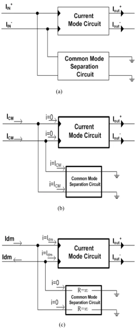
Fig.1c).
matching between current buffers (especially in lower output impedance (in Fig.1-b), needing tight chip area, unbalanced input impedances (in Fig.1-a), topologies are; increased power consumption and as is shown in Fig.1. Some drawbacks of these current buffers were used to subtract input signals were reported in 7]. In these topologies multiple Three fully differential current buffer topologies
[2
matching between P type and N type current mirrors differential current buffer 8]. In this approach, [2
mirrors results degraded CMRR and PSRR for fully differential current buffers employing this approach. Although the method used in [7, 29-30] for designing fully differential current buffers was successful in reducing common mode currents, however it produced CMRR which is very sensitive to the transistors parameters.
Due to the increasing importance of fully differential structures, in this work a new common mode separation technique is introduced to design high CMRR fully differential current buffers. In the proposed method, a common mode separation circuit is connected in parallel with CG or CB current buffers input terminals which act in a way that provides a low impedance path to ground for unwanted common mode inputs preventing them to flow through the main current mode circuit. On contrary, this novel circuit has very high input impedance for differential mode inputs thus facilitates these inputs to reach the current buffer output terminals. As in the proposed approach common mode signals are separated from differential mode ones, we call it 'common mode separation technique'. The interesting property of this method is that in the case of common mode signals it provides both a low impedance path to ground and high input impedance through the main body of current buffer. This double action doubly rejects common mode signals. It is worth nothing that unlike some of the previously used methods, the proposed method does not need balanced inputs for proper operation. This feature thus, both
(a)
(b)
(c)
Figure 1. Fully differential current buffer topologies using single input-single output current buffers [27]
differential mode input signals from unwanted proposed idea is shown in Fig. 2a. To separate
Separation Circuit Conceptual schematic of the
2.1. Implementation of Common Mode
CURRENT BUFFERS
2. PROPOSED FULLY DIFFERENTIAL
finally section V concludes this paper.
Simulation results are presented in section IV and III includes the proposed high current gain stage. based on CG and CB stages are presented. Section described and two fully differential current buffers In section II basic concept of the proposed idea is
mode circuit in parallel. In the case of common separation circuit is connected to inputs of current common mode ones, the proposed common mode
October 2011 impedance path to ground for common mode
currents. But in the case of differential mode inputs common mode separation circuit provides a high input impedance and differential mode input currents are directly conducted to the output of the main current mode circuit as is shown in Fig. 2c. Common mode separation circuit can be implemented using either CMOS or BJT transistors. It can also be applied to both CG and CB stages as will be shown next in this section.
Implementation of common mode separation circuit in CMOS technology is shown in Fig. 3 which can be implemented in BIPOLAR technology in the same way. It consists of M1-M2differential pair, M5
level shifter and M3-M4NMOS transistors. Voltage
at the source node of differential pair, i.e. K node, plays an important role in the operation of the proposed common mode separation circuit. In the case of differential mode inputs, voltage at node K will be at virtual ground due to the M1-M2
differential pair action. This will make M3-M4
NMOS transistors gate voltages, i.e. KK node, at virtual ground (via M5 level shifter) and their
differential mode drain currents equal to zero. Since source nodes of M3-M4transistors are connected to
VSS, the gate-source small signal voltages of those
transistors become zero too. As the result, a high impedance (equal to the output impedance of M3
-M4 transistors i.e. ro3,4) path is provided for
differential mode currents which allows only a negligible portion of differential mode input currents to be drown by common mode separation circuit, leaving ideally the whole differential input currents to get the output terminals of current buffer.
In the case of common mode inputs, voltage at node K will be roughly equal to input nodes
(a)
(b)
(c)
Figure 2. Conceptual schematic of the proposed idea a) basic form b) in common mode configuration c) in differential mode configuration
IJE Transactions B: Applications Vol. 24, No. 3, -240
voltage (and node KK voltage) implies that
gate-3 4 3
currents in which gm , is transconductance of M
-3 4
1/gm
impedance path of , for common mode connected transistors providing a low input
3 4
to zero. Hence M -M transistors act as diode
3 4
drain voltage of M -M NMOS transistors is equal Equality of input terminals voltages with node K
1 2
voltage tracking action of M -M differential pair.
A B K
voltages i.e. V =V =V . This is mainly due to the
3 4
4
input common mode currents to ground, allowing ideally, zero common mode current to get the output terminal of current buffer.
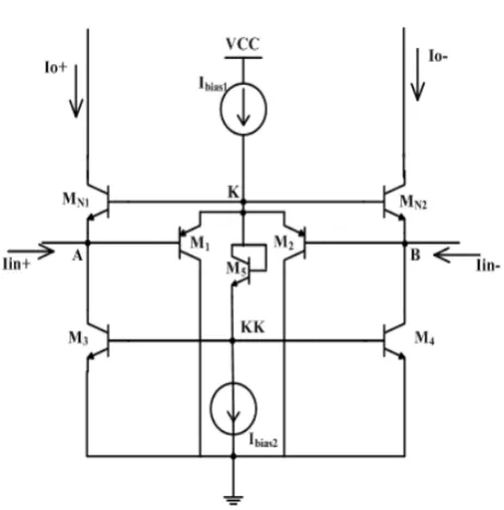
In Figures 5 and 6 the proposed common mode separation circuit is applied to CG and CB stages respectively to separate differential mode currents from unwanted common mode ones in order to design a fully differential current buffer.
2.2. Fully Differential Current Buffer Design Based on Common Mode Separation Technique
Fig. 4 shows two CG stages which were conventionally used to process differential signals. In this configuration MN1-MN2 are common gate
transistors biased through Ibias current sources and
MB transistor. Current mirrors Mm1-Mm2 and M'm1
-M'm2 transfer the input signals to the loads. In this
configuration, both unwanted common mode currents and differential mode ones are transferred to the loads resulting in a CMRR of zero dB for the current buffer of Fig. 4.
The proposed fully differential current buffer is shown in Fig. 5. It is constructed by adding the proposed common mode separation circuit of Fig. 3 to the inputs of conventional current buffer of Fig. 4. It utilizes MN1-MN2 CG stages and common
mode separation circuit implemented with M1-M5
transistors. Favorably M3-M4 transistors of the
common mode separation circuit are also used to bias MN1-MN2 transistors. The gate nodes of MN1
-MN2 are connected to K node of the common mode
separation circuit. Interestingly the proposed fully differential current buffer of Fig. 5 has only three more transistors compared to conventional one of Fig. 4.
It is convinent to expalin the operation of the proposed fully differential current buffer of Fig. 5 by defining input signals (Iin+and Iin-) in terms of
their common mode and differential mode componenets as:
) )
)
In the case of common mode inputs where Iin+=Iinˉ=Ic, the input terminals' voltages are
equally propotional to input common mode currents, i.e. VA=VB=αIc. Due to voltage tracking
action of M1-M2differential pair, voltge at node K
will be rougly equal to the input terminals voltages i.e. VK=VA=VB. This implies a zero gate-source
voltage for MN1-MN2 transistors in common gate
stages. As expalined earlier, in the case of common mode inputs, M3-M4 gate-drain voltages are also
equal to zero turning these transistors to diode connected ones which provide a low impedance Figure 3. Implementation of common mode
separation circuit in CMOS technology
2
+
-Iin +-Iin
Where:
2 Id
-Iin - +Ic (2
2 Id +
Ic= (3) Id = Iin − Iin (4
Iin = +I (1 =
) (5
C N1,N2
3.4 N
1
1
gm
.
ro
A
[(1
a
)
gm
]
: current buffer of Fig. 4 can be found from
IJE Transactions B: Applications Vol. 24, No. 3, October 2011 -242
where, gmN1,N2 and roN are transconductance and
output resistance of MN1-MN2 transistors
respectively and "a" is common mode voltage gain between input terminals (i.e. A and B) and node K which can be represented as:
) .(
. 2 1
) .(
2
2 1
2 1
Ibias Ibias
P
Ibias Ibias
P
R R
gm
R R
gm a
(5-1)
In which, gmp is M1-M2 transistors
transconductances, RIbias1 and RIbias2 are equivalent
output resistances of Ibias1 and Ibias2 current sources
respectively.
In the case of differential mode inputs (Iin+=-Iin
-=0.5Id), M1-M2differential pair makes node K to be
at virtual ground. As is explained before for Fig. 3, M3-M4transistors show high impedance of ro3,4for
differential mode input signals. Hence a negligible portion of differential mode input currents will flow into M3-M4transistors via ro3,4. On the other hand,
gate terminal of MN1 and MN2 transistors will be at
virtual ground while their source nodes are at VB
and VA respectively making gate-source voltage of
MN1 and MN2 equal to –VB and –VA respectively.
As a result MN1-MN2 will performe as simple CG
stages providing low impedance paths of 1/gmN1,N2
to outputs (in which gmN1,N2are transconductances
of MN1-MN2 transistors) for differential mode input
signals. Differential mode gain of the proposed buffer can thus be found from:
current buffer
CMOS technology
BIPOLAR technology 4.
Figure Conventional fully differential CG based
5
Figure . Proposed fully differential current buffer in
6.
4 , 3 2 , 1 4 , 3 2 , 1 . 1 . ro gm ro gm A N N N N
D (6)
Using (5) and (6), the resulted CMRR for the proposed current buffer will be as:
) . 1 ]( 1 ) . 1 .( ) 1 [( ) . 1 .( . 4 , 3 2 , 1 2 , 1 4 , 3 2 , 1 2 , 1 4 , 3 4 , 3 2 , 1 ro gm ro gm gm a ro gm ro gm A A CMRR N N N N N N N N N N C D (7)
Assuming, a≈1 and gmN1,2.ro3,4>>1 simplifies
CMRR as: 4 , 3 2 , 1 .gm
ro
CMRR N N (8)
Fig. 6 shows the BJT version of the fully differential CB stage implemented with common mode separation technique. In this structure, MN1
-MN2 along with M3-M4 transistors forms the
common base stages and the proposed common mode separation circuit is formed with M3-M4
NMOS transistors, M1-M2 differential pair and M5
level shifter. The operation of this circuit is the same as its CMOS counterpart. Note that for simplicity, load current mirrors are not shown.
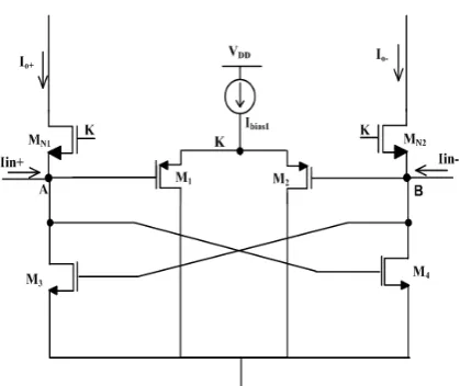
2.3. Common Mode Separation Technique in Partial Positive Feedback Configuration The
proposed common mode separation technique can be arranged in a partial positive feedback configuration to provide a high differential current gain and higher CMRR and PSRR. This configuration in CMOS technology is shown in Fig. 7. As is shown in Fig.7, in this structure, the gates of M3-M4 NMOS transistors in common mode
separation circuit are directly connected to the input nodes (instead of node KK in Fig.3) and gates of common gate NMOS transistors (MN1-MN2) are
connected to the source node of differential pair (M1-M2) i.e. K node. For simplicity, PMOS current
mirrors and loads are not shown.
In the case of common mode inputs, both input nodes have equal voltage i.e. VA=VB=VC, so the
drain-gate terminals of M3-M4 NMOS transistors
are short circuited and hence these transistors act as diode connected transistors providing a low impedance path to ground for common mode signals. Meanwhile, voltage of node K is approximately equal to the input node's voltages
because of the voltage tracking action of differential pair (M1-M2) in common mode separation circuit.
So the gate-source of MN1-MN2 transistors will be
zero and negligible common mode current will flow into these transistors through their output impedances.
interesting operation in the case of differential mode inputs. In this mode, gates of MN1-MN2 transistors
become virtual grounded (because these nodes are directly connected to the source of M1-M2
differential pair which is at virtual ground in differential mode) so these transistors will act as simple common gate stages with input resistance of 1/gmN1,N2 but M3-M4 NMOS transistors establish a
partial positive feedback loop which can be used to produce both high gain and high CMRR. It can be proved that the differential mode current gain due to partial positive feedback can be found from:
1 ) ( 1 2 , 1 4 , 3 2 , 1 4 , 3 N N N N gm gm gm gm
Aid (9)
As stated in [31-32], by proper choosing of η so
that 0<η<1, a high gain and stable current input stage can be obtained. Using (9) the CMRR of the proposed circuit of Fig.7 becomes as:
1 . . 3,4 2 , 1 gm
ro
CMRR N N (10)
As can be seen from (10), structure of Fig.7 has higher CMRR compared to proposed current buffers.
3. SIMULATION RESULTS
IJE Transactions B: Applications Vol. 24, No. 3, October 2011 -244
Table 2. Those are so chosen to get the best possible and reliable results following relations (5) through (10). As in the case of Fig. 5, output currents of the proposed circuits in Figs. 6 and 7 are transferred to the loads using simple current mirrors. In the CMOS based structures, used aspect ratios in all current mirrors and current sources are 50µm/0.5µm. The used load in the simulations is a 1kΩ resistor parallel with 1pF capacitor. In practice, the CB block is mostly used in current mode processing where the impedance of the output node is so low that acts dominantly resistive.
VDD (V)
VCC (V)
Ibias1 (µA)
Ibias2 (µA) Current Buffer of Fig.5 1.4 - 10 5 Current Buffer of Fig.6 - 1.6 50 5 high gain stage of Fig.7 1.4 - 10
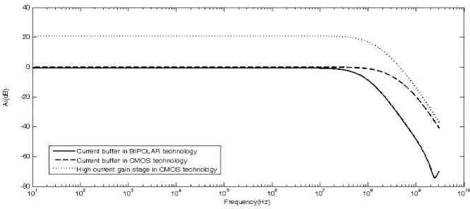
-Current gain (Ai) frequency performance of the proposed structures are shown in Fig. 8 which show current gains of -0.2dB and -0.53dB for the proposed current buffers of Fig.5 and Fig.6, respectively. This implies that common mode separation circuit takes a negligible portion of differential mode currents causing its large portion to be flown through CB and CG stages. Proposed common mode separation circuit has also successful operation in partial positive feedback configuration which results a current gain of 20.86dB for the proposed current gain stage of Fig. 7. The -3dB frequencies are 144MHz and 49.7MHz for the proposed CMOS based and BJT based current buffers, respectively. High current gain stage has also a high -3dB frequency of 80.3MHz.
Fig. 9 shows CMRR frequency performance of the proposed structures. It proves successful operation of the proposed common mode separation technique in alleviating common mode inputs. The resulted CMRR are 32.9dB, 33.1dB and 53.91dB for the CMOS based current buffer of Fig. 5, BJT based current buffer of Fig.6 and CMOS based current gain stage of Fig. 7, respectively. The frequencies at which CMRR approaches 0dB are 675MHz, 385MHz and 3700MHz for the CMOS based current buffer of Fig. 5, BJT based current buffer of Fig. 6 and current gain stage of Fig. 7, respectively. These results prove the great strength of the proposed common mode separation technique in eliminating high frequency unwanted common mode signals.
Stability of the proposed current gain stage is investigated by applying a step input with amplitude of ±1µA. The resulted outputs are shown in Fig. 10 which prove its sufficient stability.
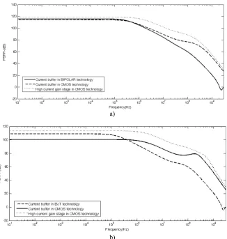
To examine the ability of the proposed circuits in rejecting supply and ground coupled noises, their PSRR performance are also investigated. Results are shown in Fig. 11 which show high PSRR for the proposed structures.
Simulation results are summarized in Table 3. The reported power dissipation also includes the bias circuitry that consists simple (two transistors) current sources and consumes very few power. Corner case simulation results are also studied and
performance for the proposed current buffers. 7.
current input stage
3 4
M -M 20/0.5
1 2
M -M 4.5/0.5
1 2
N N
M -M 30/0.5
stage of Fig. 7 High current gain
1 2 N - N
M M5 10/0.5
M 10/0.5
3 4
M -M 45/0.5
1 2
M -M 3.5/0.5
Fig. 5
Current Buffer of
Transistor W(µm)/L(µm)
TABLE 2. Transistors aspect ratios TABLE1. Used bias currents and voltages
Figure
Figure 9. CMRR frequency performance of proposed structures
Figure
Figure 8. Ai frequency performance of proposed structures
. CMRR frequency performance of proposed structures
a)
b)
Figure 11.PSRR frequency performance of proposed structures a)PSRR- b)PSRR+
TABLE 3. Proposed Current Buffers (CB) and high current gain stage specifications Proposed current buffer High
Current Gain Stage In CMOS In Bipolar
Ad(dB) -0.2 -0.54 20.86
f-3dB (MHz) 144 49.7 80.3
CMRR(dB) 32.9 33.1 53.91
fTof CMRR (at which CMRR=0dB) 675MHz 385Mhz 3700MHz
PSRR-(dB) 114 116 118.85
PSRR+(dB) 100 109 113.50
PD(µW) 179 379 305
Simulation results of the proposed current buffers are compared with other related works in Table 5. As can be seen, the proposed current buffers offer low voltage operation compared to others. The BJT version of the proposed current buffer also has very low power consumption compared to other BJT based current buffers while that of CMOS version is much less than other CMOS types and comparable with that of the best one (to be notified that the consumed power reported for [29] excludes the power of bias circuitry which is some tens micro watts).
4. CONCLUSION
This paper proposes a novel method to design fully differential current buffers. In the proposed method, common mode currents are conducted to ground while differential mode ones are forwarded to the output loads. It is thus called Common Mode Separation technique. The proposed technique combined with partial positive feedback is used to design low power and low voltage high gain current input stages.
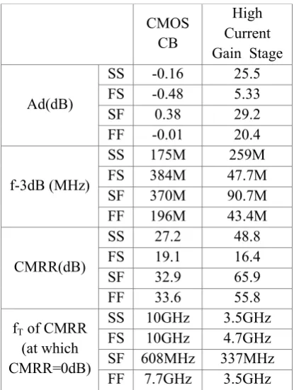
TABLE 4. Corner case simulation results of the proposed Current Buffre(CMOS) and high current gain stage specifications
CMOS CB
High Current Gain Stage
Ad(dB)
SS -0.16 25.5 FS -0.48 5.33
SF 0.38 29.2
FF -0.01 20.4
f-3dB (MHz)
SS 175M 259M
FS 384M 47.7M
SF 370M 90.7M
FF 196M 43.4M
CMRR(dB)
SS 27.2 48.8
FS 19.1 16.4
SF 32.9 65.9
FF 33.6 55.8
fTof CMRR
(at which CMRR=0dB)
SS 10GHz 3.5GHz FS 10GHz 4.7GHz SF 608MHz 337MHz FF 7.7GHz 3.5GHz
TABLE 5. Comparison of the proposed current buffers with other related works
Refs. Technolog y
Ad
CMRR Supply Voltage
Power
dissipation Year Value
(dB)
f-3dB (MHz)
[22] BJT -12dB NA 52dB NA NA 1990
[23] CMOS -6.02dB >37MHz 38dB 5V 22mW 1998
[26] BJT 66mdB 831MHz 55dB ±1.5V 6.7mW 2010
[27] CMOS NA 57MHz 50dB ±1.5V NA 2009
[28] CMOS 6dB 1.25MHz 62dB 5V 3mW 1991
[29] CMOS 0.1dB 369MHz 98dB ±0.75V 0.135mW 2010
proposed CMOS
0.172d
B 144MHz 32.9 1.4V 0.179mW 2011
Based on the proposed method, two fully differential current buffers and a high gain current input stage are introduced and simulated presenting a sufficiently high CMRR and PSRR. Simplicity is another important characteristic of the proposed method. There is no need to concern about stability conditions in the proposed structures. Compared to conventional current buffers, the proposed one has only three more transistors while offering high CMRR and true fully differential operation. This technique is at the beginning of its life and is gifted much more capabilities to be opened and improved by further attentions of interested researchers.
5. REFERENCES
Amp-Based Current-Mode Instrumentation Amplifiers (CMIA)", IEEE Transaction on Instrumentation and Measurement,
Gain Current Amplifier", Analog Integrated Circuits and Signal Processing,
Swing Current Mode BICMOS Logical Operators",
International Journal of engineering Transactions A: Basics,
performance operational transconductance amplifier and its application in a tunable Gm-C filter", Microelectronics Journal,
Rodríguez-Vázquez A. "A 2.5MHz 55dB Switched-Current BandPass SD Modulator for AM Signal Conversion" Proceedings of the 23th European Conference on Solid
Selective Circuits", Electronics Letters, Vol. 25, (1989),
Fully Differential Current Buffer and Its Application as a Voltage Amplifier", International Conference on Modeling,
"Wideband CMOS transimpedance amplifier" Electronics letters,
Analysis and Design" IEEE Transactions on Circuits and Systems-I: Regular Papers,
Mode All pass and Notch Filter Employing Single Current Follower" 14th International Conference on Mixed Design
"Simulation of Chua’s Chaotic Oscillator Using Unity-Gain Cells", 7th International Caribbean Conference on
Amplifier (COA): CMOS Realization and Active Compensation", Analog Integrated Circuits and Signal Processing,
Mode Operational Amplifier and Its Use for Band-Pass Filter Realization", International Conference on Applied
Generation Current Conveyor", ETRI Journal, Vol. 28,
9th Order Linear Phase Baseband Switched Capacitor Filter", International Journal of engineering, Transactions A: Basics,
Linearity Continuous Time Filter in 5-V VLSI CMOS”,
R.G., “Analysis and Design of Analog Integrated Circuits”, 5th Edition, John Wiley, 2009.
Current Mode Transimpedance Preamplifier", The 11th IEEE International Symposium on Electron Devices for Microwave and Optoelectronic Applications, (2003),
Operational Amplifier Using Level Shifter Technique", International Symposium on VLSI Design, Automation
current mode operational amplifier with improved input– output impedances and its filter applications"
International Journal of Electronics and
Communication,
Conveyor based Buffer for High Bandwidth, Low Signal Applications", Proceedings of The 6th IEEE International Conference on Electronics, Circuits and Systems, Vol. 2, (1999), 903-906.
Simulation and Control, ICMSC, (2010), 30-34. 759-761.
State Circuits, IEEE, (1997), 156-159. Vol. 42, No. 6, (2011), 827-836. Vol. 20, No. 3, (2007), 211-220.
(2008), 239 – 244. and Test, (2006), 1-4.
128-132.
IEEE J. Solid-State Circuits,Vol. 27, (1992), 1270-1276
Vol. 58, NO.3, (2009), 563-569.
Vol.41, (2004), 147–157.
Vol. 39, (2003), 587-588.
Vol. 53, (2006), 26-39.
Devices, Circuits and Systems, IEEE, (2008), 1-4.
Vol. 24, (2000), 141-152.
Electronics, (2006), 3-6.
No. 4, (2006), 495-501.
Vol. 17, No. 1, (2004), 19-24. of Integrated Circuits and Systems, IEEE, (2007), 638-640
22. Payne, A., Toumazou, C. and Ryan, P., "Differential Current
23. de la Rosa, J.M., Perez-Verdu, B., Medeiro, F.,
Dominguez-24. Tauro, A., Marzocca, C., Francesco, C.T., Giandomenico,
Circuits and Systems, Vol. 1, (2003), 288-291.
Microelectronics Journal,Vol. 29, (1998),
Vol. 26, (1990), 1718-1719.
10th IEEE International Conference on Electronics, Voltage Feedback CMOS Amplifiers", Proceedings of Di., "Common Mode Stability in Fully Differential
817-820.
Circuits", Fully Differential Current Mode Buffer for HF SI Castro, R. and Rodriguez-Vazquez, A., "A CMOS 0.8µm
Letters,
Electronics
Input Cell with Common Mode Feedback",
25. Duque-Carrillo, J.F., “Control of common-mode component 13. Altun M. and Kuntman H., "A Wideband CMOS Current-11. Sanchez-Lopez C., Trejo-Guerra R., Tlelo-Cuautle E.,
14. Soliman A.M., "New Fully Differential CMOS Second
15. Hashemipour, O. and Goravanchi, P., "A Very Low Voltage
16. Durham, A.M, Redman-White, W. and Hughes, J.B.,
“High-17. Gray, P. R., Pual, J. Hurst., Stephen, H. Lewis. and Meyer,
19. Heng, S. and Pham, C.K., "A 1.5V Current-Mode
20. Altun, M. and Kuntman, H., "Design of a fully differential
21. Alves, L.N. and Aguiar, R.L., "A Differential Current 18. Tao, R. and Berroth, M., "Wide-band Low-Power CMOS
9. Yuan F., " Low-Voltage CMOS Current-Mode Preamplifier:
10. Ergun E. and Ulutas M., "Low Input Impedance Current– 3. Delavar, A.G., Navi K. and Hashemipour O., "High Speed Full 2. Lima, J.A. de, "A Low-Voltage Wide-Swing Programmable-1. Azhari, S. J. and Fazlalipoor, H., "CMRR in
Voltage-Op-4. Rezaei, F. and Azhari, S. J., "Ultra low voltage, high
5. de la Rosa J.M. , Pérez-Verdú B., Medeiro F., and
6. Roberts G.W. and Sedra A.S., "All Current Mode Frequency
7. Safari, L. and Azhari, S. J., "A New Low Voltage Low Power
8. Kossel, M., Menolfi, C., Morf, T., Schmatz, M. and Toifl, T.,
12. Awad Inas A. and Soliman A. M., "Current Operational
Symposium on Circuits and Systems, IEEE, (2009),
CMOS Current-Mode Amplifiers and Filters", International Symposium on Circuits and Systems, IEEE,
differential Current Buffer” IEICE Electronics Express,
differential current buffer with ultra low input impedance, high CMRR, low power and low voltage", 3rd
Analog Integrated Circuits and Signal Processing,
Carrillo, J.F., "1-v Rail-to-Rail CMOS Opamp with Improved Bulk-Driven Input Stage", IEEE Journal of Solid State Circuits,
3127, HFA 3128, Data sheet, www 1381-1384.
(1991), 781-784.
Vol. 7, No. 11, (2010), 765–771.
International Conference on (2011), 229-233.
Vol.42, No.3, (2007), 508-517. 31. Wang, R. and Harjani, R., “Partial Positive Feedback for 30. Azhari, S.J., Ghorbani, A., Safari, L., " A novel fully
29. Azhari, S. J. and safari, L., “A high CMRR low power fully 28. Zele, R. H., Allstot, D.J. and Fiez, T.S., "Fully-Differential
32. Carrillo, J.M., Torelli, G., Perez-Aloe, R. and
Duque-33. Intersil, Transistor arrays HFA 3046, HFA 3096, HFA Gain Enhancement of Low Power CMOS OTAs",
Analog Integrated Circuits and Signal Processing,
in CMOS continuous-time fully differential signal processing,”
OCB: An Innovative Block with Extremely Low Input Impedance and High CMRR", Proceeding of world academy of science, engineering and technology, Vol. 61,
Differential Current Followers/Amplifiers", International Vol. 4, (1993), 131-140.
(2010), ISSN 2070-3724 part 1-114-125.
27. Alzaher, H. and Tasadduq, N., "Realizations of CMOS Fully 26. Azhari, S. J. and Safari, L., "The Orderly Current Buffer,
![Figure 1. Fully differential current buffer topologies using single input-single output current buffers [27]](https://thumb-us.123doks.com/thumbv2/123dok_us/238852.2018564/3.595.319.529.103.651/figure-fully-differential-current-buffer-topologies-current-buffers.webp)