Output-Conductance Transition-Free Method for Improving
Radio-Frequency Linearity of SOI MOSFET Circuits
A. Daghighi*
Abstract: In this article, a novel concept is introduced to improve the Radio Frequency (RF) linearity of Partially-Depleted (PD) Silicon-On-Insulator (SOI) MOSFET circuits. The transition due to the non-zero body resistance (RBody) in output conductance of PD SOI devices leads to linearity degradation. A relation for RBody is defined to eliminate the transition and a method to obtain transition-free circuit is shown. 3-D Simulations of various body-contacted devices are carried out to extract the transition-free body resistances. To identify the output conductance transition-free concept and its application to RF circuits, a 2.4 GHz Low Noise Amplifier (LNA) is analyzed. Mixed mode device-circuit analysis is carried out to simultaneously solve device carrier transport equations and circuit spice models. FFT calculations are performed on the output signal to compute harmonic distortion figures. Comparing the conventional body-contacted and transition-free SOI LNAs, third Harmonic Distortion (HD3) and Total Harmonic Distortion (THD) are improved by 16% and 24%, respectively. Two-tone test is used to analyze third order intermodulation distortions. OIP3 is improved in transition-free SOI LNA by 17% comparing with the conventional body-contacted SOI LNA. These results show the possibility of application of transition-free design concept to improve linearity of RF SOI MOSFET circuits.
Keywords: Body-Contact, Linearity, Output-Conductance, MOSFET, Silicon-on-Insulator.
1 Introduction1
Silicon-on-Insulator MOSFETs are commonly utilized for digital, RF and analog applications. Since the active silicon film layer is electrically insulated, floating body effects (FBE) are normally observed in partially-depleted SOI MOSFETs [1]. The kink which is associated with FBEs is frequency dependent and vanishes at RF operating range. However, there is a need to connect the device body to an external voltage for RF applications [2-4]. Body-Contacted devices are required to avoid body voltage variations and to obtain proper device matching. Therefore body-ties are used to suppress FBEs and the resultant fluctuations.
Several body contact structures are proposed to control the body voltage. H-gate (or T-gate) structure is used to connect the body of the device to an external contact [5]. In the H-gate device, the body voltage is only considered to vary along the device width. Due to the parallel connection of the P+ doped body contacts in a multi-finger device layout, bias-dependent body resistance modeling, hence the body voltage
Iranian Journal of Electrical & Electronic Engineering, 2013. Paper first received 20 Feb. 2013 and in revised form 6 May 2013. * The Author is with the Department of Electrical Engineering, Faculty of Engineering, Shahrekord University, Shahrekord, Iran. E-mail: [email protected]
computation is straightforward [6]. Therefore a uniform body voltage along various fingers is obtained. However, the extra capacitance of gate extension degrades the device cut-off frequency. I-gate body-tied SOI structure uses a strip of p- silicon at the center of the transistor to connect the device body to an external contact [7]. The total gate capacitance is smaller than the H-gate structure hence improved high frequency performance is achieved. However, a non-uniform body voltage along various fingers can be obtained in a large multi-finger device layout as a result of P- strip resistance. The elevated body voltage at the middle fingers reduces the device total gate capacitance and improves the high frequency performance at the cost of degradation of device matching.
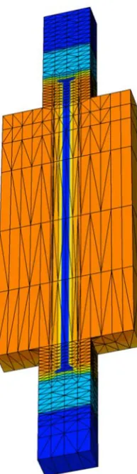
Three-dimensional (3-D) structure of an H-gate SOI device is shown in Fig. 1. The traveling holes in the impact ionization process accumulate in the body and passes under the gate extension to escape to the P+ doped body contact. As a result, body voltage increases in the center of the device furthest away from the body contact. Body voltage variations alongside the device width are included in the body resistance model to compute device terminal characteristics. As the technology moves into the nano-scale channel length dimensions, the body resistance increases due to the
Fig. 1 3-D structure of an H-gate body-contacted PD SOI MOSFET.
extreme narrowing of the neutral body strip. The gate and source/drain depletion regions make the body resistance (RBody) highly bias-dependent. In addition to the impact of device electrostatics on the body resistance, RBody differs between various layout implementations of a transistor. The number of fingers and finger widths directly influences the body resistance. This is significant considering the body resistance as a design parameter.
Output conductance (gds) variations directly affect the device intrinsic gain and degrade the transistor linearity. Several gds transitions versus frequency for PD SOI MOSFET are reported [8]. The transition due to the non-zero RBody occurs in the radio frequency range and affects the linear behavior of RF circuits, for example, increases Total Harmonic Distortion (THD) and lowers third order intercept points (IIP3). Therefore, it is required to choose the device body resistance to eliminate the transition and obtain transition-free devices/circuits while maintaining a proper contact to the body [9, 10].
In this paper, we propose a method to eliminate the transition in output conductance of SOI MOSFETs. Then, a transition-free design procedure is explained to improve the radio frequency linearity. The procedure is tested on low noise amplifier and improved linearity performance is achieved. The paper is organized as follows: Device structure and simulation model are explained in section 2, the transition-free concept is introduced in section 3, low noise amplifier
transition-free design procedure is discussed in section 4, followed by a conclusion in section 5.
2 Device Structure and Simulation Model
Body resistance value can be a circuit design parameter that is adjusted during the layout implementation by varying the number of fingers. Zero-bias body resistance is approximately given by:
(
S D)
F bsh
F ext Body
X
X
L
N
W
R
N
R
R
−
−
⋅
⋅
+
=
20 (1)
where NF denotes the device number of fingers, Rext includes the P- doped extension resistance, Rbsh is the zero-bias body sheet resistance, XS/D is the source/drain to body depletion width, W defines device width and L is the channel length. Eq. (1) is derived based on the assumption that the mobile charges in the neutral body region form a rectangular shape. While Eq. (1) computes the zero-bias body resistance and is derived based on the geometry of the mobile charges, it does not include the effect of gate/drain/source biasing and the impact of body voltage variations along the device width on the geometry of mobile charges. Therefore, 3-D device simulations are required to fully capture the body resistance variables. For this reason, the structure shown in Fig. 1 is considered. The PD SOI MOSFET parameters are as follows: L=45 nm, W=1 μm, TBox=100 nm, TSi= 75 nm, Tox=1.5 nm, Body doping NA=3×1018 cm-3 with 45° tilt angle HALO implants, Source/Drain as Gaussian profiles with the peak concentration of ND=9×1019 cm-3. The substrate is considered at 0 V and thermal contact at 300 K. Models accounting for carrier mobility dependence on doping level, lattice temperature and band gap narrowing; Shockley-Reed-Hall recombination with concentration dependent life times; Auger recombination and temperature dependent saturation velocities and impact ionization coefficients were included.
Fig. 2 shows 3-D view of the active silicon film layer including body, P- doped extension, P+ doped body contact and drain/source regions. The STI oxides are not shown. MESH routine is used to define the refinements and generate the grid point densities [11]. The number of grid points shows the simulation complexity and the refinements required to fully capture the device physics. Extra refinement is introduced in the P- extension where it is connected to the N+ source and drain regions. 3-D simulation complexity increases further as the number of fingers in the device structure increases. Self-heating effects are pronounced in SOI devices as a result of low thermal conductivity of BOX layer. Therefore, non-isothermal modified drift-diffusion model is used to solve carrier transport equations [12]. Thus, additional 3-D simulation time is required to capture thermal effects in active silicon films in addition to device electrostatics.
Fig. 2 3-D view of the active silicon film layer, L=45 nm.
3 Simulation Results
Five device structures are simulated: A floating body device and H-gate device structures with NF=1, 2, 3 and 6. Non-isothermal drift-diffusion approach is used to analyze the structures. Fig. 3 shows IDS versus VDS for the simulated devices. Floating body device shows the current kink near VDS=0.75 V. The kink is eliminated in the output characteristic as the body is contacted to the ground potential.
Fig. 3 Drain-source current vs. Drain-source voltage at VGS=1.2 V.
Fig. 4 Output Conductance vs. Frequency at VGS=VDS=1.2 V.
However, there is a gradual increase of drain current for the device with NF=1 as a result of elevated body voltage which lowers the threshold voltage, hence, current drive increases beyond VDS=0.8 V. As the number of fingers increases, the body resistance decreases (NF=2 and NF=3). Thus, body voltage is lowest in device with NF=6. Therefore, current drive is slightly higher in the device with NF=2 and the difference gets smaller as the number of fingers increases beyond that.
AC simulation is based on small-signal analysis which solves the device as small sinusoidal signals are superimposed on DC operating point. The steady-state solution is saved at VGS=VDS=1.2 V and recovered later for ac analysis. The admittance matrix which is essentially the current response at a given node to a small voltage signal at another node is computed at various frequencies. The output conductance is then extracted from the admittance matrix:
(
)
(
Y D D)
gds =Re , (2) The output conductance versus frequency is shown in Fig. 4. The transitions due to self-heating effects are seen in all the graphs. The floating body device shows a descending transition at frequencies higher than 2×10⁸ Hz. The transition repeats in the H-gate structure with NF=1.
Fig. 5 Transition-free body resistances at various biasing points.
Fig. 6 Small-signal model of PD SOI MOSFET.
This is due to the occurrence of pole-zero doublets in the output conductance frequency response [8]. The transition is eliminated in the structure with NF=2. In this structure, the body resistance is adjusted such that the output conductance transition-free device is obtained. Therefore, adjusting RBody influences the non-zero body resistance transition. The descending transitions in the first and second devices alter to ascending action in NF=3 and 6 structures and moves to higher frequencies due to the dependence of pole-zero doublet frequencies to the body resistance value. While largest number of fingers makes the body resistance smallest and the best body voltage control is obtained, it introduces a large transition in the output conductance at RF frequencies.
The transition translates to characteristic nonlinearity and it disappears in transition-free biasing points (VGS=VDS=1.2 V, NF=2) where the body resistance is properly adjusted. Therefore, for every biasing point, a body resistance to obtain transition-free device is required. Fig. 5 shows the transition-free body resistances simulated at various biasing points. The number of fingers is varied such that the transition-free operating regime is ensured. The biasing points are chosen in the device saturation region. As the gate voltage increases, a device with large number of fingers is required to remain in the transition-free condition. Therefore, Fig. 5 can be used as a look-up table to adjust the number of fingers of a device in a circuit to work in transition-free operating regime.
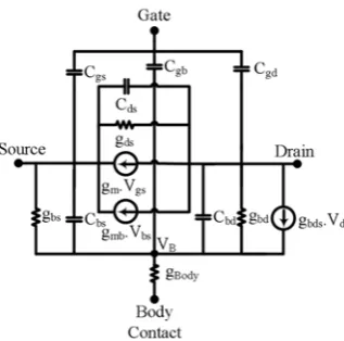
In order to develop the concept analytically, the small signal model of Fig. 6 is considered where the gate and source are tied together.
The conductance of body node to the body contact terminal is shown by gBody. The body contact is grounded. The small signal model from drain to gate/source is divided to Low Frequency (LF) and High Frequency (HF) sub-circuits.
Fig. 7 shows the LF and HF sub-circuits where the gate and source are connected to the ground. Using the LF and HF sub-circuit, the body node voltages are computed:
Fig. 7 Low and High frequency sub-circuits seen from the drain terminal, VGS=0.
( ) (
)
bd bs Body D bd bds B g g g V g g LF V + + += (3)
( )
bd bg bs D bd B C C C V C HF V + += (4)
In order to eliminate the transition of output conductance and to obtain transition-free devices, the body node voltage at low and high frequencies are set equal and the body resistance is computed as:
( )
(
)
(
)
bd bs bg bs bd bd bg bs bds bd Body Body C g C C g C C C g C g R − + + + + == −1
(5) The result of Eq. (5) is used to compute the body resistance for which the transition-free device is obtained and it relates the small signal model parameters to the body resistance. Eq. (5) is essentially an analytical variant of Fig. 5 for body resistance computation.
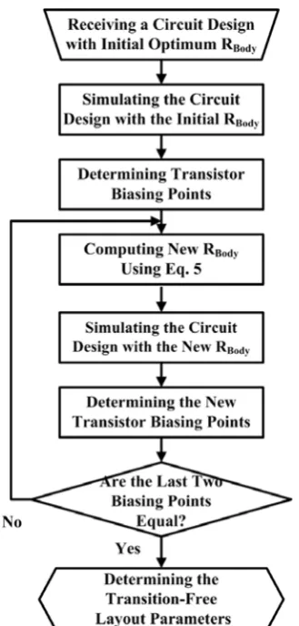
An example of a method for determining and storing circuit layout parameters for SOI MOSFET circuits to improve their radio frequency linearity is illustrated in Fig. 8. Initially, a circuit design including one or more SOI MOSFETs where each transistor has a respective first RBody is received. The received circuit design is then simulated with the one or more SOI MOSFETs. Following simulation, the first biasing points of the SOI MOSFET circuit can be determined. Next, a second RBody for each of the one or more SOI MOSFETs is calculated using Eq. (5). The values for the variables are obtained from the simulation of the received circuit design. The received circuit design is then simulated with the second RBody. Following the second simulation, the second biasing points of the SOI MOSFET circuit are determined. Next, the first biasing points and the second biasing points are compared to determine whether they are equal. If the first biasing points and the second biasing points are equal, then it is determined that the second RBody of each of SOI MOSFETs in the circuit is a transition-free RBody that results in an output conductance transition-free circuit, which in turn results in improved radio frequency linearity of the SOI MOSFET circuit. If the first biasing points and the
Fig. 8 Transition-free circuit design procedure.
second biasing points are not equal, then the updated circuit parameters are used to iteratively calculate a subsequent RBody for each of the one or more SOI MOSFETs. In particular, once the RBody of at least one of the SOI MOSFETs in the received circuit is changed to its second RBody, the biasing points of that SOI MOSFET change, which may affect the biasing points of any other SOI MOSFETs in the circuit. As a result, the RBody of each of the SOI MOSFETs in the circuit must be recalculated using Eq. (5). The aforementioned steps are then repeated as many times as necessary until the first biasing points and second biasing points are equal. As a result, output conductance transition-free SOI MOSFETs and, in turn, an SOI MOSFET circuit with improved radio frequency linearity can be obtained.
4 Low Noise Amplifier Case Study
Low noise amplifier is a key component which is located close to the antenna in a generic RF system. Thus, it is required for an LNA to maintain good linearity and add as little as possible distortion to the signal [13]. To identify the output conductance transition-free concept and its application to RF circuits, a 2.4 GHz low noise amplifier is analyzed. Fig. 9 shows the circuit structure. A cascode topology with spiral
Fig. 9 Cascode structure of a 2.4 GHz SOI LNA, Mixed mode device-circuit simulation.
inductor, proper matching and biasing components are chosen. Mixed mode device-circuit analysis is carried out to simultaneously solve carrier transport equations and circuit spice models. The method mentioned in Fig. 8 is used to obtain transition-free circuit.
For this purpose, the transistors' biasing points are computed. The RBody values are extracted from Fig. 5 and calculated according to the biasing points. The circuit is simulated with the new RBody values and corresponding biasing points are computed. The loop repeated for once until the first and second biasing points are equal. Consequently, the RBody values and the number of layout fingers are extracted. For comparison, a conventional body-contacted SOI LNA is simulated such that the numbers of fingers in transistors' layout are implemented to obtain proper body resistance for the near-ideal body voltage control.
Fig. 10 Harmonic distortion figures, Vin=0.1 mV.
Fig. 11 LNA output signal spectrum.
Analysis of harmonic distortion is carried out on the output voltage while a sinusoidal input signal is input to the LNA. FFT calculations are performed on the output signal to compute harmonic distortion figures. Fig. 10 shows the results. As it can be seen, comparing the conventional body-contacted and transition-free SOI LNAs, third harmonic distortion (HD3) and THD are improved by 16% and 24%, respectively. Furthermore, third order voltage intercept point is used for distortion analysis and for small input voltage is defined as [14]:
3 3
HD A
IP = (6)
where A denotes the output signal amplitude. As it is shown in Fig. 10, third order intercept point is improved by 5% for transition-free SOI LNA.
Intermodulation distortion is another result of nonlinear amplification. Two-tone test is used to analyze third order intermodulation distortions (IMD3) where two closely frequency separated sinusoidal signals are applied at the same input port [11].
The output signal spectrum is then calculated and third order intermodulation products at (2f1-f2) and (2f2 -f1) are extracted.
Fig. 11 shows the result of exciting the LNA input with two signal amplitudes f1=2.4 GHz and f2=2.42 GHz. The figure clearly shows the fundamental and
Fig. 12 Output signal power vs. input for fundamental and third order intermodulation products, two-tone test results.
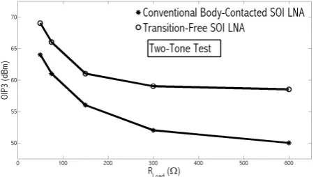
Fig. 13 Third order output intercept point vs. load resistance.
third order intermodulation products. In addition, higher order harmonics and intermodulation products are evident from the output signal spectrum. Fig. 12 shows the output level signal for fundamental and third order intermodulation levels versus input signal power. The third order output intercept point (OIP3) is the output power for which the asymptotes for the response at third order intermodulation product and fundamental cross. As it can be seen, OIP3 is improved in transition-free SOI LNA by 17% comparing with the conventional body-contacted SOI LNA. The load resistance can influence circuit nonlinearity caused by output conductance transition. Therefore, the effect of load resistance on OIP3 is investigated and is shown in Fig. 13. As it can be seen, OIP3 increases by 8% in transition-free SOI LNA at RLoad=50 Ω where the load impedance influences the impact of output-conductance transition the most. The OIP3 difference between transition-free and conventional body-contacted SOI LNA further increases as the load impedance approaches RLoad=600 Ω. These results show the possibility of application of transition-free design concept to improve linearity of RF SOI circuits.
5 Conclusion
We demonstrate a new method to improve linearity of radio frequency SOI MOSFET circuits. Based on the new concept, body resistance is a design parameter that is adjusted to eliminate the transition in the output conductance of PD SOI MOSFETs. Once transition-free device is obtained, the linearity improves. A circuit design procedure explains how to adjust the body resistances to obtain transition-free circuits. The output of the procedure depicts the number of fingers in the layout implementation for each of the transistors in the circuit. Comprehensive distortion analysis of a SOI low noise amplifier demonstrates improvement in distortion figures in comparison with a conventional body-contacted SOI LNA. As a result, output conductance transition-free SOI MOSFETs and, in turn, an SOI MOSFET circuit with improved radio frequency linearity is obtained. The new concept is applicable to all radio frequency PD SOI MOSFET circuits.
References
[1] Colinge J.-P., Silicon-on-insulator technology: materials to VLSI, Kluwer Academic Publishers, 3rd Edition, 2004.
[2] Lee S., Jagannathan B., Narasimha S., Chou A., Zamdmer N., Johnson J., Williams R., Wagner L., Kim J., Plouchart J., Pekarik J., Springer S. and Freeman G., "Record RF Performance of 45-nm SOI CMOS Technology", IEEE International Electron Device Meeting, pp. 255-258, 2007. [3] Fathipour M., Refan M. H. and Ebrahimi S. M.,
“Design of a Resonant Suspended Gate MOSFET with Retrograde Channel Doping”, Iranian Journal of Electrical and Electronic Engineering, Vol. 6, No. 2, pp.77-83, 2010.
[4] Rana A., Chand N. and Kapoor V., “A Novel Hybrid Nano Scale MOSFET Structure for Low Leak Application”, Iranian Journal of Electrical and Electronic Engineering, Vol. 7, No. 2, pp. 112-121, 2011.
[5] Raskin J. P., “Wideband Characterization of SOI Materials and Devices”, Solid-State Electronics, Vol. 51, No. 9, pp. 1161-1171, 2007.
[6] Daghighi A. and Asgari-Khoshoiee A., “A Width-dependent Body Voltage Model to Obtain Body Resistance in PD SOI MOSFET Technology”, 8-th International Conference on Advanced Semiconductor Devices & Microsystems (ASDAM), pp. 45-48, 2010.
[7] Wu C., Yu C., Shichijo H. and Kenneth K. O., “I-Gate Body-Tied Silicon-on-Insulator MOSFETs With Improved High-Frequency Performance”, IEEE Electron Device Letters, Vol. 32, No. 4, pp. 443-445, 2011.
[8] Lederer D., Flandre D. and Raskin J. P., “High Frequency Degradation of Body-Contacted PD SOI MOSFET Output Conductance”, Semiconductor Science and Technology, Vol. 20, No. 5, pp. 469-472, 2005.
[9] Daghighi A. and Pourdavood N., “Method for Improving the Radio Frequency Linearity of Silicon-on-Insulator MOSFET Circuits”, USPTO Patent Publication, US 20120233579 A1, US 8375341 B2.
[10] Pourdavoud N. and Daghighi A., “Impact of Body Resistance on RF Linearity of SOI MOSFET Circuits”, IEEE 4th International Nanoelectronics Conference (INEC), pp. 1-2, 2011.
[11] ISE TCAD Manual. ISE integrated system engineering, Version 10.0; 2004.
[12] Daghighi A., Osman M. A. and Imam M. A., “An Area Efficient Body Contact for Low and High Voltage SOI MOSFET Devices”, Solid-State Electronics, Vol. 52, No. 2, pp. 196–204, 2008. [13] Razavi B., RF Microelectronics, Prentice Hall,
2nd Edition, 2011.
[14] Cerdeira A., Aleman M. A., Estrada M. and Flandre D., “Integral Function Method for Determination of Nonlinear Harmonic Distortion”, Solid-State Electronics, Vol. 48, No. 12, pp. 2225-2234, 2004.
Arash Daghighi received B.Sc. Degree from Isfahan University of Technology in 1994 and Ph.D. degree from Washington State University in 2004 in the area of microelectronics. He later joined Intel Corp., Hillsboro, OR. His research interests include Silicon-on-Insulator microelectronic devices and circuits. He is currently Assistant Professor of Electrical Engineering at Shahrekord University.