www.astesj.com
Special issue on Advancement in Engineering Technology
ISSN:2415-6698
Control of a three-stage medium voltage solid-state transformer
Claudio Busada1, Hector Chiacchiarini1, Sebastian Gomez Jorge*1, Favio Mengatto1, Alejandro Oliva1, Jorge Solsona1, German Bloch2and Angelica Delgadillo2
1Instituto de Investigaciones en Ingenier´ıa El´ectrica (IIIE), Universidad Nacional del Sur (UNS)-CONICET and
Dpto. Ing. El´ectrica y de Computadoras, UNS, Av. Alem 1253, (8000) Bah´ıa Blanca, Argentina.
2ICSA S.A. - Argentina
A R T I C L E I N F O A B S T R A C T
Article history:
Received: 26 October, 2017 Accepted: 17 November, 2017 Online: 07 December, 2017
This paper proposes the modeling and control of a Solid-State Transformer using a three-stage conversion topology. First, a rectification stageisused,whereathree-phase high-voltageACsignal is converted to a DC level; this stage is then followed by a DC-DC converter, and finally an inverter is used to convert the DC into a three-phase low-voltage AC signal. The adopted topology is modeled using a simplified model for each stage, useful to design their controllers.Basedonthesemodels,thecontrollersaretunedtoobtaina good performance to sudden load changes. This performance is tested throughsimulations.
Keywords :
Solid State Transformer Control
Power Electronics
1
Introduction
It is necessary to mention that this paper is an tension of work originally presented in [1]. This ex-tension includes a detailed description of the pro-posed models and controllers. These models are used for tuning the controller parameters in order to ob-tain good performance in presence of sudden load changes.
Solid-State Transformers (SST) are emerging as a new technology capable of replacing power distribu-tion transformers [2]. It is expected that the next generation of the power distribution transformers is based on power electronics semiconductor devices [3]. By using these semiconductors, it is possible to design an apparatus based on power converters with smaller and lighter high-frequency transformers. In this way, it is possible to obtain a smaller and lighter distribu-tion transformer when compared with a tradidistribu-tional transformer of the same power rating. Roughly speak-ing, SSTs work as follows. In a first stage a sinusoidal signal of, typically, 50 or 60 Hz is converted to a high-frequency signal. Then, the amplitude of this signal is changed, by using a small high-frequency trans-former, and finally in a third stage a new signal of the same frequency as the input signal but different amplitude is obtained.
Several topologies for the SST can be found in the literature, with their advantages and disadvantages
[4]. In addition, it is possible to find some reviews dealing with the subject [5, 6]. Applications in trans-portation and smart grid can be found in [7]; whereas a topology based on SiC devices can be found in [8]. Also, a traditional transformer and an SST were com-pared in [9], and a procedure to obtain a detailed model of an SST topology can be found in [10].
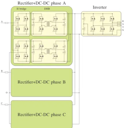
Figure 1:SST topology.
A three-stage SST is considered in this paper [7]. Its topology is shown in Figure 1. The three stages are: a rectification stage, where a three-phase high voltage (HV) AC grid voltage is converted to a DC signal, a DC-DC converter stage (multiple stages in parallel) that provides isolation and performs the level adap-tation, and finally, an inverter stage that converts the DC signal into a three-phase low voltage (LV) AC si-nusoidal wave.
In this paper, simple models for each stage are pro-posed. Using these models, the required controllers are designed and their parameters are tuned to ob-tain a good performance in presence of sudden load changes. In order to test the performance of the pro-posed controllers, simulations results are introduced.
2
Proposed
SST
topology
and
model
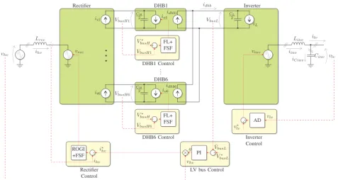
Figure 2 shows a general diagram of the chosen topology. The SST is composed of a bidirectional multi-level HV three-phase converter, labeled Recti-fier, six bidirectional isolated DC-DC converters, la-beled DHB1 through DHB6, and a bidirectional LV three-phase converter with neutral, labeled Inverter. This topology has a great degree of modularity, allow-ing to consider the converters as decoupled systems and simplifying the design of the controllers [7].
Each converter and its simplified model is de-scribed below. Since the controllers are implemented using digital control techniques, the models are de-scribed in discrete time, assuming a sampling timeTs.
2.1
Rectifier
The rectifier is a three-phase AC-DC converter con-nected to the HV grid. As shown in Figure 2, the recti-fier input port is modeled as a three-phase controlled voltage sourcevrec= [vrecavrecbvrecc]T, coupled to the HV grid voltagevhv= [vhvavhvbvhvc]T through an in-ductor with currentihv = [ihva ihvb ihvc]T. This cou-pling filter is modeled using complex vector notation (see Appendix). The zero order hold (zoh) discrete time model of the coupling filter results:
~ihv[k+ 1] =
Ts
Lrec
¯
~
vhv[k]−~vrec[k]
+~ihv[k], (1)
where ¯v~hv[k] = 0.5(v~hv[k+ 1] +~vhv[k]) is the mean value of the HV grid voltage in the time intervalTsk,
Ts(k+ 1).
The output ports of the rectifier are modeled as current sourcesiiX, withX= 1. . .6. These currents are computed through power balance. Considering that both H bridges of each phase of the rectifier are given the same reference, it can be found that their currents
are equal:
ii1[k] =ii2[k] =
vreca[k]ihva[k]
VbusH1[k] +VbusH2[k],
(2)
ii3[k] =ii4[k] =
vrecb[k]ihvb[k]
VbusH3[k] +VbusH4[k]
, (3)
ii5[k] =ii6[k] =
vrecc[k]ihvc[k]
VbusH5[k] +VbusH6[k]
. (4)
Note that in this rectifier model, the independent vari-ables (control inputs) are the three-phase components ofvrec[k].
2.2
Dual Half Bridge (DHB)
Since there are six isolated DC buses in the recti-fier, there are six DC-DC converters which are imple-mented using the DHB topology, which are modeled as current sources. The coupling between the output ports of the rectifier and the input port of each DHB is performed through a capacitor. The voltage across each of these capacitors is modeled through the diff er-ence equation:
VbusHX[k+ 1]=
Ts
CH/2
iiX[k]
−ioX[k]
+VbusHX[k], (5)
withX= 1. . .6. The DHBs themselves are controlled
using a phase shift strategy. Therefore, each converter can be modeled through the algebraic equation for their average power transfer [11]:
PdhbX[k]=
VbusHX[k]mVbusL[k]δX[k]
π
− |δX[k]|
8π2L dfswdhb
, (6)
wheremis the DHB transformer relation,Ldis the to-tal leakage of the transformer referred to the HV side,
fswdhbis the switching frequency of the DHB converter, andδX is the phase shift angle between the voltages generated at the HV and LV sides of the DHB under consideration. Dividing this power by VbusHX[k], it results
ioX[k] =
mVbusL[k]δX[k]
π
− |δX[k]|
8π2L dfswdhb
, (7)
which describes the relation between input port ioX and the control actionδX. The outputs of all the DHBs are connected in parallel, and feed the LV bus. The relation between the input signals and the output sig-nals is obtained through power balance, as described in the following equation:
idhbX[k] =
ioX[k]VbusHX[k]
VbusL[k]
. (8)
Figure 2:SST topology, model and general control scheme.
2.3
Inverter
The inverter is a three-phase DC-AC converter con-nected to the LV grid. The input port is modeled as a controlled current source iL, and the output port is modeled as a three-phase controlled voltage source
vinv = [vinvr vinvs vinvt]T. The load voltage and cur-rent arevlv= [vlvr vlvs vlvt]T andilv = [ilvr ilvsilvt]T, respectively.
The coupling between the output ports of the DHBs and the input port of the inverter is performed through a capacitor. The voltage across this capacitor is modeled through the difference equation:
VbusL[k+ 1] =
Ts
CL/2
idhb[k]
−iL[k]
+VbusL[k], (9)
where
idhb[k] = 6
X
X=1
idhbX[k]. (10)
The coupling between the load and the output port of the inverter is performed by an LC filter. Since each leg of the inverter is controlled as a single phase con-verter, the zoh discretization of this filter is given for each phase of the inverter. This is denoted with sub-scriptY, which can be equal tor,sort:
xinvY[k+ 1]=AinvxinvY[k]+BinvvinvY[k]+Binv1ilvY[k], (11)
wherexinvY[k] = [iinvY[k]vlvY[k]]T,
Ainv=
cos(√ Ts
CinvLinv) −
q
Cinv
Linvsin(
Ts √
CinvLinv)
q
Linv
Cinvsin(
Ts
√
CinvLinv) cos(
Ts
√
CinvLinv)
, (12)
Binv=
q
Cinv
Linvsin(
Ts √
CinvLinv) 1−cos(√ Ts
CinvLinv)
, (13)
Binv1=
1−cos(√ Ts
CinvLinv) −
q
Linv
Cinvsin(
Ts √
CinvLinv)
. (14)
As in the previous converters, the relation between the input signals and the output signals is obtained through power balance, as described in the following equation:
iL[k] =
vinv[k]•ilv[k]
VbusL[k]
, (15)
where the • operator denotes scalar product. Note
that in this inverter model, the independent variables (control inputs) are the three-phase components of
vinv[k].
3
Converter controller description
Figure 2 shows the simplified block diagrams of the proposed controllers for each converter. In this figure, dashed lines represent measured signals, and solid lines in the controllers represent control signals. In what follows, each individual controller is described.
3.1
Rectifier control
This controller is tasked to make the HV grid cur-rent ihv to copy the current reference i
∗
achieved through a full state feedback (FSF) control with the addition of a reduced order generalized inte-grator (ROGI) [12]. The ROGI is added to achieve zero steady state tracking error, since the current reference is a grid frequency positive sequence three-phase sig-nal. Considering a one sample time processing de-lay, typical in digital implementations, complex vec-tor notation, and space vecvec-tor modulation (SVM), the control action is
vrec[k] =v
∗
recSV M[k−1], (16)
vrecSV M∗ [k] =vrec∗ [k]−vmc[k], (17)
vmc[k] = 0.5 (max(v
∗
rec[k]) + min(v
∗
rec[k])), (18) where max and min functions are computed between theabccomponents ofvrec∗ [k]. Also,
~
vrec∗ [k] =−Krec
~ihv[k]−~ihv∗[k]
~
vrec∗ [k−1]
~r1[k]
, (19)
~r1[k+ 1]=j(1−ejωTs)
~ihv[k]
−~i∗
hv[k]
+e
jωTs~r
1[k], (20)
withKreca 1×3 complex gain vector, and~r1[k] repre-sents the state of a ROGI tuned at fundamental grid angular frequencyω. As described in [12], gain vec-torKreccan be found using the linear quadratic regu-lator method, or by pole placement using Ackerman’s formula, and the matrix description of the system:
xrec[k+ 1] =Arecxrec[k] +Brec~v
∗
rec[k], (21)
wherexrec[k] = [~ihv[k]~vrec∗ [k−1]~r1[k]]T,
Arec=
1 − Ts
Lrec 0
0 0 0
j(1−ejωTs) 0 ejωTs
, (22)
Brec= [0 1 0]T. (23)
The referenceihv∗ is the output of the LV bus con-troller, and it is related to the instantaneous HV grid voltage through
ihv∗ [k] =g[k]vhv[k], (24)
wheregis a scalar variable signal. Therefore, depend-ing on the sign ofg and assumingvhvsinusoidal with no harmonic distortion, the rectifier will source or sink a three-phase sinusoidal current to the HV grid, with unity power factor. In this paper the closed loop poles are chosen to achieve a settling time of 4.5[ms].
3.2
DHB control
The objective of the DHBs is to transfer the pulsating power of each of the H bridges of the rectifier to the LV bus, where the resulting power is non-pulsating. To achieve this objective, the controller of each DHB is designed to keep its instantaneous voltageVbusHXat its reference levelVbusH∗ (which is the same for all six DHBs). As shown by (7), the relation between current
ioXand phase-shift angleδX is non-linear. In order to be able to apply linear control techniques, a feedback linearization (FL) is implemented. Then, the resulting linear system is controlled through FSF.
Considering a one sample time processing delay, the control action is
δX[k] =δ
∗
X[k−1], (25)
where
δ∗X[k]=0.5π
1− s
1−32fswdhb |i ∗
oX[k]|
mVbusL[k]
sign(i∗oX[k]),
(26)
is obtained from (7) and it is the FL equation for the system. Assuming that VbusL[k] ' VbusL[k−1] (slow varying signal), it can be numerically verified that for a given value ofioX∗ [k−1], evaluating (26) at k−1, and replacing the result in (25) and (7) yields ioX[k]'ioX∗ [k−1]. Therefore, the linearized system is modeled by (5) and
ioX[k] =i
∗
oX[k−1]. (27)
Adding a discrete time backward Euler integrator to achieve zero steady state error, the control action for each DHB is computed as follows:
ioX∗ [k] =−KDHB
VbusHX[k]−V
∗
busH[k]
r0[k]
ioX[k]
, (28)
r0[k+ 1] =Ts
VbusHX[k]
−V∗
busH[k]
+r0[k], (29)
whereKdhb is a 1×3 gain vector, andr0[k] represents the state of the discrete integrator. Once (28) is com-puted, the phase shift angleδ∗X is obtained through (26) and applied to the converter.
Gain vector Kdhb can be found using the linear quadratic regulator method, or by pole placement us-ing Ackerman’s formula, and the matrix description of the linearized system:
xdhb[k+ 1] =Adhbxdhb[k] +Bdhbi
∗
oX[k], (30)
wherexdhb[k] = [VbusHX[k]r0[k]ioX[k]]T,
Adhb=
1 0 − Ts
CH/2
Ts 1 0
0 0 0
, (31)
Bdhb= [0 0 1]T. (32)
3.3
LV bus control
This controller is tasked to keep the mean value of the LV bus voltage ( ¯VbusLin Figure 2) at the reference level
VbusL∗ . In order to do so, signalVbusL is filtered (filter not shown in the figure) and then a proportional in-tegral (PI) controller is used. The output of this con-troller is the variable gaing. This gain is used to prop-erly scale the measured HV grid voltage, and generate the current reference for the rectifier, defined in (24). For this reason, the dynamics of the rectifier control loop and the LV bus control loop must be decoupled. This is achieved by making the bus control loop sig-nificantly slower than the rectifier and DHB control loops.
The LV bus voltage is modeled by (9). Since there is no controlled current source directly connected to the LV bus, the design of the controller assumes that
idhbis the control action. Once the control actionidhb is computed, gain g is obtained through power bal-ance:
g[k] =idhb[k] ¯VbusL[k]
3Vnomhv2 , (33)
whereVnomhvis the nominal rms value of the HV grid voltage. As stated at the beginning of this section, this controller is slow. Therefore, both the processing de-lay and the dynamics of the filter used to obtain ¯VbusL can be ignored without significant error. Considering this, and adding a discrete time backward Euler inte-grator to achieve zero steady state error, the control action is computed as follows:
idhb[k] =−KLV
"¯
VbusL[k]−V
∗
busL[k]
r0LV[k]
#
, (34)
r0LV[k+ 1] =T s
¯
VbusL[k]−V
∗
busL[k]
+r0LV[k], (35)
where KLV is a 1×2 gain vector, and r0LV[k] repre-sents the state of the discrete integrator. Once (34) is computed, gaingis computed through (33), and used to generate the HV grid current referenceihv∗ through (24).
Gain vector KLV can be found using the linear quadratic regulator method, or by pole placement us-ing Ackerman’s formula, and the matrix description of the system:
xLV[k+ 1] =ALVxLV[k] +BLVidhb[k], (36)
wherexLV[k] = [VbusL[k]r0LV[k]]T,
ALV =
"
1 0
Ts 1
#
, (37)
BLV = [ Ts
CL/2
0]T. (38)
In this paper the closed loop poles are chosen to achieve a settling time of 100[ms].
3.4
Inverter control
This controller implements the active damping (AD) of the output LC filter resonance. The implemen-tation of the AD requires to measure the current throughCinv. To avoid this measurement, an estima-tor through high pass filter derivation is used. This estimator only requires the measurement ofvlv, and only slightly increases the settling time of the control loop. The LV grid voltage reference vlv∗ is added to the control action of the AD. This voltage reference is a three-phase balanced sinusoidal signal, which can be generated internally, or can be obtained through a synchronization algorithm in synchronism with the HV grid voltage.
Since each leg of the inverter is controlled inde-pendently, there are three equal controllers. In what follows, they are described with subscriptY =r,sor
t. Considering a one sample processing time, the con-trol action for the active damping strategy isvinvY[k] =
vinvY∗ [k−1], where
vinvY∗ [k] =−Klv
ˆ
iCinvY[k]
vlvY[k]
vinvY∗ [k−1]
+K∗vlvY∗ , (39)
where Klv is a 1×3 gain vector, K∗ is a gain, and ˆ
iCinvY[k] is the estimated capacitor current, obtained from the zoh discretization of a high pass filter:
ηY[k+ 1] = (e
−ωcTs
−1)vlvY[k] +e−ωcTsη
Y[k], (40)
ˆ
iCinvY[k] =Cinvωc
vlvY[k] +ηY[k]
, (41)
withωc the cut off frequency of the high pass filter, andηY the state of the filter.
Gain vector Klv is obtained by pole placement to damp the LC filter resonance using Ackerman’s for-mula, and the matrix description of the system:
xlv[k+ 1] =Alvxlv[k] +Blvv
∗
invY[k], (42) wherexlv[k] = [iinvY[k]v
∗
invY[k−1]vinvY[k]]T,
Alv=
"
Ainv Binv
0 0 0
#
, (43)
Blv= [0 0 1]T. (44)
Finally, gainK∗is included to compensate the magni-tude of the LV grid voltage reference, and is obtained evaluating:
T F=Clv(z I−ACLlv )
−1 Blv
z=ejωTs, (45)
K∗=|1/T F|, (46)
whereACLlv =Alv−BlvKlv, I is the 3×3 identity matrix andClv = [0 1 0]. Note that the controllers for each phase use the same gain vector Klv and gainK
∗
4
Parameter selection criteria
This section gives criteria for choosing the values of the different parameters of each converter.
4.1
Rectifier coupling inductance
L
recFigure 3:Rectifier phaseaand switching interval variables.
The value ofLrecis chosen to obtain a desired current ripple4iwhen injecting zero current to the HV grid.
Due to the 5-level structure of the rectifier and the use of unipolar modulation, the effective switching fre-quency applied to Lrec is 4fswrec [1]. Also, this multi-level structure ensures that the voltage difference ap-plied toLrecwill never be larger thanVbusH∗ (assuming all the HV buses are kept at that level).
Taking phaseaas a reference, Figure 3 shows one switching interval. The current variation in this inter-val is
4i= Ton
Lrec
(vhva−V
∗
busH). (47)
Since zero current injection is assumed, in this inter-val
vhva'V
∗
busHd, (48)
whered=Ton/T. Therefore, replacing this in (47),
4i= V ∗
busH
Lrec4fswrec(d
2−d), (49)
whereT = 1/(4fswrec) was used. The maximum4i oc-curs ford= 0.5, therefore for this condition, from (49),
Lrec=
VbusH∗
4i16fswrec. (50)
From Table 1, choosing the peak current ripple4i/2 =
0.1(
√
2Inomhv), the inductance resultsLrec= 190[mH]. From an additional analysis not included in this pa-per, considering commercially available cores,Lrec= 200[mH] is chosen.
4.2
DHB transformer leakage inductance
L
dFrom (6), assumingVbusHX[k] =V
∗
busH andVbusL[k] =
VbusL∗ =VbusH∗ /mthe maximum power transfer occurs forδX[k] =π/2 and results
PdhbMAX=
(VbusH∗ )2 32Ldfswdhb
. (51)
Under nominal operation conditions, each DHB will have to transfer a mean power ¯Pdhb=Snom/6. Taking a safety margin ofPdhbMAX= 2 ¯Pdhbto catch any tran-sients, and replacing this in (51), the leakage induc-tance results
Ld=
3(VbusH∗ )2 32Snomfswdhb
. (52)
Using the necessary parameters from Table 1 to eval-uate (52), it results Ld = 8.44[mH]. From an addi-tional analysis not included in this paper, designing
Ldconsidering commercially available cores, it results
Ld= 8.8[mH] .
4.3
HV bus capacitor
C
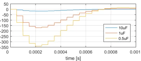
HFigure 4:4VbusH[V] for a 10% HV grid voltage dip for different values ofCH.
During the event of dips or swells in the HV grid voltagevhv, there will be a transient behavior in each of the HV buses. This can lead to unacceptable un-der/over voltages in VbusHX. The HV buses voltage variations during these transients are determined by the value ofCH, the settling time of each DHB con-trol loop, and the magnitude of the dips or swells. Since the evaluation of these transients involves the DHB control loop, the process is iterative. For a given value ofCH, gainKdhb must be computed. Then, the performance is evaluated through a simple simulation applying the desired dip or swell magnitude. Finally, the process is repeated until the desired performance is attained.
The evaluation is performed considering a step change in the magnitude ofvhv. In the following, the worst case scenario forVbusH1 is analyzed, which is similar for the remaining buses.
The maximum instantaneous power variation in phasea occurs when the rectifier is sinking nominal current, and at the instantaneous peak of vhva[k] its magnitude changes 4vhv volts. From (1), assuming
that previous to the stepv~hv'~vrec, the magnitude of the change in the HV grid current is
4ihv' Ts Lrec
4vhv. (53)
From (2), assuming that previous to the stepVbusH1=
VbusH1=VbusH∗ , the variation in currentii1is
4ii= √
2Vnomhv4ihv 2VbusH∗ =
Ts
Lrec
√
2Vnomhv4vhv
where (53) was used for the last equality. Now the ef-fect of4vhvinVbusH1, defined as4VbusH, is evaluated
simulating the closed loop response of the linearized DHB (30)-(32):
4xdhb[k+ 1] =Acl
dhb4xdhb[k] +Bidhbi 4ii, (55)
4VbusH[k] = [1 0 0]4xdhb[k], (56)
whereBii
dhb = [ Ts
CH/2 0 0]
T andAcl
dhb=Adhb−BdhbKdhb. Figure 4 shows simulation results for this system for
CH = 10 [µF], 1[µF] and 0.5[µF] when a 10% dip is simulated (4vhv = −0.1Vnomhv) for the DHB control
designed with a settling time of 1[ms]. From the re-sultsCH = 1 [µF] is chosen, since it results in a 2.5% voltage variation.
4.4
LV bus capacitor
C
LFigure 5: 4VbusL[V] for a nominal load sudden connection and
different values ofCL.
The value of capacitorCLis chosen so that in the event of a sudden nominal load connection, the LV bus volt-age does not go below the minimum value required for normal operation. The minimum LV bus voltage required for operation is
VbusLMIN= 2
√
2Vnomlv= 622V , (57)
where the value is obtained from Table 1. Therefore, a conservative design criterion is to keepVbusL>700V when a nominal load is connected. This is equivalent to obtain a LV bus voltage variation4VbusL<100V.
To evaluate the LV bus voltage variation for dif-ferent values ofCL, gain vectorKLV is computed for each given value, and then a simulation is performed. From (36)-(38), the following system is simulated:
4xLV[k+ 1] =Acl
LV4xLV[k] +BclLV4iL, (58)
4VbusL[k] = [1 0]4xLV[k], (59)
whereACLLV =ALV −BLVKLV, BclLV =−BLV and 4iL =
Snom/V
∗
busL. Figure 5 shows simulation results for this system for CL = 5 [mF], 10[mF] and 15[mF] when a nominal load is suddenly connected and the LV bus voltage control loop is designed with a settling time of 100[ms]. From the results all capacitor values meet the requirements, howeverCL= 10 [mF] is chosen be-cause of reduced ripple under unbalanced load condi-tions.
4.5
Inverter filter
L
invC
invThe typical output impedance of a standard trans-former is 2%-5% of its base impedance. Therefore,
Linv is chosen so that its impedance at angular fre-quencyωis 2% of the base impedance:
Linv= 0.02
3Vnomlv2
ωSnom
= 462 [µH]. (60)
On the other hand, capacitor Cinv limits the band-width of the output. Here, to obtain a fast transient response, the cut-offangular frequency of the output filter is chosen
ωcut−of f = 20ω. (61)
Since the resonance frequency of the filter is approxi-mately equal to the cut-offfrequency,
ωres'ωcut−of f =
1
√
LinvCinv
, (62)
then
Cinv=
1 (20ω)2L
inv
= 55 [µF]. (63)
5
Operation analysis of the
con-trol system and simulation
re-sults
This section presents simulation results of the pro-posed SST when a load is suddenly connected and disconnected. Additionally, results for sudden non-linear load connection are included. The results are obtained using the switching models of all converters. The system parameter summary is shown in Table 1.
Table 1: System parameter summary
RECTIFIER AND LV BUS
Param. Value Description
Snom 20[kVA] SST nominal power
Vnomhv 7621[Vrms] HV nom. phase voltage
Inomhv 0.875[Arms] HV nom. phase current
f 50[Hz] HV grid frequency
Lrec 200[mH] HV filter inductance
VbusL∗ 800[V] LV bus reference
CL 10[mF] LV bus capacitor
frec
sw 8[kHz] Switching frequency
DHB
CH 1[µF] HV bus capacitor
CLdhb 56[µF] LV DHB capacitor
Ld 8.8[mH] DHB leakage ind.
VbusH∗ 6000[V] HV bus reference
m 7.5 Transformer relation
fswdhb 20[kHz] Switching frequency INVERTER
Linv 461.2[µH] LC filter ind.
Cinv 55[µF] LC filter cap.
Vnomlv 220[Vrms] LV phase voltage
The controllers were designed so that the rectifier trol loop has a settling time of 4.5[ms], the DHB con-trol loop has a settling time of 1[ms], and the LV bus voltage control loop has a settling time of 100[ms]. The settling time of the inverter AD loop is defined by the cutofffrequency of its LC output filter plus the estimation of the current throughCinv. This settling time results approximately 2[ms].
5.1
Sudden load connection
Figure 6:vlv[V] sudden load connection.
Figure 7:ilv[A] sudden load connection.
Figure 8:VbusL[V] sudden load connection.
Figure 9:vhv[V] sudden load connection.
Figure 10:ihv[A] sudden load connection.
Figure 11:VbusH1−VbusH6[V] sudden load connection.
The simulation results shown in Figures 6-11 start at
t= 0.18[s] with the SST in steady state, with no load connected on the LV side. This means that the HV and LV buses start at their reference voltage levels and that a balanced three-phase sinusoidal voltagevlvis gener-ated without taking significant current ihv from the HV grid.
Att= 0.2[s] a resistive nominal load is connected at the inverter output. The following sequence of events occurs (refer to Figure 2 for the definition of the variables):
• Figures 6 and 7 show vlv andilv, respectively. As expected, when the load is connectedvlvhas a short transient.
• Through power balance, current sourceiLtakes current from capacitor CL, reducing voltage
VbusLas shown in Figure 8. As can be seen, its settling time is approximately 100[ms], as de-signed.
• The LV bus voltage control loop detects the re-duction of ¯VbusL, increasing in turn the value of
g, resulting ing >0. As a result, current refer-enceihv∗ magnitude increases.
• Commanded by its current controller, the recti-fier sinks active power from the grid, with unity power factor. Figures 9 and 10 showvhvandihv, respectively. Here the settling time of the cur-rent is tied to the settling time ofg, defined by the LV bus control loop.
• Through power balance, the current source out-puts of the rectifier charges capacitorsCHof the HV buses, increasing their voltage levels. The voltages of the HV buses is shown in Figure 11.
• The control loop of each DHB detects the increase in their respective HV bus voltage
VbusHX. As a result, it commands each DHB to sink currentioX in order to decrease the in-stantaneous valueVbusHX to its reference value
VbusH∗ once again. This results in the short transient increase in the mean value of voltages
VbusHX seen in Figure 11. Through power bal-ance, each output currentidhbX sources current to the LV bus, charging CL to V
∗
busL again, as shown in Figure 8.
5.2
Sudden load disconnection
Figure 12:vlv[V] sudden load disconnection.
Figure 13:ilv[A] sudden load disconnection.
Figure 14:VbusL[V] sudden load disconnection.
Figure 15:vhv[V] sudden load disconnection.
Figure 16:ihv[A] sudden load disconnection.
Figure 17:VbusH1−VbusH6[V] sudden load disconnection.
Starting from the previous condition, if the load is now disconnected, the following sequence of events will occur:
• Figures 12 and 13 showvlvandilv, respectively. As expected, when the load is disconnectedvlv has a short transient.
• Through power balance, current source iL stops sinking current from capacitorCL, which charges because the DHBs are still transferring power from the HV grid. This is seen in Figure 14.
• LV bus voltage control loop detects the voltage increase in ¯VbusL, decreasing in turn the value of
g, resulting ing <0. As a result, current refer-enceihv∗ magnitude decreases.
• Commanded by its current controller, the recti-fier goes from sinking to supplying active power to the grid, with unity power factor. Figures 15 and 16 showvhvandihv, respectively.
• Through power balance, the current source out-puts of the rectifier discharge capacitors CH of the HV buses, decreasing their voltage levels, as seen in Figure 17.
• The control loop of each DHB detects the decrease in their respective HV bus voltage
VbusHX. As a result, it commands each DHB to source current ioX in order to increase the in-stantaneous valueVbusHX to its reference value
VbusH∗ once again. This results in the short tran-sient decrease in the mean value of voltages
VbusHX seen in Figure 17. Through power bal-ance, each output current idhbX sinks current from the LV bus, dischargingCL toVbusL∗ again, as shown in Figure 14.
By the end of this sequence, in steady state, the system has its buses at their reference values, and the inverter generatesvlvwithout sinking currentihvfrom the HV grid.
5.3
Sudden non-linear load connection
Figure 18:vlv[V] sudden non-linear load connection.
Figure 19:ilv[A] sudden non-linear load connection.
Figure 20:VbusL[V] sudden non-linear load connection.
Figure 21:vhv[V] sudden non-linear load connection.
Figure 22:ihv[A] sudden non-linear load connection.
Figure 23: VbusH1−VbusH6[V] sudden non-linear load
connec-tion.
5.4
Sudden non-linear unbalanced load
connection
The simulation of the previous section is repeated, us-ing the same non-linear load, but connectus-ing these loads to only two of the three phases. The results of this simulation are shown in 24-29. As can be seen in these results, the proposed topology also works well for unbalanced non-linear loads.
Figure 24: vlv[V] sudden non-linear unbalanced load connec-tion.
Figure 25: ilv [A] sudden non-linear unbalanced load connec-tion.
Figure 26:VbusL[V] sudden non-linear unbalanced load connec-tion.
Figure 27: vhv[V] sudden non-linear unbalanced load connec-tion.
Figure 29: VbusH1−VbusH6[V] sudden non-linear unbalanced
load connection.
6
Conclusions
In this paper a model and a control strategy for an SST topology is proposed. The analyzed SST is de-signed using three separate stages: a rectifier, a DC-DC converter and an inverter. The proposed design approach is to model each stage using simple models. These simple models help to design and tune the con-trollers for each stage. The main focus of the tuning procedure is to obtain good performance to sudden load connections. Criteria to choose the main param-eters of the SST are also given.
To validate the proposed method, simulation re-sults are presented. The rere-sults show that the pro-posed topology and control strategies perform as ex-pected from design conditions. Moreover, the staged design of the SST allows to decouple the HV side from the LV side in regard to load disturbances, which is an additional feature of the SST when compared to tradi-tional transformers. Simulations were performed for both linear and linear loads. Moreover, a non-linear unbalanced load was also tested, with good per-formance results.
Acknowledgment The authors are grateful to CON-ICET, UNIVERSIDAD NACIONAL DEL SUR and AN-PCyT for their institutional and economic support
Appendix
Given a three-phase signalf = [fafbfc]T, itsαβ com-ponents are obtained through Clarke’s transform:
"
fα
fβ
#
=2 3
"
1 −0.5 −0.5
0
√
3/2 −p(3)/2
#
fa
fb
fc
. (64)
Then, the complex vectorf~is defined as
~
f =fα+jfβ, (65)
wherej=
√ −1.
References
[1] C. Busada, H. Chiacchiarini, S. G. Jorge, F. Mengatto, A. Oliva, J. Solsona, G. Bloch, and A. Delgadillo, “Mod-eling and control of a medium voltage three-phase solid-state transformer,” in 2017 11th IEEE International Con-ference on Compatibility, Power Electronics and Power Engi-neering (CPE-POWERENG), April 2017, pp. 556–561. DOI: 10.1109/CPE.2017.7915232
[2] J. Van der Merwe and H. d. T. Mouton, “The solid-state transformer concept: A new era in power distri-bution,” in AFRICON 2009, 2009. DOI: 10.1109/AFR-CON.2009.5308264
[3] G. T. Heydt, “The next generation of power distribution sys-tems,”IEEE Transactions on Smart Grid, vol. 1, no. 3, pp. 225– 235, 2010. DOI: 10.1109/TSG.2010.2080328
[4] S. Falcones, X. Mao, and R. Ayyanar, “Topology com-parison for solid state transformer implementation,” in
IEEE PES General Meeting. IEEE, 2010, pp. 1–8. DOI: 10.1109/PES.2010.5590086
[5] X. She, R. Burgos, G. Wang, F. Wang, and A. Q. Huang, “Re-view of solid state transformer in the distribution system: From components to field application,” in2012 IEEE Energy Conversion Congress and Exposition (ECCE). IEEE, 2012, pp. 4077–4084. DOI: 10.1109/ECCE.2012.6342269
[6] X. She, A. Q. Huang, and R. Burgos, “Review of solid-state transformer technologies and their application in power dis-tribution systems,”IEEE Journal of Emerging and Selected Top-ics in Power ElectronTop-ics, vol. 1, no. 3, pp. 186–198, 2013. DOI: 10.1109/JESTPE.2013.2277917
[7] J. W. Kolar and G. Ortiz, “Solid-state-transformers: key com-ponents of future traction and smart grid systems,” inProc. of the International Power Electronics Conference (IPEC), Hi-roshima, Japan, 2014.
[8] F. Wang, A. Huang, X. Niet al., “A 3.6 kv high performance solid state transformer based on 13kv sic mosfet,” in2014 IEEE 5th International Symposium on Power Electronics for Dis-tributed Generation Systems (PEDG). IEEE, 2014, pp. 1–8. DOI: 10.1109/PEDG.2014.6878693
[9] J. E. Huber and J. W. Kolar, “Volume/weight/cost compari-son of a 1mva 10 kv/400 v solid-state against a conventional low-frequency distribution transformer,” in2014 IEEE En-ergy Conversion Congress and Exposition (ECCE). IEEE, 2014, pp. 4545–4552. DOI: 10.1109/ECCE.2014.6954023
[10] Z. Yu, R. Ayyanar, and I. Husain, “A detailed analytical model of a solid state transformer,” in2015 IEEE Energy Conversion Congress and Exposition (ECCE). IEEE, 2015, pp. 723–729. DOI: 10.1109/ECCE.2015.7309761
[11] H. Fan and H. Li, “High-frequency transformer isolated bidi-rectional dc-dc converter modules with high efficiency over wide load range for 20 kva solid-state transformer,” IEEE Transactions on Power Electronics, vol. 26, no. 12, pp. 3599– 3608, Dec 2011. DOI: 10.1109/TPEL.2011.2160652
![Figure 2 shows a general diagram of the chosentopology.The SST is composed of a bidirectionalmulti-level HV three-phase converter, labeled Recti-fier, six bidirectional isolated DC-DC converters, la-beled DHB1 through DHB6, and a bidirectional LVthree-phase converter with neutral, labeled Inverter.This topology has a great degree of modularity, allow-ing to consider the converters as decoupled systemsand simplifying the design of the controllers [7].](https://thumb-us.123doks.com/thumbv2/123dok_us/10073567.1993789/2.595.342.538.79.159/chosentopology-bidirectionalmulti-bidirectional-bidirectional-modularity-systemsand-simplifying-controllers.webp)
![Figure 5: △VbusL [V] for a nominal load sudden connection anddifferent values of CL.](https://thumb-us.123doks.com/thumbv2/123dok_us/10073567.1993789/7.595.307.535.509.784/figure-vbusl-nominal-load-sudden-connection-anddierent-values.webp)
![Figure 11: VbusH1 − VbusH6 [V] sudden load connection.](https://thumb-us.123doks.com/thumbv2/123dok_us/10073567.1993789/8.595.314.527.61.148/figure-vbush-vbush-v-sudden-load-connection.webp)
![Figure 12: vlv [V] sudden load disconnection.](https://thumb-us.123doks.com/thumbv2/123dok_us/10073567.1993789/9.595.66.290.76.768/figure-vlv-v-sudden-load-disconnection.webp)
![Figure 29: VbusH1 − VbusH6 [V] sudden non-linear unbalancedload connection.](https://thumb-us.123doks.com/thumbv2/123dok_us/10073567.1993789/11.595.69.283.63.147/figure-vbush-vbush-sudden-non-linear-unbalancedload-connection.webp)
