Iranian Journal of Electrical and Electronic Engineering, Vol. 15, No. 4, December 2019 485
Efficient Delay Characterization Method to Obtain the Output
Waveform of Logic Gates Considering Glitches
S. Abolmaali*(C.A.)
Abstract: Accurate delay calculation of circuit gates is very important in timing analysis of digital circuits. Waveform shapes on the input ports of logic gates should be considered, in the characterization phase of delay calculation, to obtain accurate gate delay values. Glitches and their temporal effect on circuit gate delays should be taken into account for this purpose. However, the explosive number of combinations of waveform shapes, which can be applied to the input ports of logic gates, causes existing lookup-based methods to have huge space requirements. In this article, instead of considering all possible combinations of waveform shapes in the characterization phase of delay calculation process, the least number of combinations, which are dominant in determining the waveform shape of gate output, is presented. Multivariate Polynomial Regression (MPR) method is used to further reduce the required memory space. Exploration of the possible MPR analyses is performed to find the best regression case with proper memory space reduction and precision. Attained results show a 1.013E6 times reduction in storage space required for storing parameters utilized in extraction of output waveform characteristics in comparison to a state of the artwork, accompanied by acceptable precision.
Keywords: Delay Calculation, Delay Characterization, Signal Waveform, Glitch, Multivariate Polynomial Regression.
1 Introduction1
BTAINING the maximum delay of a digital circuit is vital to reliably utilize the circuit under maximum speed, without violating circuit timing constraints. Timing analysis methods are used to find the critical paths of circuit. In static timing analysis methods (instead of dynamic method which is based on repetitive circuit simulations) delays of circuit gates are summed to attain delays of circuit paths. Therefore, obtaining precise values for delays of circuit gates leads to more accurate values for delays of circuit critical paths.
To obtain gate delays, delay calculation methods are utilized. These methods have two phases. In the first phase, which is called delay characterization phase, the
Iranian Journal of Electrical and Electronic Engineering, 2019. Paper first received 02 March 2019, revised 20 April 2019, and accepted 27 April 2019.
* The author is with the Electrical and Computer Engineering Department, Semnan University, Semnan, Iran.
E-mail: [email protected]. Corresponding Author: S. Abolmaali.
gate delay is attained considering several circuit parameters like the load capacitance of gate, the slope delays and waveform shapes of input signals, and etc. This phase can be performed in a general manner for each logic gate type and independent to the containing circuit. In the second phase, the delay computation phase, the delay of each circuit gate is computed considering the gate input signals constructed by applying two separate test vectors to the primary inputs of circuit. One or more quantities obtained in the first phase are combined together properly to achieve the final gate delay.
To attain accurate gate delay values by a delay calculation method, considering the waveform shapes of input signals is very important. Waveform shapes should be considered in the characterization phase to provide a powerful library for the delay computation phase. Especially, creation of glitches and the responses of different gate types to the created glitches on their input lines should be included in this process. There are two general methods for characterization: model-based and lookup-based. In the model-based method, the logic gate is modeled by an equivalent simpler circuit, with
O
Iranian Journal of Electrical and Electronic Engineering, Vol. 15, No. 4, December 2019 486 one or more linear or non-linear circuit components
(like resistors, capacitors, dependent current source, and etc.). The models are developed as a way that the responses of the logic gate and its corresponding model be the same for special input signals.
In the lookup-based method, several lookup tables are generated. The responses of each gate type to a set of pre-defined waveform shapes on the gate input signals, for a number of considered circuit parameters, like the load capacitance and the slope delay of input signal, are stored in these tables. Interpolation and extrapolation methods are utilized in the computation phase by using proper entities of the tables to compute the gate delay for a set of circuit parameter values.
Many previous works are about accurate analysis of glitches when they are passing through a logic gate [1-10]. Introducing proper gate models for propagation, degradation and filtering of input glitches are studied in these researches. In many of these works, they only concentrate on the glitch peak voltage and not on the glitch width, which is important in accurate timing analysis. Moreover, their concentration is only on the behavior of a gate in eliminating or propagating an input glitch. The effect of probable transitions and waveforms on the other input ports of the gate is not considered in their analyses.
There are plenty of the previous works which developed useful gate models utilized in delay calculation [11-20]. Many of them introduce gate delay models only for complete input transitions, and glitches and more complex waveforms are not considered in their works. In addition, early researches in this area consider transition on single input port of gate. Those works which consider multiple input switching do not involve glitches in the input transitions. Moreover, in many of these works, the input switchings happen simultaneously and input transitions with different transition times are not considered. Additionally, most of them do not examine their proposed delay models in delay calculation of logic gates of a circuit with many logic gates. In this case, two input vectors should be applied to the primary inputs of the circuit separately, which produce different waveform shapes on the circuit lines. This truth shows that many of them do not concentrate on the analyses of the gate responses to the complex waveforms which can appear on one or more input ports of circuit gates. Simple circuits like ring oscillators are used in many of them to validate their delay models.
A most recent work, based on waveform lookup, has been introduced in [21]. In this approach, switching events on different gate inputs that occur in close temporal proximity are grouped into event combinations. The output voltage response of each combination is then looked up from the library and the potentially overlapping voltage responses are combined to shape properly the output waveform. The obtained waveform is analyzed to retrieve the relevant signal
characteristics which are stored in the local database for use in subsequent estimations. This solution benefits well from runtime advantage of lookup-based methods with the accuracy of analog signal waveforms. However, the huge number of event combinations results in considerable space complexity, especially when more accurate waveform shapes are considered. In this article a waveform-lookup-based approach is presented for delay characterization. Instead of considering many number of close temporal proximities and huge number of event combinations, only a restricted set of waveform combinations, constructed by the least number of complete transitions and static glitches, and are dominant in shaping the output waveforms is presented. The main idea is that every complex waveform shape can be decomposed to a number of complete transitions and glitches. In addition, only waveform combinations on two gate inputs are taken into account, instead of multiple input waveform combinations, to reduce the total number of combinations.
The number of required storage also decreases by applying regression on the values of parameters which denote the shape of output waveforms. Instead of storing input waveform combinations and their related characterizing output waveform parameters, only coefficients obtained from applying regressions on them are stored. As it will be shown in Section 4, the dependence of output waveform characteristics to the considered circuit parameters can be depicted by several different curves. In general, these curves have different shapes which can be fitted by different mathematical functions. Here, the diversity of curve shapes is high. On the other hand, according to the Taylor’s theorem, every differentiable function can be estimated by a series of Taylor polynomials. Thus, polynomial regression is utilized in this work, which can estimate many non-linear functions efficiently and has the best estimation errors.
In addition, using multivariate regression methods results in more reduction of memory space required for storing the quantities, in comparison to the single-variable methods. Therefore, Multivariate Polynomial Regression (MPR) is used in this research. To find the best degree of regression polynomial for each case, regression calculation is performed for degrees 1 to 4 in all cases. Larger degree values results in small precision improvement in the cost of storing more regression coefficients. It should be mentioned that decrease in the number of stored quantities leads to reduction in program load time in applications using these quantities. As stated previously, the proposed method of this article is related to the characterization phase. In the computation phase, it is necessary to construct the waveform shape of a gate output based on the complex waveform shapes on its input ports. To achieve this, the values obtained in the first phase should be combined in a sophisticated manner. This will be the goal of the
Iranian Journal of Electrical and Electronic Engineering, Vol. 15, No. 4, December 2019 487 future works.
One last point which should be mentioned is that in this work, the environmental and process variations are not considered. The focus of this work is on obtaining the precise waveform shapes of circuit lines, which requires considering deterministic and accurate values for circuit parameters. Including variations necessitates using random variables, with statistical distributions, for circuit parameters which are not proper for the process of finding precise waveform shapes. Before considering variations, a comprehensive and accurate delay calculation method should be developed for the case where circuit parameters have deterministic values. Generalizing the obtained method to the statistical one in the presence of variations will be the topic of the future works.
The rest of the article is organized as follows. In Section 2, input waveform shapes and combinations which participate in constructing most of waveform shapes on output ports of gates, are presented. In Section 3, characteristic lookup tables required for constructing the output waveform shapes are presented, including the tables required for introduced combinations. In addition, circuit parameters which the values of table entities are dependent to them are presented. Section 4 explains the algorithms used for performing MPR analysis on each extracted lookup table. Section 5 contains the results and discussion. Finally, conclusion of the article and future work are given in Section 6.
2 Dominant Input Waveform Combinations
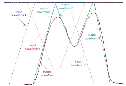
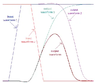
In this section, input waveform shapes and combinations which participate in constructing most of the waveform shapes on output ports of gates, are presented. These waveforms are attained from this observation that every complex waveform can be decomposed to a number of complete transitions and static glitches. Fig. 1 shows a set of illustrating waveform shapes. One rising transition, one glitch and one falling transition are considered for input ports of a 3-inputs AND gate. The output waveform contains of two peaks and a valley between them. One approximation choice for the output waveform is proposed in the figure including three output waveforms 1, 2 and 3. From this example, it can be concluded that complex waveform shapes can be approximated by combining a number of simpler waveform shapes. As stated previously, the construction of these approximated output waveform based on the mentioned input waveforms is related to the computation phase and is relegated to the future works.
By understanding this observation, the considered waveform combinations are presented. Following two factors contribute in choosing the introduced waveform combinations: (1) the input signal transitions are in the same direction or opposite direction; (2) glitches exist in
Fig. 1 Estimation of complex waveforms with two or more complete transitions and glitches.
the input signals or not. On the other hand, in this work, only waveform shapes on two input ports of gates are considered, to reduce the number of combinations which should be stored for waveform lookup. It is believed that by accepting a tolerable error penalty, proper waveform shape on the output of a gate can be constructed by considering waveforms on two input ports first and then applying the effect of waveform shapes of other input ports on constructing the waveform shape of output port of the gate. Moreover, it is considered in this work that only one transition or glitch can appear in input waveform shapes. More complicated input waveforms can be decomposed into a number of mentioned simple waveforms. As stated, the two latter cases are the subjects of the future researches.
2.1 Definitions
First, a number of definitions used frequently in this article are presented.
Complete transition: A transition which has a complete swing from zero voltage to supply voltage, or from supply voltage to zero voltage. It can be a dynamic glitch, which have one change in the voltage swing direction.
Incomplete transition: A transition with incomplete swing between zero voltage and supply voltage. A static glitch consists of two incomplete transitions. Static glitches are those which the value of signal is the same before and after glitch occurrence.
Slope delay: The time from start of a (complete or incomplete) transition till the finish of transition swing.
Online input: An input port of a gate which receives a considered transition.
Side input: An input port of a gate other than the online input.
Critical timing window: For a transition on online input of a gate, the minimum time interval which starts before the transition and finishes after the transition, and expected that in this time interval the side input of gate to have stable non-controlling value to allow the transition on the online input passes completely (without creating incomplete transition on the gate
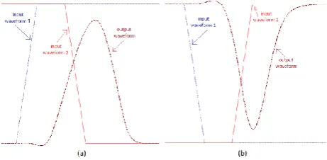
Iranian Journal of Electrical and Electronic Engineering, Vol. 15, No. 4, December 2019 488 Fig. 2 Waveforms to show the effect of approximating the
input signals by linear pieces.
output) through the gate.
2.2 Linear Approximation for Waveform Shapes
The transitions in the waveforms are not completely linear and have a number of curves. Saving the exact information of a waveform shape is difficult and needs storing several coefficients related to the formula for proper fitting curve. Instead, the waveform shape is approximated by a piecewise-linear function. More the number of linear pieces means less approximation error. In Fig. 1, the input waveforms and three output waveforms 1, 2 and 3 are represented by linear waveform shapes.
It should be mentioned that in this work, the input signals used for delay characterization are also approximated by linear pieces. By looking at the waveforms in Fig. 2, it is obvious that this approximation imposes very little error. Input waveforms 1 and 2 are the real and the approximated input signals, respectively. Output waveforms 1 and 2 are the responses of a 2-inputs AND gate to these input signals, respectively, which are very close to each other. It can be seen that the curve at the end of the transition of input waveform 1 has a negligible effect on the characteristics of the output waveform.
On the other hand, as is depicted in Fig. 1, in this work the output waveform of a gate is decomposed into a number of linear pieces. The waveform on the output of a gate acts as the input waveform for the fan-out gates. Therefore in the proposed method, circuit gates receive input signals approximated by piecewise-linear waveforms. This is the reason that linear waveforms are used for input signals in the delay characterization process.
2.3 Considered Combinations
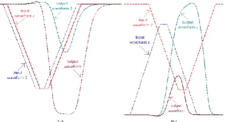
Combination 1 (Comb_1): The two input signals have transitions in opposite direction and are close to each other. Two possible cases for this combination is depicted in Fig. 3, along the example waveforms on the gate output. This combination is the source of glitch
Fig. 3 Waveforms for explaining combination Comb_1.
Fig. 4 Waveforms for explaining combination Comb_2.
creation on circuit lines. No glitch is formed if the two transitions do not place in close proximity. The two input signals may be on single input port or may place on two separate input ports.
Fig. 3(a) shows the case when two input signals have overlap in logic value 1. Related output waveform is for the gate types which have non-controlling value 1, like AND and NAND gates. For gate types with non-controlling value 0, like OR and NOR gates, the output signal is constant 1 (since always at least one of input ports has logical value 1). Fig. 3(b) is related to the case where two input signals have overlap in logic value 0. The relevant output waveform is for the gate types which have non-controlling value 0.
Combination 2 (Comb_2): The two input signals have transitions in the same direction and are close to each other. Two possible cases for this combination is depicted in Fig. 4, along the response waveforms on the gate output. Since the transitions are in close proximity, they are inside of critical timing window of each other and the input signals do not act for each other like the side inputs having perfect non-controlling value. Therefore, the output transition (output waveform 1) has different delay in comparison to the case that the side input has perfect constant non-controlling value (output waveform 2). The output waveforms are obtained for a 2-inputs AND gate and the delay difference between two output waveforms can be several picoseconds. In Fig. 4(a), input waveform 1 constructs the output waveform 2 since the second input considered having stable non-controlling value. On the other hand, input waveform 2 is dominant in determining the output waveform 1 since it transit to non-controlling value later than the first transition. This is the reason why output waveform 1 is after output waveform 2. In Fig. 4(b),
Iranian Journal of Electrical and Electronic Engineering, Vol. 15, No. 4, December 2019 489 Fig. 5 Waveforms for explaining combination Comb_3.
Fig. 6 Waveforms for explaining combination Comb_4.
output waveform 2 is also constructed by input waveform 1 since the second input considered having stable non-controlling value. However, for output waveform 1, since the second input port transit to the controlling value together with the first input port, resistance of the gate against transition of its output to controlling value is less than the case where the second input pin has a non-controlling value. Thus, output waveform 1 has earlier transition to logical value 0.
Combination 3 (Comb_3): One of input ports has a single static glitch in its waveform and the other input port has a stable non-controlling value. Fig. 5 shows the existence of glitch in input waveforms and the responses of an AND gate to these glitches. Note that this combination is also applicable to single input gates i.e. buffers and inverters. In case (a), input and output waveforms contain a static-1 glitch, and in case (b) a static-0 glitch is appeared in each waveform.
Combination 4 (Comb_4): One of input ports has a single static glitch in its waveform and the other input port has a complete transition. Fig. 6 depicts two illustrating cases for an AND gate. The output waveforms are complete transitions which are dynamic glitches. Although not showed in the figure, it is obvious that the output waveforms have different shapes and delays in comparison to the case where the second input port has a stable non-controlling value.
Combination 5 (Comb_5): Both of input ports have a single static glitch in their waveforms. Fig. 7 shows two examples for a 2-inputs AND gate. In Fig. 7(a), two static-0 glitches are applied to the gate’s input ports. In Fig. 7(b), one static-1 glitch and one static-0 glitch on input ports feed the gate.
Waveform named output waveform is the response of the gate to two input glitches in each case. Output
Fig. 7 Waveforms for explaining combination Comb_5.
waveform 2 is the response of a similar gate which has the input waveform 1 on its first input port and a stable non-controlling value on the other input port. It is obvious that the presence of a glitch on the side input of a gate, instead of a stable non-controlling value, can change the output waveform significantly.
3 Extraction of Required Lookup Tables
In this section, characteristic lookup tables required for constructing the output waveform shapes are presented, including the tables required for introduced combinations. A sample algorithm used for extraction of one of these tables is also presented. In addition, circuit parameters which the values of table entities are dependent to them are introduced.
3.1 Important Considered Circuit Parameters
In this subsection, some circuit parameters that should be considered in the extraction process of a delay value or a waveform shape of gate response are presented. For each considered parameter, a range of varying values should be applied in the extraction process to obtain the amount of dependence of the output response to that parameter.
Gate type (gt_typ): For a given input transition, the propagation and slope delays of different gate types are not the same. This is related to the internal circuit of each gate type which is made from transistors. In this work, BUFFER, INVERTER, AND, OR, NAND and NOR gate types are considered. For gate types having more than one input port, gates with 2, 3 and 4 input ports are included (total 14 gate types).
Input port number (fanin_num): For a given input transition and a given gate type, the propagation and slope delays of different input ports are not the same. This is due to the location of the transistor, which receives the input signal, in the gate internal circuit.
Transition type (trans_typ): For a given gate type and a given input port, the propagation and slope delays of gate for input rise and fall transitions are not the same. This is due to different transistor types and different sub-circuits which are responsible for driving the output port to high or low voltage levels.
Iranian Journal of Electrical and Electronic Engineering, Vol. 15, No. 4, December 2019 490 Load capacitance (ld_cap): When a logic gate places
in a circuit, the gates that are derived by this gate induce a load capacitance on the output port of the gate. Other circuit components like circuit wires also can add load capacitances. These capacitances change the slope delay and propagation delay of output transitions. Indeed, increase in the value of such capacitances makes growth of the time constant of equivalent RC circuit at the output port of a gate. In this article, only load capacitances imposed by fan-out gates are considered.
Input slope delay (in_slp_dly): The other important parameter is the slope delay of input transition. If the input slope delay becomes larger, the output slope delay also becomes greater.
Time Distance between input transitions
(in_transs_dist): It is the time distance between the start
times of two transitions in two separate input ports. This parameter is dominant in cases like Comb_1. Less distance in this case means less probability of creating glitches on output ports.
Type of input glitch (in_glch_typ): The response of the gate to a static-1 glitch and a static-0 glitch, with the same glitch characteristics, is not the same.
Peak value of input glitch (in_pk_val): For static-1 and static-0 glitches, the peak value represents the maximum value and the minimum value of related waveforms, respectively. The peak value is determinant in the ability of glitch in passing through the gate, or in the output waveform deformation when the glitch places on a side input.
Glitch width (in_glch_w): It is the time between the glitch start and the glitch vanishing, for static glitches. It is related to the slope delays of two constructing transitions of glitch. Larger glitch width means more capability of glitch in passing through the gate.
In extraction of each entity of a table, SPICE simulation is used to obtain accurate values. Running multiple SPICE simulations is a very time-consuming process. However, this is performed only once and after preparation of a table, its content can be utilized several times. SPICE sub-circuits described in NanGate45 Open Cell library [22] for each gate type are used in this work. According to the selected library, the timing values measured by SPICE simulations are not less than 1 picosecond. Thus, time unit equal to 1 picosecond is considered in this work.
3.2 Extraction of Load Capacitances of Gates Placing in a Circuit
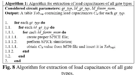
The algorithm for extraction of load capacitances of all gate types is presented in Fig. 8 as a sample extraction algorithm. The extraction process is performed for each gt_typ. This is because different gt_typ’s have different equivalent capacitances on their output ports when the same load gate type is placed on their output ports. For example, a 4-inputs NOR as load of a BUFFER and as load of a 4-inputs NOR induces
Fig. 8 Algorithm for extraction of load capacitances of all gate types.
0.669 femtofarads and 0.733 femtofarads equivalent capacitances, respectively.
On the other hand, each gate type as the load (ld_gt_typ) of a given gt_typ has a specific equivalent capacitance. Therefore, for a given gt_typ, the extraction process is performed for each ld_gt_typ. Furthermore, the load capacitance is also dependent to the input port number of the load gate (ld_fanin_num). Thus, for a given gt_typ and a given ld_gt_typ, the extraction process is performed for each ld_fanin_num.
The extraction process for obtaining each entry of the table is as follows. First, a SPICE file is created. In this file, a pulse signal is included with 15 picoseconds for rise and fall transitions. The pulse signal is used as the input signal of each gt_typ. Two instances of gt_typ are inserted in the file. One has an ld_gt_typ as its load and the other has the parameter CLOAD as load. The CLOAD value is varying from 0.4 femtofarads to 9.0 femtofarads with 0.01 femtofarads steps. To consider all of these values in one simulation run, SWEEP capability of SPICE is used. Proper measure commands are inserted in the file to attain the low-to-high and high-to-low propagation delays (tplh and tphl) of each
gt_typ instance. Then, the SPICE simulation is performed on the prepared file. By reading the measured delays included in the MT0 file, the CLOAD which makes the average value of tplh and tphl equal for two gt_typ instances is the equivalent load capacitance. The obtained value is inserted in Tabcap table. To access each entry of Tabcap, it is indexed by gt_typ, ld_gt_typ and ld_fanin_num.
3.3 Extraction of Typical Delays of Each Gate Type
The considered circuit parameters for this case are: gt_typ, fanin_num, ld_cap, in_slp_dly, and trans_typ. Four delay values tplh, tphl, tr (rise time) and tf (fall time) are attained in each iteration of this algorithm. Different ld_cap values are considered on the output of gate types to investigate the dependence of delay values to ld_cap values. To attain more precise results, a wide range of ld_cap values are considered. According to the equivalent capacitive loads extracted by Algorithm 1, ld_cap values from 0.4 femtofarads to 9.8 femtofarads are used in this work with 0.2 femtofarads step value. In addition, in this case, values from 12 picoseconds to 190
Iranian Journal of Electrical and Electronic Engineering, Vol. 15, No. 4, December 2019 491 picoseconds with step value equal to 2 picoseconds are
considered for in_slp_dly.
Obtaining above four delay values is performed for each gt_typ, each fanin_num of gt_typ, each ld_cap value and each in_slp_dly value in the above-mentioned ranges. The extracted entities are stored in Tabtyp_dly table. It should be mentioned that obtained tr and tf can be used as the slope delays of rise and fall transitions on the output port, respectively.
3.4 Extraction of Output Waveforms Parameters Related to Comb_1
Fig. 9 shows the case where two input transitions are close to each other and thus, the output transitions on the output waveform become incomplete, preparing the conditions for creating a glitch.
In this work, all the cases, from the case in which the output transition has a small peak value to the case that the output transitions pass completely, are considered. One may suggests that by using the entities of table Tabtyp_dly presented in Subsection 3.3, the propagation delays and slope delays of output transitions can be obtained and by having them, the peak value of the glitch is computable. However, by taking a look at the figure, it is inferred that this approach is not applicable. In the figure, output waveform 1 is the response of the gate to the input waveform 1, when the other input port have stable non-controlling value. The output waveform 2 is obtained similarly. As is obvious, the two mentioned output waveforms do not place exactly on the main output waveform of gate. Specially, the peak values are not the same, and the second transition of created glitch happens earlier in comparison to the output waveform 2. Therefore, it is necessary to obtain the peak value (pk_val) and the difference in propagation delays of second transitions (out_dly_chng) by accurate SPICE simulations.
The characteristics of created glitch are dependent to the slope delays of input transitions. To reduce the number of participating parameters, in this work it is assumed that one slope delay value is used for both input transitions. To obtain the slope delays of output transitions, output waveforms in Fig. 9 is analyzed. By looking at the first transition of output waveform and output waveform 1, it is apparent that the slopes of these transitions are almost the same. Similar situation happens for the second transition of output waveform and output waveform 2. Therefore, by measuring the pk_val and having the slope delays of output waveforms 1 and 2 (obtained by the procedure explained in Subsection 3.3), slope delays of output transitions are attained. These assumptions impose little error percentage.
Considered circuit parameters in this case are: gt_typ, fanin_num, ld_cap, in_slp_dly, and in_transs_dist. First, it should be noted that more precise values are obtained when for each gt_typ, all input port pairs are considered.
Fig. 9 Waveforms for explaining the response of a 2-input AND gate to two close input transitions in opposite directions.
This causes multiple-times growth in the number of table entities. This case is mitigated by assuming that in all input port pairs, one is always the first input port. Second, it may be expected that trans_type to be one of the considered circuit parameters. The reason for exclusion of trans_type is described as follows. If we consider a falling transition occurs earlier than a rising transition, instead of input waveforms of Fig. 9, in each time point at least one of the input ports has controlling value 0. Therefore, the gate output always has logical 0 and no transition happens on the output port. Thus, for AND NAND gate types, only one transition type can be considered for each of two input waveforms. Similar situation is valid for OR and NOR gate types.
In this case, in_transs_dist values are in the range from 0 to 424 picoseconds with step value 1 picosecond. Since the pk_val and out_dly_chng values are very sensitive to in_transs_dist parameter in some cases, 1 picosecond step value is used here. Moreover, to attain the pk_val of output glitch, MIN (for static-0 glitch) and MAX (for static-1 glitch) modes of SPICE measure command are utilized. The extracted pk_val and out_dly_chng values are inserted in table TabComb_1.
3.5 Extraction of Output Waveforms Parameters Related to Comb_2
Considered circuit parameters in this case are: gt_typ, fanin_num, trans_type, ld_cap, in_slp_dly, and in_transs_dist. Each entry of the resulted table (TabComb_2) is a ratio quantity (dly_chng_ratio). It is obtained by dividing the gate delay for output waveform 1 in Fig. 4 to the gate delay for output waveform 2. It can be deducted from the figure that the ratio value can be less than or greater than 1. The attained ratio value is then inserted in TabComb_2 table.
3.6 Extraction of Output Waveforms Parameters Related to Comb_3
In this case, the considered circuit parameters are: gt_typ, fanin_num, in_glch_typ, ld_cap, in_glch_w, and in_pk_val. The algorithm obtains pk_val and glch_w
Iranian Journal of Electrical and Electronic Engineering, Vol. 15, No. 4, December 2019 492 values of the static glitch on the output port. The impact
of ld_cap on the output waveform parameters should be considered for a wide range in this case. Related values are varying from 0.5 femtofarads to 10.1 femtofarads with 0.04 femtofarads steps.
In this case, each input glitch is specified by its width (in_glch_w) and its peak value (in_pk_val). Values from 30 picoseconds to 222 picoseconds with step value equal to 8 picoseconds are used for in_glch_w to cover a wide range. As little change in peak value of input glitch may cause considerable shift in the pk_val of output glitch when the ld_cap is not large, the range from 0.1 volts to near supply voltage value (1.09 volts in this work) with step value 0.01 volts is specified for in_pk_val in this case. Obtained values for pk_val and glch_w of the glitch on the gate output are inserted in TabComb_3 table.
3.7 Extraction of Output Waveforms Parameters Related to Comb_4 and Comb_5
For Comb_4, gt_type, fanin_num, trans_type and in_slp_dly of input complete transition, in_glch_typ, in_glch_w and in_pk_val of input glitch on the other input port, in_transs_dist between above two input waveforms, and ld_cap should be considered in the extraction process. For Comb_5, among the above circuit parameters, instead of trans_type and in_slp_dly of input complete transition, in_glch_typ, in_glch_w and in_pk_val of input glitch on online input of gate should be considered. Since the number of parameters which should be taken into account is many for the above mentioned combinations and the extraction procedure is complicated, the related algorithms are not included in this work and are postponed to the next work.
4 Performing MPR on the Entries of Obtained Tables
According to the number of circuit parameters considered in extraction of entities of above tables, and keeping in mind that for each circuit parameter a range (wide range in many cases) of values are considered, the number of entities of tables grows substantially. As a result, a large memory space is required to store the tables. To overcome this obstacle, regression analysis on the entries of each obtained table is utilized to reduce the required memory space. This way, regression coefficients instead of table entries are stored.
There are several regression techniques to estimate the relationship between the obtained values. Since each attained table is indexed by more than one circuit parameter, multivariate regression methods should be employed. On the other hand, the relationship between the table entities, based on considered circuit parameters, is not the same for different considered circuit parameters. For one parameter, the relationship might be linear, and for another one the relationship might be from higher degrees. This behavior can be
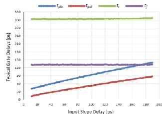
Fig. 10 Dependence of typical gate delays to in_slp_dly.
observed in Fig. 10 through Fig. 17. Since for each table, the number of related sets of values is very high, it is not possible to analyze the sets one-by-one to find the best approximating formula for each set. The situation becomes worse when more than one circuit parameter is considered for estimation. Thus, a general regression analysis method is required to be profitable in many approximation cases.
By using the Taylor’s theorem for multivariate functions [23], the required regression technique can be selected. According to this theorem, having function f :RnR
, which is a k times differentiable
function at the point n
R
a , there exists h : n R R such that:
!
k k
D f
f h
a
x x a x x a
and
lim h 0
x a x
in which, x is the vector of variables and Dαf(a) is the α-th derivative of f(x) in point a. In other words, any multivariate function can be approximated by a series of polynomial terms. Therefore, MPR technique is a good choice in this work to be utilized in many approximation cases. By considering several polynomial degrees, a comprehensive approximation analysis is performed. The maximum value considered for the polynomial degree should not be very big since, although the accuracy of the approximation becomes better, however it causes the number of regression coefficients grows substantially.
In this work, for each extracted table, several combinations of circuit parameters are considered as the variables of regression analysis. For each given combination, all polynomial regressions with degrees from 1 to 4 are examined. The goal of performing this great number of regression analyses is to find the best case which results in considerable reduction of required memory space with acceptable error penalty.
In this section, regression analyses on the previously extracted tables are presented. A sample algorithm is introduced to clarify the complexity of the proposed
Iranian Journal of Electrical and Electronic Engineering, Vol. 15, No. 4, December 2019 493 Fig. 11 Dependence of typical gate delays to ld_cap.
method. The circuit parameters which are considered as regression variables are ld_cap, in_slp_dly, in_transs_dist and in_pk_val. These parameters are those which a range of monotonic values are assigned to them in extraction of lookup tables presented in Section 3. In the following algorithm REGRES_VARS_SET is the set of circuit parameters which are considered as regression variables. Since table Tabcap is not indexed by the above considered parameters, it is excluded from this analysis. The results of performing regression analyses are presented in the next section.
4.1 Regression Analysis on Tabtyp_dly
Figs. 10 and 11 show the dependence of typical gate delays to the changes of circuit parameters. Values depicted in Fig. 10 are for the typical delays related to the fourth input port of a 4-inputs NOR gate, and are for changes of in_slp_dly. Results in Fig. 11 are for the fourth input port of a 4-inputs AND gate, and are for changes of ld_cap. As is obvious, all charts are approximately linear.
Due to the lack of paper space, the related regression algorithm is not shown here. The algorithm prepares for each typical delay kind dly_kind a number of tables Tabtyp_dly_regres__dly_kind__poly_deg__regres_vars_comb. Each table is related to a considered polynomial degree poly_deg and a regression variables combination regres_vars_comb. Each table contains the regression coefficients for all gate types and all input port numbers of gate types. For each dly_kind, each gt_typ and each fanin_num, several files are prepared based on regres_vars_comb to be used in the regression analysis. Two nested loops are implemented to fill the context of regression files by values of regression variables and delay values from the entities of table Tabtyp_dly. The table is indexed by
gt_typ, fanin_num, ld_cap, in_slp_dly and dly_kind to access a delay value dly.
If regres_vars_comb contains both variables ld_cap and in_slp_dly, one regression file is filled by the nested loops. All value combinations of regression variables ld_cap and in_slp_dly are written in the separate rows of file by nested loops. In addition, in each row, the delay value dly indexed by ld_cap and in_slp_dly of that row also is written in the file. After filling the file, a
Fig. 12 Output pk_val values for a number of in_transs_dist
values when all output pk_val values are considered.
Fig. 13 Output pk_val values for a number of in_transs_dist
values when only varying pk_val values are considered.
MPR with degree poly_deg is performed on the file and the obtained regression coefficients are stored in table Tabtyp_dly_regres__dly_kind__poly_deg__ld_cap__in_slp_dly. The number of regression coefficients is dependent to the value of poly_deg. However, since for all value combinations of regression variables only one regression analysis is performed, the reduction in memory storage is considerable. This is the case when more than one regression variables are considered in MPR. Nonetheless, in these cases, the error penalty increases. If regres_vars_comb contains only the variable ld_cap, the parameter of first nested loop is in_slp_dly and for the second one is ld_cap. For each in_slp_dly in its considered range, a regression file is created based on regression variable ld_cap and a regression analysis is performed on the file. Therefore, several regression analyses are performed in this case. In the rows of regression file, in addition to ld_cap values, the delay values dly obtained from table Tabtyp_dly, which is indexed by only one in_slp_dly but several ld_cap values, are also written. Similar processes are performed when regres_vars_comb contains only the variable in_slp_dly.
4.2 Regression Analysis on TabComb_1
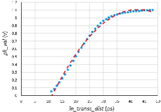
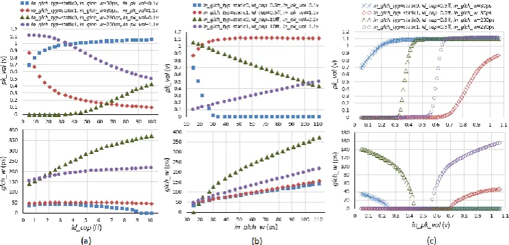
Fig. 12 shows pk_val values for a number of in_transs_dist values. For in_transs_dist values greater than 45 picoseconds, pk_val is stable at 1.1 volts. For charts like this, approximation with polynomial regression (the dashed line in figure) even with a high degree value (4 for this case) results in non-ignorable
Iranian Journal of Electrical and Electronic Engineering, Vol. 15, No. 4, December 2019 494 Fig. 14 Normalized pk_val and out_dly_chng values relative to
in_transs_dist values.
Fig. 15 Normalized pk_val and out_dly_chng values relative to
ld_cap values.
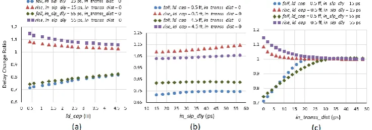
Fig. 16 Delay change ratios stored in TabComb_2 for different values of a) ld_cap, b) in_slp_dly, and c) in_transs_dist.
error (about 0.1 volts for this case). It is because of the parts that pk_val is stable. To overcome this problem, only the chart part that pk_val is varying is considered (Fig. 13). It is apparent from the figure that the dashed line (with degree 2) is very close to the main chart. The in_transs_dist values for the start and end of the main chart in Fig. 12 should be stored (here, 11 and 49). Fig. 14 and Fig. 15 depict normalized pk_val and out_dly_chng values for different in_transs_dist and ld_cap values, respectively. Parameter in_slp_dly is not considered here since the dependence of pk_val and out_dly_chng values to in_slp_dly is negligible. In Fig. 15, the stored start and end values explained in the previous paragraph are used for in_transs_dist. While the dependence to ld_cap is approximately linear, it is from higher degrees for in_transs_dist.
The algorithm performing regression analyses prepares for pk_val and out_dly_chng a number of tables, based on different values for poly_deg and regres_vars_comb. Each table contains the regression coefficients for all gate types and all input port numbers of gate types. REGRES_VARS_SET is constructed by ld_cap, in_slp_dly and in_transs_dist. Three single-element, three two-elements and one three-elements subsets are obtained for this set. For a regression file, regres_vars_comb is a subset of REGRES_VARS_SET. Several text files are prepared in the algorithm based on regres_vars_comb to be used in the regression analysis. Three nested loops are implemented to fill the context
of regression files by values of regression variables, and values of pk_val or out_dly_chng. To access values of pk_val or out_dly_chng, table TabComb_1 is indexed by
gt_typ, fanin_num, ld_cap, in_slp_dly and in_transs_dist.
If regres_vars_comb contains all three regression variables, one file is filled by the nested loops. All value combinations of regression variables are written in the separate rows of file by nested loops. In addition, in each row, values of pk_val and out_dly_chng obtained by indexing TabComb_1 also are written in the file. After filling the file, a MPR with degree poly_deg is performed on it and the obtained regression coefficients are stored in a lookup table.
If regres_vars_comb contains two variables, several regression files are filled by two inner nested loops. The number of files is equal to the number of values considered for the third regression variable. Each file is filled similar to the case when regres_vars_comb contains three variables. After that, several MPR with degree poly_deg are performed on the files and the obtained regression coefficients are stored in a lookup table. The number of stored coefficients increases since several MPRs are performed. If regres_vars_comb contains only one variable, only the inner loop fills the context of the regression files. Many (multiplication of sizes of two outer loops) text files are created and a MPR is performed for each one. The obtained regression coefficients are stored in a separate table.
Iranian Journal of Electrical and Electronic Engineering, Vol. 15, No. 4, December 2019 495 Fig. 17 Values of pk_val and glch_w for different values of a) ld_cap, b) in_glch_w, and c) in_pk_val.
Table 1 Number of coefficients of polynomial functions for different number of regression variables and different
polynomial degree.
Nregres_vars Polynomial Degree
1 2 3 4
1 2 3 4 5
2 3 6 10 15
3 4 10 20 35
4.3 Regression Analysis on TabComb_2
Fig. 16 shows delay change ratios, related to the case where two input signals have transitions in the same direction, for different values of ld_cap, in_slp_dly and in_transs_dist. While the dependences in first two charts are close to linear, it is from higher degrees for the last one. The algorithm for performing regression analysis for this case is very similar to that in the previous subsection since here REGRES_VARS_SET also includes ld_cap, in_slp_dly and in_transs_dist.
4.4 Regression Analysis on TabComb_3
Charts (a), (b) and (c) in Fig. 17 depict values of pk_val and glch_w for different values of regression variables ld_cap, in_glch_w and in_pk_val, respectively. It can be observed that in most cases the relation of pk_val and glch_w to regression variables is non-linear. The flow of algorithm for performing regression analysis is similar to that in Subsection 4.2, except that regression variables differ in these algorithms.
5 Results and Discussions
In this work, SPICE sub-circuits described in NanGate45 Open Cell library [22] for each gate type are used. The considered supply voltage and temperature are 1.1 volts and 25 degree Celsius, respectively. As stated in Section 3, which is about the extraction of required lookup tables, a number of circuit parameters are considered in the extraction process of each table
entry. These parameters are included in the SPICE model used in the extraction of table entries. A range of values for each circuit parameter is considered and therefore, several SPICE files are simulated to obtain the entries of each lookup table. In each mentioned subsection, the considered circuit parameters are listed. For example, for extracting typical delays of each gate type in Subsection 3.3, for each value of gt_typ, fanin_num, ld_cap, in_slp_dly, and trans_typ, a separate SPICE file is created and is simulated to attain a table entry.
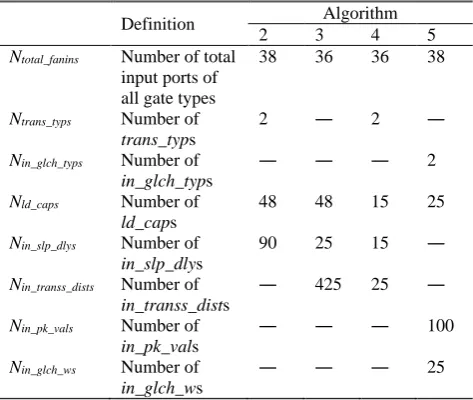
Table 1 shows the number of coefficients of polynomial function obtained by performing regression analysis for different values of the number of regression variables (Nregres_vars) and different values for polynomial degree. It is used in the rest of this section to obtain the number of quantities that are stored for each regression analysis.
A number of important parameters in extracting entity values of tables introduced in Section 3 were presented in Subsection 3.1. The number of entities of each table is dependent to the number of circuit parameters considered in the extraction process of the table, and the range of values considered for each parameter. Among these parameters, those considered as regression variables are listed in Section 4. The rest of parameters determine that the extraction process is performed for which type of transition or for glitch on which input port of what gate type. The number of all cases that different values of these parameters create is named NPARAM_CASES in the rest. When it is desired to calculate the reduction ratio in required space when regression analysis is used, NPARAM_CASES has no effect since the number of regression analyses performed for each subset of regression variables is a coefficient of this parameter. The reduction ratio is dependent to the subset of regression variables used in each regression analyses. In addition, Ntotal_extract_vals refers to the number of total values stored in each extracted table presented in Section 3. Moreover, Ntotal_regres_coefs is defined as the
Iranian Journal of Electrical and Electronic Engineering, Vol. 15, No. 4, December 2019 496 Table 2 Some definitions used in the subsequent subsections
and their possible values for each algorithm.
Definition Algorithm
2 3 4 5
Ntotal_fanins Number of total input ports of all gate types
38 36 36 38
Ntrans_typs Number of
trans_typs
2 ― 2 ―
Nin_glch_typs Number of
in_glch_typs
― ― ― 2
Nld_caps Number of
ld_caps
48 48 15 25
Nin_slp_dlys Number of
in_slp_dlys
90 25 15 ―
Nin_transs_dists Number of
in_transs_dists
― 425 25 ―
Nin_pk_vals Number of
in_pk_vals
― ― ― 100
Nin_glch_ws Number of
in_glch_ws
― ― ― 25
total number of regression coefficients resulted from performing a regression analysis with a given regres_vars_comb and a given poly_deg, NPARAM_CASES times. Furthermore, some definitions which are used in the subsequent subsections and their possible values for each algorithm are introduced in Table 2. Algorithms 2 through 5 are those used in the extraction of lookup tables in Subsections 3.3 through 3.6, respectively. To explain the values considered for Ntotal_fanins, as stated previously, totally 14 gate types (BUFFER, INVERTER, in addition to AND, NAND, OR, NOR gates with 2, 3 and 4 input ports) are considered in this work. For algorithms in which all gate types are used (like Algorithms 2 and 5), in aggregate, 38 input ports participate in the procedure. For algorithm in which gate types with more than one input ports are considered (like Algorithms 3 and 4), the quantity is 36 (excluding input ports of BUFFER and INVERTER). Furthermore, Ntrans_typs is equal to 2 for rise and fall transition types. Moreover, static-1 and static-0 glitch types make Nin_glch_typs equal to 2.
In addition to the number of entities in each extracted table, the number of regression coefficients resulted by different regression analyses is also reported in this section. These mentioned values are used in calculating the memory space reduction ratios attained by regression analyses. Furthermore, the error penalties implied by using the results of regression analyses are also presented. Because of huge number of error values, maximum and average error values are reported. For a regression variable subset and a polynomial degree, all the extracted values for all values of circuit parameters which are considered as regression variables are compared with the values obtained by using regression results. Then, maximum and average values of attained error value set are determined. This procedure is performed for each gt_typ, each fanin_num and each trans_typ or each in_glch_typ, which results in
several maximum and average error values. Using these error values, minimum of maximum error values (max_errmin), maximum of maximum error values (max_errmax) and its percentage to the actual extracted value (max_errmax(%)), average of maximum error values (max_erravg), minimum of average error values (avg_errmin), maximum of average error values (avg_errmax) and its percentage to the actual extracted value (avg_errmax(%)), and average of average error values (avg_erravg) are reported. Many information can be extracted from these reported error parameters.
5.1Results for Extraction of Load Capacitances
The number of values extracted in this case is dependent to the circuit parameters gt_typ, ld_gt_typ and ld_fanin_num. According to the above explanation about the gate types, gt_typ can have 14 quantities and combination of ld_gt_typ and ld_fanin_num can be one of the 38 cases. Therefore, total number of extracted quantities is 14×38=532 which should be stored in Tabcap. As stated before, no regression analysis is performed for this case.
5.2 Results for Extraction of Tabtyp_dly and Related
Regression Analyses
From circuit parameters presented in Subsection 3.3 and entities of Table 2, we have NPARAM_CASES = N-total_fanins × Ntrans_typs = 38×2 = 76. Accordingly, for each delay type, total number of extracted values is obtained by expression Ntotal_extract_vals = NPARAM_CASES × Nld_caps ×
Nin_slp_dlys = 76×48×90 = 328,320. Tables 3 and 4 show the results of performing several regression analyses for delay type tplh. The values of error parameters introduced previously are included in Table 3. Table 4 contains the number of regression coefficients for different regression variable subsets and different polynomial degrees, and also the reduction ratios in required memory space. The ratios are obtained by dividing the total number of extracted values (Ntotal_extract_vals) to the total number of regression coefficients (Ntotal_regres_coefs). In construction of Table 4, the contexts of Tables 1 and 2 are utilized. The expressions in column Ntotal_regres_coefs show how each entity value is obtained. For example, for the first row, the value is attained by multiplying NPARAM_CASES (76), and the number of regression coefficients for the regression case (2), and Nin_slp_dlys (90).
If we note to the last four columns of Table 3, it can be seen that all regression analyses are useful since the obtained average errors are no more than about 1.32 picoseconds. It is observed from column max_errmin that there are regression analyses that result in very small error since their maximum error values are very little. More, it is inferred from column max_errmax that for
poly_deg=1 the errors are the greatest. Anyhow, column max_erravg also admits that all regression analyses are
Iranian Journal of Electrical and Electronic Engineering, Vol. 15, No. 4, December 2019 497 Table 3 Error parameters for different polynomial degrees and different regression variable subsets, on entities of Tabtyp_dly.
Table 4 Number of regression coefficients and reduction ratios in required memory space, for different polynomial degrees and different regression variable subsets, on entities of
Tabtyp_dly.
poly_deg regres_vars_comb Ntotal_regres_coefs Reduction
Ratio (×) 1 {ld_cap} 76×2×90=13,680 24 1 {in_slp_dly} 76×48×2=7,296 45 1 {ld_cap, in_slp_dly} 76×3=228 1,440 2 {ld_cap} 76×3×90=20,520 16 2 {in_slp_dly} 76×48×3=10,944 30 2 {ld_cap, in_slp_dly} 76×6=456 720 3 {ld_cap} 76×4×90=27,360 12 3 {in_slp_dly} 76×48×4=14,592 22.5 3 {ld_cap, in_slp_dly} 76×10=760 432 4 {ld_cap} 76×5×90=34,200 9.6 4 {in_slp_dly} 76×48×5=18,240 18 4 {ld_cap, in_slp_dly} 76×15=1,140 288
useful since the obtained maximum errors are no more than 5.7 picoseconds in average. It is seen from the table that regres_vars_comb = {ld_cap, in_slp_dly} has the greatest error among all regres_vars_combs.
It is concluded from above inferences that using one regression variable with poly_deg=4 leads to the best precision. With more careful look to the entities of Table 3 it is deduced that using ld_cap instead of in_slp_dly results in smaller errors. Thus, regression variable ld_cap with poly_deg=4 has the least error. However, the reduction in the required memory space is another important factor to select a regression analysis case. It is observed from Table 4 that regres_vars_comb = {ld_cap, in_slp_dly} has the best reduction ratios since more extracted values participate in only one regression analysis. In addition, choosing poly_deg=1 results in more reduction ratios since polynomial functions with lesser degree have lesser number of coefficients. Therefore, regres_vars_comb = {ld_cap, in_slp_dly} together with poly_deg=1 has the best reduction ratio (1,440×). This is completely against the regression case that obtains the smallest errors.
Selecting the best regression case here is a tradeoff between precision and memory space. Tables 3 and 4 can be used to guide the decisions. An acceptable choice maybe the case regres_vars_comb = {ld_cap, in_slp_dly} with poly_deg=2, which has a considerable reduction ratio (720×) with reasonable max_errmax,
max_erravg and avg_erravg values equal to 3.33 picoseconds, 1.55 picoseconds and 0.3 picoseconds, respectively.
5.3 Results for All Lookup Table Extractions and Selected Regression Cases
Due to the lack of article pages, the detailed results of performing regression analyses on the remained algorithms of Section 3 are omitted. Instead, all the final results of all algorithms are gathered in one place, in Table 5. In this table, in column for regression case, BR means the best reduction ratio, BP means the best precision and MR means the most reasonable. For the sake of brevity, only one output value for each algorithm is considered. For Algorithm 2 delay value tplh, for Algorithm 3 delay value out_dly_chng, for Algorithm 4 ratio value dly_chng_ratio, and for Algorithm 5 value pk_val participate in Table 5.
Table 6 summarizes for Algorithms 2 through 5 the entity numbers of lookup tables (column 2), the number of coefficients obtained for regression analyses (column 3), the number of start and stop values required to be stored for Algorithms 3 and 5 (column 4), and the reduction ratio in the required memory space by performing regression analyses (column 5). Since Algorithms 2, 3 and 5 produce more than one output quantities, in columns 2 and 3 of the table, values Ntotal_extract_vals are multiplied to the number of outputs. In column 3, the number of extracted values is divided to the reduction ratios related to the regression analyses. These ratios are related to the most reasonable regression case.
The last column contains the reduction ratio for each table row. Each reduction ratio is obtained by dividing the value in column 2 to the sum of values in column 3 and 4 (if any). The last row shows the overall values for all algorithms. In its second column, the total number of entities in all lookup tables is depicted. The total number of values which should be stored by the suggested regression analyses is obtained by 958,660+181,400=1,140,060. Overall, a 42× reduction in the required memory space is obtained by this work. Note that since the number of extracted values for Algorithm 1 is small, it is ignored from above calculations.
Iranian Journal of Electrical and Electronic Engineering, Vol. 15, No. 4, December 2019 498 Table 5 Final results of all algorithms.
Table 6 Reduction ratios resulted by regression analyses for all algorithms.
5.4 Analysis of Sample Circuits to Examine the Precision of Approximations
In this subsection, the approximation methods used in this article are examined by analyzing some sample circuits. The investigations are performed for typical delays of gate types and the peak values on gate outputs for Comb_3. Constructing sample circuits for the results of Comb_1 and Comb_2 are useless. They should be checked in benchmark circuits containing several gates with complicated circuit structures which is out of the scope of this article.
5.4.1 Examining the Typical Delays of Gate Types
In this case, the sample circuit is constructed by placing instances from each gate type consecutively, making a circuit with 14 gates. The output of each instance gate is connected to an input port of the next instance gate. The input port is selected randomly. For each instance gate, in addition to the capacitive load induced by the load gate, a random load capacitance between 0.5 and 5 femtofarads is considered on the gate output port. Two rise and fall transitions with 15 picoseconds slope delay are applied to the input port of the first circuit gate in turn. The results of circuit simulation by SPICE and the results obtained by using our presented approximation method then are compared. This procedure is performed 1000 times.
For the rise transition on the input port of the first circuit gate, minimum error percentage, maximum error percentage and average error percentage become 0.26%, 9.17% and 4.65%, respectively which are acceptable. For the fall transition, values -1.08%, 8.96% and 3.71% are obtained respectively which are also satisfactory.
Many propagation and slope delays with different types are examined in this way for different values of load capacitances.
5.4.2 Examining the Peak Values on Gate Outputs
for Comb_3
To examine our approximation method in the case of the response of a gate instance to an input static glitch, the chain of gates with the same type is used. 14 circuits, each has a chain of 5 gates with the same type are constructed. For gate types with more than one input port, the first input port is considered. No additional load capacitances are included in this case. Both static-0 and static-1 glitches are considered as input waveform for each constructed circuit. The peak values and the widths of input glitches are chosen in a way that the glitches do not disappear very soon. Table 7 compares the peak values on the gate outputs obtained by our proposed method with those obtained by SPICE simulation.
For each gate type and each glitch type, three values are reported for the output port of each gate in the chain. The first and second values are the peak values obtained by this work and by the SPISE simulation, respectively. The third value is the percentage of error (difference between above mentioned values) relative to the value of supply voltage (1.1 volts). The last three columns of the table report minimum, maximum and average error percentages for each row. The last two rows show the maximum of above error percentages over all rows of the table. It can be observed from the last rows that the selected MR regression cases have good estimation precisions.
At last, it should be noted that the number of