Microstructure and Electrical Conductivity of CaRuO
3Thin Films Prepared by Laser Ablation
Akihiko Ito
1, Hiroshi Masumoto
2and Takashi Goto
21
Institute of Multidisciplinary Research for Advanced Materials, Tohoku University, Sendai 980-8577, Japan
2Institute for Materials Research, Tohoku University, Sendai 980-8577, Japan
CaRuO3(CRO) thin films were prepared by laser ablation at substrate temperatures (Tsub) ranging from room temperature to 1073 K in a high vacuum (106Pa) atmosphere and at oxygen pressures (P
O2) of 0.013 to 130 Pa. The effects of deposition conditions on the microstructure and electrical conductivity () were investigated. Rectangular-shaped CRO island grains grew at0:013Pa<PO2<130Pa andTsub>873K. AtPO2¼0:13Pa andTsub¼973K, as well as at PO2¼13Pa andTsub¼873K, well-connected island grains were observed. While the composition of island grains was nearly stoichiometric independently ofTsub, the Ca fraction of film matrix increased with increasingTsub. CRO thin films withless than104Sm1showed semiconducting behavior. AtT
sub¼973K andPO2¼0:13Pa, CRO thin films exhibited metallic conduction with the highestof1:5105Sm1at room temperature. [doi:10.2320/matertrans.MRA2007175]
(Received July 24, 2007; Accepted October 25, 2007; Published December 5, 2007)
Keywords: laser ablation, calcium ruthenate, thin films, conductive oxide, microstructure, electrical conductivity
1. Introduction
CaRuO3 (CRO) and SrRuO3 (SRO) show excellent
electrical conductivity,1) and these conductive oxides are
therefore promising as electrode materials.2,3)Since CRO and
SRO have a slightly distorted GdFeO3-type orthorhombic
structure (Pnma), they can be considered as having a pseudo-cubic perovskite structure. SRO thin film has been widely studied as an electrode for typically ferroelectric perovskite oxide because of its good lattice matching; however, the magnetic phase transition of SRO (TC¼160K) restricts its application to magnetic devices operating at low temper-atures. On the other hand, CRO is paramagnetic independ-ently of temperature, and thus attractive for use as electrodes for the superconductor/normal conductor/superconductor (SNS) junction of Josephson devices.4,5)
Although CRO thin films have been widely epitaxially
grown on single crystal substrates such as SrTiO3,6–8)
LaAlO39,10)and NdGaO3,8,10)there have been no reports in
the literature on the relationship between deposition con-ditions, microstructure and electrical conductivity of poly-crystalline CRO thin films. Since epitaxial CRO thin films are grown under constrained conditions by substrates, the intrinsic nature of CRO thin film has not been well under-stood.
In this study, CRO thin films were prepared on quartz glass substrates by laser ablation at various substrate temperatures, oxygen pressures and deposition times, and the relationship between deposition conditions, microstructure and electrical conductivity was investigated.
2. Experimental
A third harmonic wavelength of a Q-switch pulsed
Nd:YAG laser was used for the ablation. RuO2 and CaCO3
powders were used as starting materials for preparing CRO targets. These powders were weighed, mixed, pressed into pellets and reacted at 1273 K for 86.4 ks to obtain CRO pellets. These pellets were crushed again and wholly dense CRO targets were obtained by spark plasma sintering (SPS)
at 80 MPa and 1373 K for 300 s.
The deposition conditions and details of the experimental
procedure have been reported elsewhere.11) Quartz glass
plates (10mm12mm0:5mm) were used as substrates.
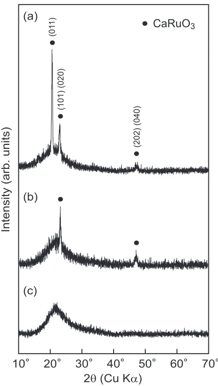
Fig. 1 XRD patterns of CRO thin films prepared at Tsub¼973K and
PO2¼0:13Pa fortdep¼3:6ks (a) and 7.2 ks (b), andTsub¼773K and
[image:1.595.319.532.306.683.2]The deposition was carried out in a high vacuum (UHV,
P¼106Pa) and in O
2at oxygen pressures (PO2) from 0.013
to 130 Pa. The substrate temperature (Tsub) was changed from room temperature to 1073 K. The films were approximately 50 and 100 nm in thickness at the deposition time (tdep) of 3.6 and 7.2 ks, respectively.
The crystal phase was studied by X-ray diffraction (XRD, Rigaku RAD-2C). The thickness was measured by a profilometer (Taylor-Hobson Talystep). Surface morphology was observed by a field-emission scanning electron micro-scope (FESEM, JEOL JSM-6500FT), and the composition was examined by energy dispersive X-ray spectroscopy (EDS) of FESEM. The binding energy was determined by X-ray photoelectron spectroscopy (XPS, Surface Science
SX100). Al K radiation (h¼1486:6eV) was employed
for the photoelectron excitation. The XPS spectra were fitted with Gaussian functions after a baseline correction. The XPS intensity ratio was derived from areas of convoluted peaks. The electrical resistivity was measured from 90 to 673 K by the van der Pauw method.
Fig. 2 Effect ofPO2on Lotgering factor of (100) (squares) and (111) plane (triangles) for CRO thin films prepared at Tsub¼973K for tdep¼3:6 (solid) and 7.2 ks (dashed).
Fig. 3 Effect ofPO2on the surface morphology of CRO thin films prepared atTsub¼973K andPO2¼130Pa (a), 67 Pa (b), 13 Pa (c), 0.13 Pa (d), 0.013 Pa (e) andP¼106Pa (f) fort
[image:2.595.63.274.70.272.2] [image:2.595.105.491.331.760.2]3. Results and Discussion
Figure 1 shows the XRD patterns of CRO thin films. Indexes (hkl) in Fig. 1 are denoted by orthorhombic notation. AtTsub¼973K andPO2¼13Pa, CRO thin films had a (011)
orientation attdep¼3:6ks (Fig. 1(a)), whereas (101)
(020)-oriented CRO thin films were obtained at tdep¼7:2ks
(Fig. 1(b)). CRO thin films prepared at Tsub ¼773K,
PO2¼13Pa and tdep¼7:2ks were amorphous and showed
only halo patterns of the quartz glass substrates (Fig. 1(c)).
Amorphous thin films were prepared at Tsub<773K for
tdep ¼7:2ks,Tsub <773K andTsub ¼1073K, andP¼106 Pa andPO2¼130Pa fortdep¼3:6ks. The (101) (020) and
(011) planes of orthorhombic CRO correspond to the (100) and (111) planes of pseudo-cubic CRO, respectively. Here-inafter, crystal planes are indexed using the pseudo-cubic notation. Figure 2 depicts the effect ofPO2on the (100) and
(111) orientation degree evaluated by Lotgering factor fð100Þ
and fð111Þ, respectively.12) fðHKLÞ for a (HKL) plane can be
given by eq. (1) and (2).
fðHKLÞ¼ ðPP0Þ=ð1P0Þ ð1Þ
P¼IðHKLÞ=IðhklÞ; ð2Þ
where P and P0 are calculated to an oriented and a
non-oriented specimen, respectively.Pis the XRD intensity ratio of a specific (HKL) plane to the summation of all (hkl) planes. XRD intensity (10<2 <80) of the (HKL) plane,IðHKLÞ, is determined by subtracting the halo diffraction of the quartz
glass substrate. I0 is calculated from the JCPDS-ICDD
card.13)With increasing P
O2, fð100Þ decreased whereas fð111Þ
increased independently of tdep. CRO thin films prepared at
PO2¼13Pa andtdep¼3:6ks had the highest degree of (111)
orientation.
Figure 3 shows the effect ofPO2 on the surface
morphol-ogy of CRO thin films prepared attdep¼3:6ks and Tsub¼
973K. Embedded rectangular-shaped CRO island grains 200
to 400 nm in size grew in the matrix at PO2¼130Pa
(Fig. 3(a)). While the size of these grains decreased at
PO2¼13Pa, their number increased and they were partially
connected (Fig. 3(b), 3(c)). In contrast, at PO2¼0:013Pa,
the size of the grains increased and they were deeply embedded in the matrix (Fig. 3(d), 3(e)). The CRO thin films
prepared at P¼106Pa consisted of elongated fine grains
30 nm in width and 100 nm in length (Fig. 3(f)). XRD results implied that the facets of rectangular-shaped island grains would be the pseudo-cubic (100) plane.
Figure 4 depicts the effect of Tsub on the surface
morphology of CRO thin films prepared at tdep¼3:6ks
and PO2¼13Pa. The CRO thin films prepared at Tsub<
573K showed a flat, smooth surface (Fig. 4(a)). Coarse
grains partially appeared at Tsub ¼873K (Fig. 4(b)). At
Tsub ¼1073K, rectangular-shaped island grains with slightly round-shaped edges were observed (Fig. 4(c)).
Figure 5 demonstrates the effect of Tsub on the surface
morphology of CRO thin films prepared attdep¼7:2ks and
PO2¼0:13and 13 Pa. With increasingTsub, the island grains
were enlarged and tended to separate independent ofPO2. At
PO2¼0:13Pa and Tsub ¼973K, and at PO2¼13Pa and
Tsub ¼873K, the densely connected grains were obtained
(Fig. 5(b), 5(d)).
Figures 6 and 7 demonstrate the effect of PO2 and Tsub,
respectively, on the Ca fraction (¼CCa=ðCCaþCRuÞ) of CRO thin films. The Ca fraction of CRO thin films increased
with increasing PO2. On the other hand, the Ca fraction
showed a minimum around Tsub ¼773K for tdep ¼3:6ks,
while it was almost constant betweenTsub ¼298and 973 K
and slightly increased atTsub¼1073K fortdep¼7:2ks. Figure 8 summarizes the EDS spot analysis of CRO thin
films prepared at PO2 ¼0:13Pa. The rectangular-shaped
grain and matrix had an almost stoichiometric composition at
Tsub ¼873K (Fig. 8(a)), whereas a significant increase in the
Ca fraction of the matrix was identified at Tsub ¼1073K
(Fig. 8(b)). The island grains showed a nearly stoichiometric composition independently ofTsub, while the Ca fraction of the matrix increased with increasingTsub.
Figure 9 demonstrates the Ru3dXPS spectra of CRO thin
films prepared at Tsub¼973K, P¼106Pa and tdep¼
3:6ks, and Tsub ¼973K, PO2¼0:13Pa and tdep ¼7:2ks.
The peak at 284.4 eV was assigned to carbon (C1s) from the
Fig. 4 Effect ofTsubon the surface morphology of CRO thin films prepared at PO2¼13Pa and Tsub¼773K (a), 873 K (b) and 1073 K (c) for
contaminated hydrocarbon adsorbed on the surface during exposure to air after deposition and in the XPS equipment. The Ru3dspin-orbit doublets for Ru4þ3d5=2and Ru4þ3d3=2
(281.0 and 286.0 eV, solid lines) with satellite peaks (282.5 and 289.2 eV, dashed lines), as well as the Ru03d
5=2and Ru0 3d3=2 peaks (279.7 and 284.8 eV, dashed-dotted lines) were
observed at P¼106Pa, T
sub ¼973K and tdep¼3:6ks (Fig. 9(a)). The satellite peaks could have been caused by a screening effect of Ru 3d core-electron.11,14) The Ru0 3d
peaks would imply the co-deposition of metallic Ru in the
CRO thin films prepared atP¼106Pa. AtP
O2¼0:13Pa,
Tsub ¼973K andtdep¼7:2ks, the CRO thin films had Ru3d spin-orbit doublets for Ru4þ3d
5=2and Ru4þ3d3=2(280.9 and
285.7 eV) with satellite peaks (282.7 and 287.4 eV) and a C
1s peak (284.4 eV) (Fig. 9(b)). These Ru 3d peaks had
characteristics in the carbon free polycrystalline RuO2 body
(280.8 and 285.0 eV with 282.6 and 286.3 eV)14)and the SRO thin films prepared by the present authors (281.0 and 285.6 eV with 282.8 and 287.6 eV).11)
Fig. 5 Effect ofTsubon the surface morphology of CRO thin films prepared atPO2¼0:13Pa andTsub¼873K (a), 973 K (b) and 1073 K (c), andPO2¼13Pa andTsub¼873K (d), 973 K (e) and 1073 K (f) fortdep¼7:2ks.
[image:4.595.106.491.69.499.2] [image:4.595.62.275.563.766.2]Figure 10 shows the O1sXPS spectra of CRO thin films prepared atTsub ¼973K,P¼106Pa andtdep¼3:6ks, and at Tsub¼973K, PO2¼0:13Pa and tdep¼7:2ks. Lower
binding energy at 528.8 and 528.6 eV (solid lines) and the higher binding energy at 531.2 and 530.7 eV (dashed lines) were observed in the O1sspectra (Fig. 10(a), (b)). The lower binding energy ranging from 529 to 530 eV, can be assigned to the binding state of the perovskite structure from XPS studies on (Ba, Sr)TiO3and CaTiO3.15–19)On the other hand, Fig. 7 Effect ofTsubon the Ca fraction of CRO thin films prepared at
variousPO2andtdep.
Fig. 9 Ru3dXPS spectra of CRO thin films prepared atTsub¼973K,
P¼106Pa andt
dep¼3:6ks (a), and atTsub¼973K,PO2¼0:13Pa and
tdep¼7:2ks (b).
[image:5.595.320.530.73.354.2] [image:5.595.101.498.453.759.2]the higher binding energy over 530 eV has been explained as
being a less negatively charged form,15) the C-O binding
state,16)the -OH binding state by water layer adhesion17,18) and the Ti2O3 phase or free O atoms.18)These effects might
be complicated, and it is usually too difficult to deconvolute into specific effects. Therefore, it is commonly analyzed by
separating O 1sspectra into perovskite and non-perovskite
components.11,18)The intensity of the non-perovskite
com-ponent decreased, while that of the perovskite comcom-ponent increased with increasingTsub andPO2.
Figure 11 shows the Ca2pXPS spectra of CRO thin films
prepared atTsub ¼973K,P¼106Pa andtdep¼3:6ks, and atTsub¼973K,PO2¼0:13Pa andtdep¼7:2ks. The Ca2p
spectra had spin-orbit doublets for Ca 2p3=2 and Ca 2p1=2
(345.2 and 348.3 eV, and 344.9 and 348.3 eV, solid lines) with higher binding energy states (346.8 and 350.3 eV, and 346.2 and 350.0 eV, dashed lines). Asamiet al.have reported
that the binding energies of Ca 2p3=2 were 346.3 and
347.7 eV, respectively, and that those of O1swere 529.4 and
531.3 eV for the perovskite CaTiO3 thin films annealed at
873 K for 7.2 ks in air and in a vacuum, respectively.20)They also reported that a CaO layer was formed on the top surface during the annealing in a vacuum due to partial decom-position of CaTiO3. A similar higher binding energy state has
been identified in SRO and BaRuO3 (BRO) thin films
prepared by the present authors.11)In the present study, a CaO layer or CaO-related different chemical state might be formed on the top surface of CRO thin films, and thus the lower and higher states of the Ca2pspectra can be separated into perovskite and non-perovskite components, respectively. With increasing Tsub and PO2, the intensities of the
non-perovskite component decreased whereas those of the
perovskite component increased, as in the case of the O 1s
spectra.
Figure 12 depicts the XPS intensity ratios of the perovskite component (SBEpero) to non-perovskite component (SBEnon-pero)
in the O 1s and Ca 2p XPS spectra for CRO thin films
prepared at PO2¼0:13Pa and 13 Pa for tdep¼7:2ks. The
CRO thin films prepared at Tsub¼298K were amorphous
and had no perovskite component in the Ca2pXPS spectra.
The perovskite components of O1sand Ca2pincreased with increasingTsubindependent ofPO2. The intensity ratios of the
perovskite component to the non-perovskite component in
the O 1s and Ca 2p spectra could be associated with the
crystallinity of CRO thin films.
Figure 13 shows the temperature dependence of electrical
conductivity () of CRO thin films from room temperature to
673 K. At tdep¼7:2ks, CRO thin films prepared at PO2¼ 0:13Pa and Tsub ¼973K, and at PO2¼13Pa and Tsub¼
873K exhibited metallic conduction, i.e., the decreased
with increasing temperature (Fig. 13(b), 13(e)), while the CRO thin films prepared in the present study commonly
showed semiconducting behavior, i.e., increased with
increasing temperature (Fig. 13(a), (c), (d), (g), (f)).
Figure 14 shows the temperature dependence of from
90 K to room temperature. Data from the literature on the polycrystalline CRO body (plot h),21)epitaxial CRO thin film (dashed i)22)and single crystal CRO (dotted g)1)are included in Fig. 14. These thin films of course had no change of
associated with the magnetic phase transition, in contrast
to SRO. Theof CRO thin films prepared atPO2¼0:13Pa
[image:6.595.320.531.71.357.2]and Tsub¼973K was almost the same as that of the
Fig. 10 O1sXPS spectra of CRO thin films prepared atTsub¼973K,
P¼106Pa andt
dep¼3:6ks (a), and atTsub¼973K,PO2¼0:13Pa and
[image:6.595.64.276.71.354.2]tdep¼7:2ks (b).
Fig. 11 Ca2pXPS spectra of CRO thin films prepared atTsub¼973K,
P¼106Pa andt
dep¼3:6ks (a), and atTsub¼973K,PO2¼0:13Pa and
polycrystalline CRO body and epitaxial CRO thin film (Fig. 14(e)).
Figure 15 demonstrates the effects of Tsub on of CRO
thin films prepared at variousPO2fortdep¼7:2ks. Open and
filled circles indicate metallic and semi-conducting behavior,
respectively. The CRO thin films with <104Sm1
showed semiconducting behavior. Hyunet al. reported that
the electrical conduction behavior changed from metallic to semiconducting as the thickness of epitaxial CRO thin films decreased below 60 nm.10)In the present study, the separated island grains grew on the CRO thin films. Therefore, the effective thickness for electron conduction of the CRO thin films,i.e., the thickness of matrix, might be insufficient for
metallic conduction. Moreover, at Tsub ¼1073K, the
furthermore decreased with decreasing Ru content of matrix.
On the other hand, CRO thin films prepared atPO2¼0:13Pa
andTsub ¼973K, and atPO2¼13Pa andTsub ¼873K had a
continuous surface of connected grains and thus exhibited metallic conduction. The optimum deposition condition for
the highest was in agreement with that of the highest
SBEpero=SBEnon-pero shown in Fig. 12.
4. Conclusions
CRO thin films were prepared on quartz glass substrates by laser ablation under various conditions. The orientation of CRO thin films changed from (100) to (111) with increasing
PO2. Rectangular-shaped CRO island grains grew at
[image:7.595.319.533.71.274.2]Fig. 12 Effect of PO2 on the XPS O 1s and Ca 2p BEpero=BEnon-pero intensity ratio for CRO thin films prepared at variousTsubandPO2¼13Pa (circle) and 0.13 Pa (square) fortdep¼7:2ks.
Fig. 13 Temperature dependence of electrical conductivity at high temper-ature for CRO thin films prepared atPO2¼13Pa andTsub¼1073K (a), 873 K (b) and 773 K (c), and atPO2¼0:13Pa andTsub¼973K (d), 873 K
[image:7.595.62.279.336.537.2](e) and 773 K (f) fortdep¼7:2ks. Fig. 15 Effects of Tsub on electrical conductivity of CRO thin films prepared at variousPO2fortdep¼7:2ks. Open and filled circles indicate metallic and semi-conducting behavior, respectively.
Fig. 14 Temperature dependence of electrical conductivity at a low temperature for CRO thin films prepared at PO2¼13Pa and
Tsub¼1073K (a), 873 K (b) and 773 K (c), and atPO2¼0:13Pa and
[image:7.595.318.532.366.567.2]Tsub >873K. CRO thin films with connected island grains were obtained at 873K<Tsub<973K. Separated island
grains with round-shaped edges were observed at Tsub¼
1073K. While the island grains had an almost stoichiometric
composition independently of Tsub, the Ca fraction of the
matrix increased with increasing Tsub. Both perovskite
components for O 1s and Ca 2p in XPS spectra increased
with increasingTsubindependent ofPO2. CRO thin films with
<104Sm1showed semiconducting behavior. CRO thin
films prepared atPO2¼0:13Pa andTsub¼973K exhibited
the highestof 1.5 105Sm1 at room temperature with
metallic conduction.
Acknowledgements
This research was supported in part by the 21st Century COE Program of Tohoku University, and by the Asian CORE Program, Japan Society for the Promotion of Science (JSPS). We are grateful to N. Ohtsu, Institute for Materials Research, for XPS measurement, and to Y. Hayasaka and E. Aoyagi, Institute for Materials Research, for FESEM observation. This research was financially supported in part by Furuya Metal Co., Ltd. and Lonmin Plc.
REFERENCES
1) R. J. Bouchard and J. L. Gillson: Mater. Res. Bull.7(1972) 873–878. 2) X. G. Tang, H. Y. Tian, J. Wang, K. H. Wong and H. L. W. Chan: Appl.
Phys. Lett.89(2006) 142911.
3) C. B. Eom, R. B. Van Dover, J. M. Phillips, D. J. Werder, J. H. Marshall, C. H. Chen, R. J. Cavaand, R. M. Flemingand and D. K. Fork: Appl. Phys. Lett.63(1993) 2570–2572.
4) K. Char, M. S. Colclough, T. H. Geballe and K. E. Myers: Appl. Phys. Lett.62(1993) 196–198.
5) S. Kamal, D. M. Kim, C. B. Eom and J. S. Dodge: Phys. Rev. B74
(2006) 165115.
6) H. Funakubo, T. Oikawa, N. Higashi and K. Saito: J. Crystal Growth
235(2002) 401–406.
7) S. Yamada, N. Fukuoka, T. Taniguchi, T. C. Ozawa, Y. Nagata, T. Uchida and H. Samata: Thin Solid Films478(2005) 1–5.
8) F. Ricci, M. F. Bevilacqua, F. M. Granozio and U. S. di Uccio: Phys. Rev. B65(2002) 155428.
9) L. Klein, L. Antognazza, T. H. Geballe, M. R. Beasly and A. Kapitulnik: Physica B259–261(1999) 431–432.
10) S. Hyun, J. H. Cho, A. Kim, J. Kim, T. Kim and K. Char: Appl. Phys. Lett.80(2002) 1574–1576.
11) A. Ito, H. Masumoto and T. Goto: Mater. Trans.47(2007) 2808–2814. 12) F. K. Lotgering: J. Inorg. Nucl. Chem.9(1959) 113–123.
13) JCPDS #82-1476.
14) P. A. Cox, J. B. Goodenough, P. J. Tavener, D. Telles and R. G. Egdell: J. Solid State Chem.62(1986) 360–370.
15) S. A. Nasser: Appl. Surf. Sci.157(2000) 14–22.
16) M. Viviani, M. T. Buscaglia, P. Nanni, R. Parodi, G. Gemme and A. Dacca: J. Euro. Ceram. Soc.19(1999) 1047–1051.
17) A. L. Morales-Cruz, F. W. Van Keuls, F. A. Miranda and C. R. Cabrera: Appl. Surf. Sci.252(2005) 981–995.
18) J. X. Liao, C. R. Yang, J. H. Zhang, C. L. Fu, H. W. Chen and W. J. Leng: Appl. Surf. Sci.252(2005) 7407–7414.
19) S. Kacˇiulis, G. Mattogno, L. Pandolfi, M. Cavalli, G. Gnappi and A. Montenero: Appl. Surf. Sci.151(1999) 1–5.
20) K. Asami, N. Ohtsu, K. Saito and T. Hanawa: Surf. Coat. Technol.200
(2005) 1005–1008.
21) N. Keawprak, R. Tu and T. Goto: Mater. Trans.48(2007) 1529–1533. 22) A. Ito, H. Masumoto and T. Goto: Key Eng. Mater.352(2007) 315–