Effect of Surface Contamination on Solid-State Bondability
of Sn-Ag-Cu Bumps in Ambient Air
Ying-Hui Wang
*and Tadatomo Suga
Department of Precision Engineering, School of Engineering, The University of Tokyo, Tokyo 113-8656, Japan
Two solid-state bonding methods, thermocompression bonding (TCB) and surface activated bonding (SAB), were used for studying the effect of surface contamination on the bonding of Sn-Ag-Cu bumps in ambient air. The surface contamination was analyzed by X-ray photoelectron spectroscopy. Correlated to the surface contamination, the influence of Ar-plasma pretreatment time as well as the air exposure time on the shear strength was investigated in SAB process. The bonding of Sn-Ag-Cu bumps was achieved at 25–200C benefiting from dispersing the surface contamination. With an Ar-plasma activation process prior to the assembly under a low-vacuum background, the carbon contaminants on the bump surfaces in SAB process was removed, and the required bonding pressure or temperature to achieve a high shear strength and bond yield is lower than that in TCB process. [doi:10.2320/matertrans.MF200804]
(Received January 8, 2008; Accepted March 31, 2008; Published May 21, 2008)
Keywords: surface contamination, thermocompression bonding, surface activated bonding, tin-silver-copper bump
1. Introduction
Sn-Ag-Cu alloys, with a ternary eutectic melting point at 217C, become the main stream of lead-free alloys in electronic packaging field because of better reliability and solderability than other alternatives.1–3) The conventional
bonding process of Sn-Ag-Cu bumps is reflow soldering, which exists several problems in high density packaging. First, it requires complex reflow profiles and long time.4) Secondly, the bonding temperature of Sn-Ag-Cu solders should be higher than that of conventional Pb-Sn solders.5) The thermal stresses result in not only misalignment but also poor reliability.6)In order to prevent oxidation of the alloys at
high temperatures, fluxes and a special environment with N2 or H2 gas, are used in the soldering process. However, the flux residues are difficult to be removed from the fine-pitch bump interconnections, and also are responsible for void formation.4)In addition, constructing an environment system
makes the assembly equipment complex and increases the cost. Furthermore, failures of the interconnections using low-profile Sn-Ag-Cu solder bumps with high percent IMCs inevitably become a bottleneck in the development of high density packaging to miniaturize the size of solder bumps.
In contrast to the conventional reflow soldering process, an approach of solid-state bonding is proposed to accomplish the low-temperature low-cost fluxless bonding for Sn-Ag-Cu bumps. However, little work has been conducted to examine the bonding feasibility of Sn-Ag-Cu bumps in solid state in ambient air. Thermocompression bonding (TCB) and surface activated bonding (SAB) are solid-state bonding processes. TCB is an assembly method to get interconnections using thermal heating and pressure compression, which is widely used in Au-to-Au bonding.7) SAB method is based on the
very strong metal or covalent bonding energy between two atomic clean surfaces.8)The clean surfaces can be obtained
by performing dry process such as argon fast atom beam or ion beam in high vacuum. In the previous investigations, various metals and their alloys as well as the combinations to some ceramics and semiconductors have been bonded at
room temperature in high vacuum.8–11)The bonding of
Sn-Ag-Cu bumps has also achieved in ambient air and be found critical to air exposure time.12) However, the bondability
of Sn-Ag-Cu bumps activated in low vacuum, the critical process parameters, and the required bonding pressure and temperature compared with those using the TCB method, which correlate with surface contamination, are not clear.
In the present study, argon radio frequency plasma (Ar RF plasma) under a low-vacuum background was selected as the surface activation process for bonding Sn-Ag-Cu bumps in SAB process. The difference of the surfaces without and with Ar-plasma pretreatment was studied. The critical pretreat-ment time and air exposure time were investigated in SAB process. The influence of surface contamination on the required bonding pressure and temperature to bonding Sn-Ag-Cu bumps was studied using both of the TCB and SAB methods at 25–200C in ambient air.
2. Experimental Details
2.1 Analysis procedure for surface contamination Surface contamination influences the bonding behavior. In order to know the surface conditions in TCB and SAB processes, the surface analysis was performed using X-ray photoelectron spectroscopy (XPS, JEOL-JPS-9200T). Since XPS analysis is limited in micro-areas13)and the contami-nation behaviors of Sn-Ag-Cu and Sn-Ag are similar,12–14)
Sn-2.0Ag (mass%) alloy films with the size in millimeter scale were prepared for the analysis corresponding to the bonding experiments of bumps. The Sn-Ag film was fabricated in 5-mm-square shape with a thickness of 18mm on a 10-mm-square Si substrate. The measurement was carried out using Mg-Kradiation of the energy of 1253.6 eV with 10 kV accelerating voltage and 10 mA emission current. An additional chamber of the XPS tool was equipped for Ar-plasma pretreatment. It makes the in-stu analysis available for the activated surfaces pretreated by Ar-plasma under a low-vacuum background before air exposure. The surface without pretreatment corresponds to the one bonding in TCB process, and the activated surface after air exposure corre-sponds to the one bonding in SAB process.
*Graduate Student, The University of Tokyo
2.2 Bonding procedure
Sn-3.0Ag-0.5Cu (mass%) bumps were used in the bond-ing. The numbers in the alloy denote the composition in mass%. There are 288 electroplated bumps on chips in correspondence with the same number and structure bumps on substrates. The bump size is 40mmin diameter, and the pitch size is 60mm. In order to enlarge contact areas during bonding, a planarization technique was used to flatten the Sn-Ag-Cu bump surfaces. The planarization technique is an ultra-precision cutting process using a single-crystal diamond cutter. It may reduce the bump height variation and surface roughness of bumps.15)In this study, the height of bumps is
cut to as thin as 3.5mm, and the surface roughness (rms) is around 10 nm after the planarization process. The scanning electron microscope (SEM) image of the Sn-Ag-Cu bumps is shown in Fig. 1. The under-bump-metallization (UBM) is Ni-P and the thickness is 4.5mm. The Sn-Ag-Cu alloy reacted with UBM to form the intermetallic compounds (IMCs) of Ni3Sn4, therefore the remaining Sn-Ag-Cu alloys on top of the bumps was less than 3.5mm. The assembly of such low-profile bumps is a challenge in the conventional reflow soldering process. Several daisy chains were designed for checking the electrical resistance.
The bonding experiments were carried out using a submicron flip-chip bonder. The accuracy of mounting and parallelism of this bonder may reach the submicron level.16)
There were five steps in the bonding procedure: preplacing, samples transfer, alignment, bonding and discharge. First, the samples were placed into the pretreatment chamber of the bonder (TCB: without any pretreatment; SAB: Ar RF plasma pretreatment (100 W) for a specified time); then the samples were transferred into the bonding chamber; alignment was performed; after alignment, the samples were bonded together with a certain bonding force for 30 s at a specified temperature; finally, the bonded sample was returned back to the pretreatment chamber. In SAB process, the whole process was carried out in ambient air except the step of Ar-plasma pretreatment which was performed under a vacuum background of 5–10 Pa.
2.3 Evaluation procedure
The electrical resistance and die shear tests were per-formed to check the electrical and mechanical characteristics of the bonded samples. The bond interface was observed using an optical microscope.
3. Results and Discussion
3.1 Analysis of surface contamination
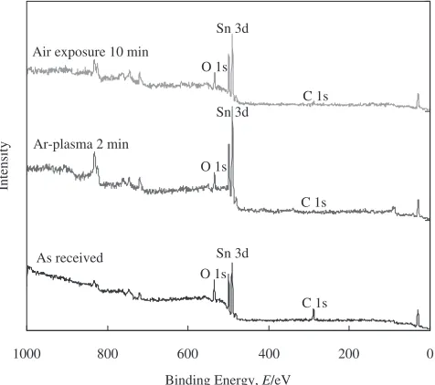
Surface contamination of lead-free alloys is composed by carbon contaminants and oxides, which may influence the bonding behavior. In order to know the conditions of surface contamination on the bond pair in TCB and SAB processes, the surface analysis was performed by XPS. Figure 2 shows the XPS wide scan spectra of the Sn-Ag surface as received, after Ar-plasma pretreatment for 2 min, and after air exposure for 10 min. Without Ar-plasma pretreatment, carbon and oxygen peaks were obviously observed on the surface, which was the surface condition in TCB process. After Ar-plasma pretreatment for 2 min, the carbon peak disappeared from the surface, but the oxygen peak still appeared after Ar-plasma pretreatment under a low-vacuum background of 5–10 Pa. The etching rate of it irradiated by Ar-plasma is around 0.2 nm/s. The etching depth after 2-min-irradiation was more than 20 nm, which was larger than the total thickness of carbon contaminants and oxides of 12 nm.12) The residual oxygen gas in the
low-vacuum atmosphere is assumed the reason of oxide remaining. With the exposure time extending, both of the oxide and carbon contaminants grew slowly and the growth of them followed a logarithmic rate law. Only a little carbon peak appeared after air exposure for 10 min. The surface condition in this case corresponds to the one in SAB process. The surface contamination in SAB and TCB processes mainly appears difference in carbon contami-nants.
60
µ
m
40
µ
m
Fig. 1 SEM image of the Sn-Ag-Cu bumps.
0 200
400 600
800 1000
Binding Energy, E/eV
Intensity
O 1s
C 1s Sn 3d
As received
O 1s
C 1s Sn 3d
Ar-plasma 2 min
O 1s
C 1s Sn 3d
Air exposure 10 min
[image:2.595.309.547.73.284.2] [image:2.595.49.290.73.262.2]3.2 Solid-state bonding of Sn-Ag-Cu bumps
In order to know the effect of surface contamination on the bonding of the Sn-Ag-Cu bumps, the influence of Ar-plasma pretreatment and air exposure time on the shear strength was investigated. The shear strength of the Sn-Ag-Cu bumps bonded with different Ar-plasma pretreatment time was shown in Fig. 3. The samples were bonded at 100C under the bonding pressure of 200 and 250 MPa after Ar-plasma pretreatment for 0–180 s and air exposure within 3–30 min. Under the bonding pressure of 200 MPa, the shear strength increased dramatically when the pretreatment time reached 10 s. The etching depth of Ar-plasma pretreatment is similar to that in the XPS instrument, and a 10-s pretreatment caused an etching depth of 2 nm to remove the carbon contaminants from the sample surfaces. Since oxides existed after Ar-plasma pretreatment under the low-vacuum background and did not grow quickly after air exposure, the addition of carbon contaminants with the oxides seems to have a great influence on the bonding in this case. The influence of air exposure time on the shear strength was shown in Fig. 4. The
samples were pretreated by Ar-plasma for 2 min and bonded at 100C under the bonding pressure of 200 MPa. The shear strength fell dramatically when the exposure time reached around 120 min. The growth of carbon contaminants and oxides influenced the bonding behavior. Therefore, the thickness of them is the controlling factor. However, such a critical time was not detected under the bonding pressure of 250 MPa. Under this bonding pressure, the shear strength reached around 20 MPa even though the sample surfaces were not pretreated by Ar-plasma and did not increased obviously in this case, as shown in Fig. 3(a). The surface contamination has little effect on the bonding under a large bonding pressure.
The compared bond yield and shear strength of the samples bonded by the TCB and SAB methods are shown in Table 1 and Fig. 5, respectively. The samples were bonded at 100C under the bonding pressure of 150–335 MPa. The Ar-plasma pretreatment time and air exposure time in the case of SAB process were 2 min and 3–30 min, respectively. The bond yield in the case of TCB was lower than that of SAB especially under 150–225 MPa. In SAB, although the shear strength was not large, the bump chains achieved the electrical connections. However, in TCB, a high bond yield cannot be achieved using a bonding pressure less than 250 MPa. The shear strength in TCB was near to zero and much smaller than that in SAB at the beginning, and increased to the maximum level when the bonding force reached 250 MPa. It seems that a bonding pressure less than 250 MPa is not enough to disperse the initial surface 0
5 10 15 20 25 30 35
0
200 MPa 250 MPa
Shear Strength,
σ
/
MPa
Ar-Plasma Pretreatment Time, t/s
(a)
200 150
100 50
0 5 10 15 20 25 30
1
Shear Strength,
σ
/
MPa
Ar-Plasma Pretreatment Time, t/s
(b)
1000 100
10
Fig. 3 Influence of Ar-plasma pretreatment time on shear strength of the samples bonded at 100C by the SAB method with the air exposure time within 3–30 min: (a) under the bonding pressure of 200 and 250 MPa and (b) under the bonding pressure of 200 MPa.
0 5 10 15 20 25 30
1
Shear Strength,
σ
/
MPa
Air Exposure Time, t/min
10000 1000
100 10
[image:3.595.54.284.62.482.2]Fig. 4 Influence of air exposure time on shear strength of the samples bonded at 100C under the bonding pressure of 200 MPa by the SAB method.
Table 1 Bond yields of the connected Sn-Ag-Cu bumps by the TCB and SAB methods at 100C.
Bonding Pressure (MPa)
Bond Yield (%) by the TCB Method
Bond Yield (%) by the SAB Method
150 0 35–100
200 0–50 100
225 25–75 100
250 50–100 100
[image:3.595.309.546.72.244.2] [image:3.595.305.549.329.422.2]contamination on top of the bump surfaces at this condition. In SAB, the shear strength increased followed with the bonding pressure at the beginning, and kept to the similar values when the bonding pressure reached 225 MPa. The effect of bonding pressure on the bonding can probably be explained as the resulting of the enhancement of the plastic deformation underlying the bumps, which breaks up the surface contaminants and promotes their granulation to decrease the energy of the interface expanded by this break up. The actual contact areas of the alloys are consequently enlarged during the crush and migration of contamination particles induced by the plastic flow in the alloys. Previous studies12,14) show that the initial thickness of the surface
contamination on lead-free alloys is around 5–20 nm. The softness of the Sn-Ag-Cu alloys and thin surface contami-nation make two alloy surfaces into actual contact under large deformation.
Figure 6 shows the cross-sectional optical image of the Sn-Ag-Cu bumps bonded at 100C under the bonding pressure of 200 MPa by the SAB method. No void was observed in the bond interface even though less than 3.5mm thick Sn-Ag-Cu alloy remained on top of the bumps. These fractures after die shear test occurred inside of the bumps. Ag3Sn and Ni3Sn4 were detected on the fractured surfaces. High percent of the IMCs on the bonded bumps may degrade the mechanical properties because of their brittleness and result in the fractures occurred only inside of bumps.17)
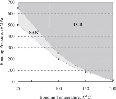
The required bonding pressure and temperature for bonding the Sn-Ag-Cu bumps by the TCB and SAB methods were evaluated at 25–200C. These values were determined when the shear strength was larger than 10 MPa and the bond yield reached 100%, as shown in Fig. 7. With the elevation of the bonding temperature, the required bonding pressure becomes smaller, and the gap between TCB and SAB is also reduced. Heating can soften the Sn-Ag-Cu bumps and accelerate the diffusion of solder alloys. Not only contact deformation, but also diffusion is considered to the contri-bution of breaking up the surface contaminants. When the
bonding temperature or pressure is fixed, the required bonding pressure or temperature in SAB is smaller than that in TCB. The solid-state bonding of the Sn-Ag-Cu bumps is mainly benefits from dispersing surface contamination. When the Ar-plasma activation process is applied to the bonding surfaces prior to the assembly, the surface contam-ination in SAB is less than that in TCB. Therefore, the SAB method is very helpful to reduce the required bonding pressure or temperature, especially at low temperatures or pressures compared with those necessary for the TCB method.
4. Conclusion
The bonding of the Sn-Ag-Cu bumps was achieved at 25– 200C by the TCB and SAB methods benefiting from dispersing the surface contamination. The surface contami-nation in SAB process, which pretreated by Ar-plasma under 0
5 10 15 20 25 30 35 40
100
SAB TCB
Shear Strength,
σ
/
MPa
Bonding Pressure, σ/MPa
400 350 300 250 200 150
Fig. 5 Comparison of shear strength achieved by the TCB and SAB methods at 100C.
40µm
60µm
10µm Si substrate
Si chip
Bond interface of Sn-Ag-Cu bumps
Ni-P
Ni-P Ni3Sn4
Fig. 6 Cross-sectional optical image of the Sn-Ag-Cu bumps bonded at 100C under the bonding pressure of 200 MPa by the SAB method.
0 100 200 300 400 500 600 700
25 100 150 200
σ
/
MPa
Bonding Pressure,
TCB
SAB
Bonding Temperature, T/ °C
[image:4.595.308.546.73.267.2] [image:4.595.52.289.73.284.2] [image:4.595.309.546.320.523.2]the low-vacuum background, is mainly appeared in the removal of carbon contaminants. A critical pretreatment time as well as air exposure time is detected in the bonding under 200 MPa at 100C due to the existence of surface contamination. With larger deformation, those critical values are not detected in the bonding under 250 MPa. The SAB method can reduces the required bonding pressure or temperature, especially at low temperatures or pressures compared with the TCB method.
Acknowledgments
The authors would like to express sincere thanks to Micro-Electronics Materials Laboratory of Fujitsu Laboratories Ltd. Japan for the cooperation, and Mr. M. Mizukoshi and Mr. T. Akamatsu are specially appreciated for the valuable advice.
REFERENCES
1) K. Suganuma: Curr. Opin. Solid State Mater. Sci.5(2002) 55–64. 2) M. E. Loomans and M. E. Fine: Metal. Mater. Trans. A31(2000)
1155–1162.
3) M. O. Alam, Y. C. Chan and K. N. Tu: J. Appl. Phys. 94(2003) 7904–7909.
4) C. Davoine, M. Fendler, F. Marion, C. Louis and R. Fortunier: Proc. 56th IEEE-ECTC Conference, (2006) pp. 24–28.
5) M. Abtew and G. Selvaduray: Mater. Sci. Eng. R27(2000) 95–141. 6) K. Zeng and K. N. Tu: Mater. Sci. Eng. R38(2002) 55–105. 7) B. K. Kurman and S. G. Mita: Proc. 42nd IEEE-ECTC Conference,
(1992) pp. 883–889.
8) T. Suga, Y. Takahashi, H. Takagi, B. Gibbesch and G. Elssner: Acta Metall. Mater.40(Suppl.) (1992) S133–S137.
9) H. Takagi, R. Maeda, T. R. Chung, N. Hosoda and T. Suga: Jpn. J. Appl. Phys.37(1998) 4197–4203.
10) N. Hosoda, Y. Kyogoku and T. Suga: J. Mater. Sci.33(1998) 253–258. 11) Q. Wang, Z. H. Xu, M. R. Howlader, T. Itoh and T. Suga: Proc. 52nd
IEEE-ECTC Conference (2002) pp. 915–919.
12) Y. H. Wang, R. H. Matiar, K. Nishida, T. Kimura and T. Suga: Mater. Trans.46(2005) 2431–2436.
13) Y. Iijima: JEOL News38(2003) 46–50.
14) T. Suga, H. Ozaki and H. Ozawa: IEEE, Proc. 56th IEEE-ECTC Conference, (2006) pp. 1223–1226.
15) M. Mizukoshi: Proc. SEMICON Technology Symposium, Japan, (2004) 825–826.
16) Y. H. Wang, K. Nishida, M. Hutter, T. Kimura and T. Suga: Jpn. J. Appl. Phys.46(2007) 1961–1967.