Evaluations of Mechanical Properties of Electrodeposited Nickel Film by Using
Micro-Testing Method
*1Takashi Nagoshi
1,2,*2, Tso-Fu Mark Chang
2and Masato Sone
21Advanced Manufacturing Research Institute, National Institute of Advanced Industrial, Science and Technology, Tsukuba 305–8564, Japan
2Institute of Innovative Research, Tokyo Institute of Technology, Yokohama 226–8503, Japan
Compression and tensile testing of electrodeposited nickel films with micro-sized specimens were reviewed. Preparation of micro-speci-mens without the tapering was realized by the micro-specimen fabrication method developed in our group. Accurate micro-testing method with precisely-shaped specimens is needed to reveal micro-mechanical properties of electrodeposited metals. The micro-testing on nanocrystalline nickel plated by an electrodeposition method with supercritical carbon dioxide showed remarkably high strength, and the strength increased with a decrease in the specimen size. The results indicated grain boundary mediated deformation of the electrodeposited nanocrystalline nickel.
[doi:10.2320/matertrans.MG201622]
(Received March 18, 2016; Accepted September 1, 2016; Published November 25, 2016)
Keywords: micro-testing, electrodeposition, nanocrystalline nickel
1. Introduction
Evaluations of mechanical properties using micro-sized specimens have received a great amount of interest for the micro-components used in the micro-electro-mechanical sys-tems (MEMS). Mechanical properties of materials are strong-ly dependent on the microstructures, such as, grain boundar-ies, crystal orientation, or dislocation densities. In addition, the effect of specimen size emerges when the size comes be-low several tens of micrometers1–3). Precise evaluation of me-chanical properties of the micro-components is necessary for design of new MEMS devices. Therefore, micro-specimens having precise dimensions and sophisticated testing method-ologies are needed for the evaluation of the micro-mechanical properties.
Electrodeposited nickel films, which have high strength and resistance to corrosion or abrasion, are often used in elec-tronic industry. By integrating the electrodeposition tech-nique with the lithography process, three dimensional com-ponents can be rapidly fabricated, and the production method is widely applied in the manufacturing process of MEMS components. Evaluating mechanical properties of the electro-deposited nickel films in micro-scale is important to deter-mine the reliability and the durability of the components used in MEMS. This paper summarizes reports on the mechanical property evaluations of electrodeposited nickel films using a micro-testing method developed in our group.
2. Micro-Testing Methods
Focused ion beam (FIB) machining is widely used to fabri-cate micro-sized specimens. Specific portion of the specimen can be milled away by focused Ga ion beam, which enables versatile machining of the sample. However, the milled sur-face could be tilted from one to two degrees with respect to
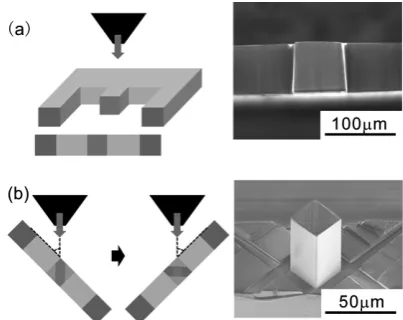
the beam direction. Because of this, the specimens fabricated by FIB machining would be tapered, and further mechanical testing would be unreliable4). In order to solve this problem, Uchic et. al reported a lathe milling method to fabricate non-tapered uniform cylindrical pillars. This method used an automated system involving series of sidewall milling and ro-tation while the specimen tilted several degrees with respect to the beam direction. The automated system including image correlation procedures and stage manipulation steps devel-oped by Shade and Uchic5). On the other hand, the fabrication method developed in our group applied two Ga ion beam di-rections perpendicular to axes of the pillar to fabricate non-ta-pered pillars with square cross-section6,7). The fabrication procedures are as follows. At first, edge of the mechanically polished thin plates with thickness of around 50 μm was FIB milled in two square areas to leave a square-pillar-shaped portion as shown in Fig. 1(a). The pillar was then whittled down to a smaller one using the beam with 45 degrees off from the first milling process Fig. 1(b). All sidewalls and top surface of the pillar were further milled with the beam tilted for several degrees to ensure precise dimensions of the pillar
*1
This Paper was Originally Published in Japanese in J. Japan Inst. Met. Mater. 80 (2016) 7–12.
*2
Corresponding author, E-mail: [email protected]
Fig. 1 Schematic and corresponded SEM images in the pillar fabrication process.
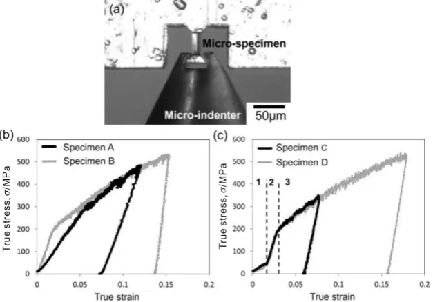
[image:1.595.324.526.599.759.2]ten not supported. Therefore, a universal micro-testing ma-chine should be specially made and customized for various testing modes and sizes of the specimen. An illustration of the micro-testing machine developed in our group is shown in Fig. 3. The machine is equipped with an X-Y-Z stage to lo-cate the specimen and a single axis actuator to load the spec-imen, which enable the testing of compression, tensile and bending in a single system. The load capacity and the sensi-tivity can be modified by selecting different load cell.
3. Tensile Testing of the Single Crystal Nickel
Consistency of the mechanical property evaluations to the bulky material testing, especially for the deformation
behav-results were shown in Fig. 4 as stress strain curves. All the tests stopped and unloaded before the onset of necking, thus, no specimens reached fracture. Table 1 shows the top six highest Schmid factors for orientations obtained from elec-tron backscattered diffraction measurement. From the report-ed resolvreport-ed critical shear stress (CRSS) of bulk nickel (3.24– 7.35 MPa11)) and the highest Schmid factor of the pillar, the yield stresses are estimated to be 9.81–22.27 MPa and 7.36– 1.05 MPa for samples with 〈111〉 and 〈223〉 orientations,
re-Fig. 2 Fabricated micro-tensile specimen observed in SEM. Fig. 3 Micro-mechanical test systems developed in our lab.
[image:2.595.314.540.302.496.2] [image:2.595.78.259.363.497.2] [image:2.595.142.456.543.762.2]spectively. Although the observed yield stresses are not reli-able while the input loads are far smaller than the maximum load in this case, the estimated yield stresses are comparable to the observed yield stress of 6.3–10.5 MPa. The tensile re-sults of the specimen with 〈223〉 orientation showed the typi-cal stress-strain curve of fcc single crystal sample, which ex-hibits 3 stages, the easy glide, the linear hardening, and the parabolic hardening stages. On the other hand, the easy glide regime was absent from the tensile test of the specimen with
〈111〉 orientation. In the easy glide regime, dislocations could freely glide on a single slip plane that has a high Schmid fac-tor. However, the specimen with 〈111〉 orientation had several slip planes with a high Schmid factor, thus, the movement of dislocations blocked each other on different slip planes even in early stage of the deformation. The deformation behavior observed in the micro-tensile tests well reflected the orienta-tions of the samples and showed the well-known mechanical behaviors of single crystal fcc metals. The results indicate our micro-tensile testing is capable to precisely evaluate mechan-ical properties of anisotropic materials for MEMS applica-tions.
4. Evaluations of Mechanical Properties of Nanocrystal-line Nickel by Micro-Compression and Micro-Tensile Tests
4.1 Electrodeposition of nanocrystalline nickel using su-percritical CO2 emulsion
Conventional electroplating (CONV) of nickel generally produce columnar microstructures with anisotropic proper-ties in strength and stiffness. Anisotropic properproper-ties could rise difficulties for the application as MEMS components12,13). On the other hand, co-produced hydrogen gas bubbles in the electroplating could be entrapped into the film to form
pin-holes or cause patterning-related problems. These failures occurred in the deposition process are critical issues in fabri-cations of MEMS components.
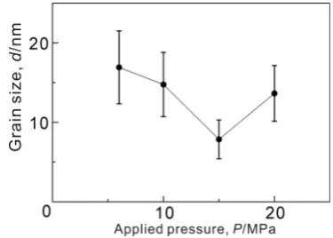
[image:3.595.139.457.69.170.2]Electroplating with supercritical CO2 emulsion (ESCE) is an electrodeposition method using an emulsified electrolyte formed by mixing supercritical CO2, surfactants, and an aqueous electrolyte14,15). In this electrodeposition method, co-produced hydrogen gas bubbles are immediately removed away from the cathode to give smooth electrodeposited films with less pinholes. Moreover, as schematically shown in Fig. 5, the electroplating reaction is interrupted on specific surface where the dispersed CO2 micelles are in contact with the cathode, and the reaction eventually resumes when the micelles leave the surface. These features are named periodic plating characteristics (PPC) and suggested to give the grain refinement effect16,17). Grain size of the film prepared by the ESCE varied with the reaction pressure as shown in Fig. 6. A minimum grain size of 6 nm was obtained when 15 MPa was used. Results of elemental analysis using glow discharge op-tical emission spectroscopy are shown in Table 2. The ESCE film contained higher carbon impurities than the film deposit-ed by the CONV using an electrolyte with the same surfac-tant. The carbon would be co-deposited from the dissolved CO2 as S.T. Chung and W.T. Tsai18) reported in electrodepo-sition with supercritical CO2. Smaller grain size observed from the film with a high carbon content indicates the co-de-posited carbon would contributed to the grain refinement. TEM images of the nickel film deposited at 15 MPa are shown in Fig. 7. Both observations from in-plane and cross section showed equi-axial grains with ring shaped diffraction image, thus, the isotropic mechanical properties is expected. On the other hand, no intermetallic compound such as nickel
Table 1 Slip systems on single crystal samples with the top six highest Schmid factors.
Loading axis: 〈111〉 Loading axis: 〈223〉 Slip system Schmid factor Slip system Schmid factor [110](−11–1) 0.33 [101](−1–11) 0.44
[0–11](111) 0.32 [1–10](11–1) 0.43 [−101](1–11) 0.30 [−101](1–11) 0.35 [−101](111) 0.28 [110](−11–1) 0.35 [0–11](−111) 0.19 [0–11](111) 0.09 [110](−111) 0.19 [0–11](−111) 0.08
Fig. 5 Schematics of reaction model in periodic plating characteristics (PPC) effect: (a) nickel nucleus generated on substrate and (b) nickel nuclei stopped growing when dispersed CO2 engulfed them.
[image:3.595.331.519.226.360.2] [image:3.595.46.292.251.354.2]height and 20 μm on a side length, and tensile specimen C and D both had 50 μm of gauge length and 10 μm on a side length were fabricated. Test results of each specimens are shown in Fig. 86,9). The maximum stresses observed in the compression and the tensile test were 3.5 and 3.0 GPa, re-spectively. As shown in Fig. 9, specimen C after the tensile
deformed metallic materials19) and suggested to be caused by reduced grain size. Dislocations could not move in small grains, and therefore, the work hardening was suppressed. As a consequence, the plastic instability condition was reached in early stages of the deformation. The flow stress was higher in the compression test than tensile test, and the ratio of the yield and maximum stresses obtained from the compression test to the stresses obtained from the tensile test were 1.13 and 1.2, respectively. The deformations of polycrystalline metallic materials which deform via dislocation activity have direct influence on the shear stress applied and not on the static pressure20). On the other hand, for materials deformed by grain boundary mediated route, such as grain boundary sliding and grain boundary dislocation emission, the static
Fig. 7 TEM bright field image of electrodeposited nickel, inset shows dif-fraction image.
Fig. 8 Results of micro-testing on electrodeposited nanocrystalline nickel. (a) Compression test and (b) tensile test as engineering stress-engineering strain curves.
[image:4.595.46.291.290.404.2]Fig. 9 SEM images of deformed sample. (a) Sample A, (b) sample C, (c) sample D, and (d) high magnification image of circled area in (c). Table 2 Concentration of impurities in plated nickel evaluated using grow
discharge optical emission spectroscopy.
Deposited film Concentration (at%) Boron Carbon Oxygen Conventional plating 0.000785 0.015 0.027 Conventional with surfactant 0.00564 0.46 2.54
[image:4.595.306.549.357.584.2] [image:4.595.80.260.443.578.2] [image:4.595.141.455.640.763.2]pressure lessens a free volume of grain boundaries, which is the deforming volume. Because of this, the strength is higher in compression test21,22).
4.3 Sample size effect
Increasing the strength of materials with a smaller defor-mation volume is known as smaller is stronger . The effect is critical for MEMS components since the size comes to mi-cro-meter order1,2). Present research reveals a universal low of the sample size effect
τ/µ=A(d/b)m (1)
where τ is the critical resolved shear stress, μ is the shear modulus, d is the specimen size, b is magnitude of the Burg-ers vector. The formula implies the increased strength in-volves movement of dislocation inside the grains. However, reports of sample size effect on polycrystalline materials are limited, and thus, further work is needed24,25).
In micro-testing of materials with microstructures, the specimen should be composed of homogeneous microstruc-tures. Therefore, size of the microstructure must be far small-er than the specimen size. The effect of insufficient amount of microstructure in a specimen will appear when there is less than 20 grains in a specimen s cross-section25). The nanocrys-talline nickel used in this study has an average grain size of 8 nm, and there will be more than 10000 grains in the
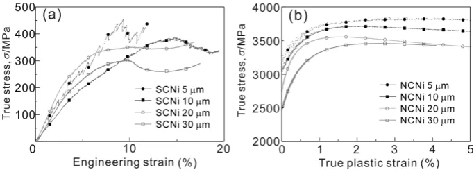
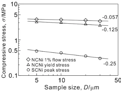
[image:5.595.142.454.67.253.2]cross-section when the cross-sectional area is 1 μm2. In this study, micro-compression specimens with size var-ied from 5 to 30 μm were fabricated from single crystal nick-el with loading axis parallnick-el to the 〈111〉 and the nanocrystal-line nickel26), which hereafter are called SC (single crystal) and NC (nanocrystalline), respectively. SEM images of the pillars before and after the micro-compression tests are shown in Fig. 10. Surface of the deformed SC pillar showed slip traces, which indicates deformations by dislocation move-ments. On the other hand, the NC pillar was deformed by broad shears crossing through the specimen without any cracks. Stress strain curves of each test are shown in Fig. 11. Both of NC and SC specimens are strengthened by reducing the sample size from 30 to 5 μm. Similar to the SC tensile specimen evaluated in section 3, where the 〈111〉 sample had two stages of deformation regime, the linear hardening and the parabolic hardening stages. Work softening was observed in the compression test, which corresponds to the reduction of cross-sectional area by macroscopic shear. The stresses as a function of pillar diameter for the SC and NC pillars are shown in Fig. 12. Slopes of the solid lines are corresponded to scaling exponent of sample size effect m aforementioned in formula 1. The scaling exponent observed for the peak stress of the SC pillar (−0.64) was smaller than the value reported by Dimiduk et. al (−0.25)3). The peak stress includes the ef-fect of work hardening, and thus, the exponent becomes
Fig. 10 SEM images of compression specimens. (a), (b) Nanocrystalline specimens before deformation, (c), (d), single crystal specimens before deforma-tion, (e), (f) nanocrystalline specimens after deformadeforma-tion, and (g), (h) single crystal specimens after deformation.
[image:5.595.126.468.308.432.2]smaller when compared to other reports using yield stress in calculation of the exponents. The NC pillars also showed the size effect even though the exponent is almost 0, the yield stress increased to 600 MPa. Jang and Greer23) reported the sample size effect on 60 nm grain size nickel using nano-sized pillar in compression tests. Their results indicated the strength decreased by decreasing sample size from 3000 nm to 100 nm. They concluded that is a consequence of changing operating deformation mechanisms from dislocation motion to grain boundary sliding in smaller sample size. Assuming from the tension compression asymmetry, the material evalu-ated in this study, nanocrystalline nickel with 8 nm grain size, deformed by grain boundary sliding, and the deformation mechanism did not change in different specimen size. Coop-erative grain boundary sliding is widely accepted as one of the deformation mechanisms via grain boundary, in which mechanism, the deformation involves several grains in forma-tion of micro shear bands along the grain boundaries27,28). Summation of these shear bands formed yields macroscopic strain in the micro-testing. Shear bands formation could initi-ate from flat segment of grain boundaries, and the number of these segments decreased with decreasing sample size. Larg-er samples would have longLarg-er segments of grain boundaries which can deform easily29,30). This is in good agreement with the sample size effect on nanocrystalline nickel evaluated in present work.
5. Conclusions
We have introduced a fabrication method of non-tapered micro-specimens which can be applied in any conventional FIB equipment. Micro-tensile test results using specimens fabricated from single crystal nickel using the non-tapered fabrication method confirmed precision of the method we de-veloped. Micro-compression tests using the non-tapered mi-cro-pillars fabricated from electrodeposited nanocrystalline nickel film demonstrated the nanocrystalline nickel is a prom-ising material for applications as MEMS components. The nickel film prepared by electrodeposition with supercritical
pered micro-specimen fabrication method presented in this work can be applied to process various materials such as thin and small materials, and the results can shed light on the me-chanical properties of small sized materials.
REFERENCES
1) J.R. Greer and J.T.M. De Hosson: Prog. Mater. Sci. 56 (2011) 654.
2) M.D. Uchic, D.M. Dimiduk, J.N. Florando and W.D. Nix: Science 305 (2004) 986.
3) D.M. Dimiduk, M.D. Uchic and T.A. Parthasarathy: Acta Mater. 53 (2005) 4065.
4) H. Zhang, B.E. Schuster, Q. Wei and K.T. Ramesh: Scr. Mater. 54 (2006) 181.
5) K. Boylan, D. Ostrander and U. Erb: Scr. Metall. 25 (1991) 2711.
6) T. Nagoshi, T.F.M. Chang, S. Tatsuo and M. Sone: Microelectron. Eng.
110 (2013) 270.
7) M. Mutoh, T. Nagoshi, T.F. Mark Chang, T. Sato and M. Sone: Micro-electron. Eng. 111 (2013) 118.
8) Y. Kihara, T. Nagoshi, T.F.M. Chang, H. Hosoda, S. Tatsuo and M. Sone: Mater. Lett. 153 (2015) 36.
9) Y. Kihara, T. Nagoshi, T.F.M. Chang, H. Hosoda, T. Sato and M. Sone:
Microelectron. Eng. 141 (2015) 17.
10) M.D. Uchic and D.M. Dimiduk: Mater. Sci. Eng. A 400–401 (2005) 268.
11) R. Honeycombe, ed.: The Deformation of Metals, (Second Edition), (1984).
12) A. Shibata, H. Noda, M. Sone and Y. Higo: Thin Solid Films 518 (2010) 5153.
13) H. Imamura, T. Nagoshi, A. Yoshida, T.F.M. Chang, S. Onaka and M. Sone: Microelectron. Eng. 100 (2012) 25.
14) M.C. Liu, J.C. Huang, K.W. Chen, J.F. Lin, W.D. Li, Y.F. Gao and T.G. Nieh: Scr. Mater. 66 (2012) 817.
15) T.F.M. Chang, M. Sone and H. Uchiyama, (ed.): Advanced Topics on Crystal Growth, (2013).
16) T.F.M. Chang, M. Sone, A. Shibata, C. Ishiyama and Y. Higo: Electro-chim. Acta 55 (2010) 6469.
17) T.F.M. Chang and M. Sone: Surf. Coat. Tech. 205 (2011) 3890.
18) S.T. Chung and W.T. Tsai: J. Electrochem. Soc. 156 (2009) D457.
19) C.Y. Yu, P.W. Kao, C.P. Chang, 53 (2005) 4019.
20) V.V. Bulatov, O. Richmond and M.V. Glazov: Acta Mater. 47 (1999) 3507.
21) A.C. Lund and C.A. Schuh: Acta Mater. 53 (2005) 3193.
22) S. Cheng, J.A. Spencer and W.W. Milligan: Acta Mater. 51 (2003) 4505.
23) D. Jang and J.R. Greer: Scr. Mater. 64 (2011) 77.
24) A. Rinaldi, P. Peralta, C. Friesen and K. Sieradzki: Acta Mater. 56 (2008) 511.
25) R.W. Armstrong: J. Mech. Phys. Solids 9 (1961) 196.
26) T. Nagoshi, M. Mutoh, T.F.M. Chang, T. Sato and M. Sone: Mater. Lett.
117 (2014) 256.
27) M.G. Zelin and A.K. Mukherjee: Acta Metall. Mater. 43 (1995) 2359.
28) V.V. Astanin, A.V. Sisanbaev, A.I. Pshenichnyuk and O.A. Kaibyshev:
Scr. Mater. 36 (1997) 117.
29) H. Muto, Y. Takahashi, T. Futami and M. Sakai: J. Eur. Cera. Soc. 22 (2002) 2437.
[image:6.595.64.270.68.222.2]30) H. Muto and M. Sakai: Acta Mater. 48 (2000) 4161.