Effects of Cu Self-Capping and Ta Capping on Nanometer-Sized Cu Films
Sputter-Deposited on
-Ta
Hisanori Tanimoto
*, Takayuki Sugimori, Shoichiro Kumamoto,
Hazuki Matsui and Hiroshi Mizubayashi
Graduate School of Pure and Applied Sciences, University of Tsukuba, Tsukuba 305-8573, Japan
The Cu(111) texture evolution in Cu films sputter-deposited on 35-nm-Ta barrier layers on Si(100) (Ta/Cu) and in those capped by 5-nm Ta (Ta/Cu/Ta) were studied by X-ray diffraction (XRD). The Cu thicknesses (tCu) ranged from 5 to 500 nm. For Ta/Cu, the intensity of the Cu
111 reflection exhibited a step-like increase fortCubetween 22 and 33 nm, indicating that subsequent deposition of Cu caused the Cu(111)
texture evolution in the already-deposited Cu film (Cu self-capping effect). For Ta/Cu/Ta, the 5-nm Ta capping caused the Cu(111) texture evolution in the already-deposited Cu films fortCubetween 10 and 30 nm (Ta capping effect). These capping effects indicate that the texture
evolution took place at room temperature in nanocrystalline Cu films. The capping effects and the initial growth stage of Cu on-Ta are discussed as they relate to Ta and Cu interfacial and grain boundary energies in the nanocrystalline structures.
[doi:10.2320/matertrans.M2010286]
(Received August 30, 2010; Accepted October 15, 2010; Published December 1, 2010)
Keywords: copper, tantalum, thin film, capping effect, interface energy, grain boundary, nanocrystalline structurte
1. Introduction
Understanding the properties and structures of Cu thin films deposited on barrier films made from materials such as Ta and TiN is important for developing high-performance microelectronic devices. The Cu-Ta system is a typical immiscible example; therefore, its microstructure is also of great interest from a scientific perspective. Many studies have focused on the resistivity and electromigration,1–3)
mechan-ical properties,4–6) and microstructures7–10) of Cu films
formed on Ta. Interconnections between films with sizes of less than a few tens of nanometers, such as nanometer-thick Cu films on nanometer-thick Ta barrier layers, require control of their microstructures for use as strong heterogeneous film-barrier systems. The growth behavior is very important for the preparation of nanometer-thick metallic films, and it depends on the interfacial state between the film and its underlayer. There are three well-known modes of growth for metallic thin films prepared by deposition: a layer-by-layer growth (Frank-van der Merwe (FM) mode), a three-dimen-sional-island growth (Volmer-Weber (VM) mode), and a transitional mode from the initial layer-by-layer growth to the three-dimensional-island growth with increasing deposition thickness (Stranski-Krastanov (SK) mode). For Cu growth on a clean Ta surface, the formation of approximately one conformal Cu monolayer with high thermal stability has been reported from experiments7,11,12) and calculations.10,13,14)
These reports suggest that Cu grows in the SK growth mode on Ta. The crystallographic texture and elastic property of Cu films sputter-deposited on Ta are expected to change with the Cu thickness in the nanometer-thick range.
The Cu thickness dependence of the crystallographic texture and elastic property of Cu films sputter-deposited on 35-nm-thick Ta barrier films (Ta/Cu) and 5-nm-thick Ta capped films (Ta/Cu/Ta) were studied for Cu thicknesses
between 10 and 1000 nm in our previous investigations.4,15)
Reed-shaped Si substrates were used to measure the elastic property of the Cu thin films using the complex reed vibration method.16,17) After intensive chemical etching, the Si sub-strates exhibited undulated surfaces, and the deposited 35-nm-thick Ta barrier films were composed of equilibrium -Ta and nonequilibrium-Ta.4)For Cu film thicknesses (tCu)
below80nm, both the crystallographic texture and elastic property exhibited considerable changes with the Cu film thickness, as well as after Ta capping. For example, the in-plane Young’s modulus of the Cu films decreased with
tCu for Ta/Cu and was enhanced after 5-nm Ta-capping for
Ta/Cu/Ta. The Cu (111) plane distance (dCu111) normal to
the film surface decreased withtCu for Ta/Cu (0:3% from
the bulk value attCuof 20 nm), and such a decrease indCu111
almost disappeared after 5-nm Ta capping for Ta/Cu/Ta. Because the Cu thin films were not only prepared on the barrier film but also capped or surrounded by the barrier layers in the microelectronic devices, it is important to understand these phenomena from the previous work.
During Ta deposition on Si, the nonequilibrium -Ta phase is preferentially formed by sputter-deposition on Si or SiO2.12,18–22) In our previous work, the Ta barrier layers
deposited on Si reed substrates with undulated surfaces consisted of an equilibrium-Ta phase and-Ta phase.4)In
contrast, the Ta barrier layers deposited on Si reed substrates with a mirror surface consisted solely of the -Ta phase.15)
On the other hand, on-Ta, but not on-Ta, the formation of a superstructured Cu layer has been reported in a recent computer simulation study of the deposition of an fcc Cu film on Ta.10) These results indicate that further study of the
microstructure of Cu films deposited on-Ta films formed on Si substrates with a mirror surface is technologically and scientifically relevant. In the present study, we used Si wafers with a mirror surface as substrates and investigated the Cu thickness dependence of the microstructure of nanometer-thick Cu films deposited on-Ta and of those capped with 5-*Corresponding author, E-mail: [email protected]
nm thick Ta by X-ray diffraction (XRD). FortCu<100nm,
all Cu films exhibited a preferred (111) texture in which the (111) planes of most crystallites were parallel to the flat surface of the sample. For Ta/Cu, the Cu-thickness depend-ence of the intensity of the 111 reflection exhibited a step-like increase attCubetween 22 and 33 nm, indicating spontaneous
improvement of the preferred (111) texture in the already-deposited Cu films by subsequent deposition of Cu (Cu self-capping effect). For Ta/Cu/Ta, the spontaneous improve-ment of the preferred (111) texture in the already-deposited Cu films by 5-nm-thick Ta capping occurred attCu between
10 and 30 nm (Ta capping effect).
2. Experimental Procedure
Si (100) wafers (¼2in., 0.4-mm thick) that were mirror-polished on one side, were cut into rectangular pieces having a length and width of 1.3 cm and 2 cm, respectively. These substrates were rinsed with ethanol in an ultrasonic bath, and organic contamination was chemically removed using a mixed solution of H2SO4and H2O2. Finally, the surfaces of
the Si substrates were terminated by hydrogen using a dilute HF solution.
Deposition of Ta and Cu was carried out using DC magnetron sputtering equipment (ULVAC MPS-2000) under 1:3101Pa Ar at ambient temperatures. The nominal
purity of Ar was 99.9999%. The distance between the substrate and the target was 200 mm. We applied 50 W each of rf and dc power to the coil for helicon wave generation and to the target (Ta (99.95%) or Cu (99.999%), ¼2in.), respectively. The film growth rates of Ta and Cu were approximately 2 and 5 nm/min, respectively. The thicknesses of the deposited Ta and Cu were determined based on the weight change of an Al foil located near the substrate. For Ta/Cu, a 35-nm-thick Ta barrier layer was deposited on the Si substrate, and a Cu film with the desired thickness was subsequently deposited on the Ta barrier layer without breaking the Ar atmosphere. For Ta/Cu/Ta, a 5-nm-thick Ta capping layer was further deposited on the Cu film without breaking the Ar atmosphere. To examine the morphology of the Ta barrier layer, a 35-nm-thick Ta barrier layer was deposited on the Si substrate (Ta barrier alone). A single Cu (111) crystal with a diameter of 10 mm and thickness of 0.5 mm was used as a model sample with a fully preferred oriented state. Cu pellets were prepared by compacting Cu powder (10-mmgrains) for reference samples of polycrystal-line bulk Cu with fully random textures. The porosity of the Cu pellets was determined from their weight and dimensions. XRD measurements in the2-scan mode were performed with Cu-Kradiation (40 keV, 30 mA, Rigaku RINT 2100). The scattering vector was normal to the film. The axes of2 and were adjusted according to the maximum Cu 111 reflection intensity prior to the2-scan, and a 1divergence
slit was used. The 111 reflection from the Cu single crystal was used as the instrumental line broadening for an estimation of the mean grain size. Reflections from Si powders placed on the film surface were used as references for the2scale. XRD measurements in the!scan mode (2 scan withat the Bragg position of the Cu 111 reflection) were also conducted for several samples.
3. Results and Discussion
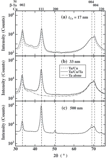
Figures 1(a)–(c) show example XRD spectra for the Ta/Cu and Ta/Cu/Ta samples deposited on mirror Si substrates withtCu of 17, 33, and 500 nm, respectively. The
spectrum for the sample composed of the Ta barrier alone is also shown in Fig. 1(b). There were no reflections of-Ta; only the 002 and 004 reflections of -Ta were observed, indicating that the 35-nm-thick Ta barrier layer consisted of -Ta with a highly preferred (001) texture, in which the (001) planes of most crystallites were parallel to the flat surface of the film. In the XRD spectra for Ta in Ta/Cu and Ta/Cu/Ta, only the 002 and 004 reflections of-Ta were observed for all Ta/Cu and Ta/Cu/Ta samples with tCu between 5 and
500 nm. This indicates that the 35-nm-thick Ta barrier layers remained as-Ta with the highly preferred (001) texture after Cu film deposition and that the 5-nm Ta capping layers also had the same texture. Figures 1(a) and (b) show that the base of the -Ta 002 reflection for Ta/Cu/Ta withtCu of 17 or
33 nm was broader than that for Ta/Cu because of the overlap of the additional reflection from the 5-nm Ta capping layer. In contrast, Fig. 1(c) shows that the base of the -Ta 002 reflection due to the 5-nm-thick Ta capping layer was smeared by increased background scattering from the 500-nm-thick Cu film.
30 40 50 60 70
102
104
106
2θ ( ° )
Intensity (Counts)
500 nm (c)
102
104
106
Intensity (Counts)
33 nm (b) Cu
Ta/Cu Ta/Cu/Ta Ta alone
102
104
106
Intensity (Counts)
β-Ta
111
004 220
tCu = 17 nm
(a)
Si 004
002
200
Fig. 1 X-ray diffraction patterns for Ta/Cu (dashed lines) and Ta/Cu/Ta (solid lines) for Cu film thicknesses of (a) 17 nm, (b) 33 nm, and (c) 500 nm. In (b), the pattern for the Ta barrier alone (35 nm) is also shown (dotted/dashed line). The broad peak at 2¼69:2 is the Si 400
[image:2.595.318.534.74.394.2]The XRD spectra for Cu in Ta/Cu withtCuof 17 and 33 nm
(Figs. 1(a) and (b)) show that only the 111 reflection of fcc Cu was seen in the2range shown here, and only the Cu 222 reflection was seen in the2range of 76–100 (not shown
here). For Ta/Cu withtCuof 500 nm, minor Cu 200 and 220
reflections were observed in addition to the major Cu 111 reflection (Fig. 1(c)). The Cu 200 and 220 reflections were detected fortCu>200nm. AttCuof 17 nm, the profile of the
Cu 111 reflection in Ta/Cu/Ta was almost the same as that in Ta/Cu (Fig. 1(a)). However, the peak intensity of the Cu 111 reflection was higher in Ta/Cu/Ta than in Ta/Cu. The latter feature suggests that the 5-nm-thick Ta capping caused some modification of the crystallographic texture in the already-deposited Cu film. In contrast, attCu of 33 nm, both
the profile and intensity of the Cu 111 reflection showed good agreement between Ta/Cu and Ta/Cu/Ta (Fig. 1(b)), i.e., there was no modification of the crystallographic texture in the already-deposited Cu film by the 5-nm-thick Ta capping layer. AttCu of 500 nm, the major Cu 111 reflection and the
minor Cu 200 and 220 reflections in Ta/Cu/Ta were in good agreement with those in Ta/Cu (Fig. 1(c)).
The XRD results above indicate that the present Cu films sputter-deposited on the -Ta barrier layer had the highly preferred (111) texture, in which the (111) planes of most crystallites were parallel to the flat surface of the specimen. Furthermore, the degree of alignment in the preferred (111) texture of the already-deposited Cu films withtCubetween 10
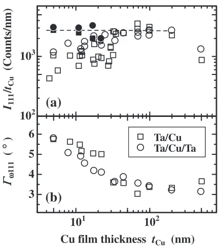
and 30 nm was modified by capping with the 5-nm-thick Ta layer. Figure 2 shows the dependence of the integral intensity of the Cu 111 reflection (I111) for Ta/Cu and Ta/Cu/Ta on
the value oftCu. From the mass absorption of the X-ray, the
dependence ofI111ontCu can be expressed by the following
equation:23)
I¼I0expð2tCu=sin111Þ: ð1Þ
whereI0 is the intensity of the incident X-ray;, the mass
absorption coefficient of Cu-Kradiation for Cu; and111,
the Bragg angle for the Cu 111 reflection. The intensity of the XRD reflection depends on the dimensions as well as on the crystallinity of a sample. ThetCudependence ofI111for the
(111) single crystalline state was estimated from the I111
measured for the Cu (111) single crystal sample (¼10mm, 0.5-mm thick) under the same measurement conditions, based on eq. (1). Figure 2 shows the result as a solid line as a guide for the fully preferred (111) texture state. The dotted/ dashed line shown in Fig. 2 denotes the dependence ofI111on tCu for the fully random-oriented polycrystalline state, in
which I111 for Cu pellets was measured under the same
conditions, and thetCu dependence was estimated based on
eq. (1) as well as the influence of porosity on intensity. For Ta/Cu samples shown in Fig. 2, all of theI111data are
between the values expected for the fully (111) textured and fully random states. The slope of thetCudependence ofI111in
Ta/Cu at tCu between 33 and 100 nm agreed well with that
expected from eq. (1). The I111 value observed at tCu of
500 nm exhibited a downward deviation from the line extrapolating the tCu dependence of I111 between 33 and
100 nm in Fig. 2. This was associated with the appearance and increase in the Cu 200 and 220 reflections at tCu>
200nm, as mentioned previously. FortCu>22nm, the slope
of the tCu dependence of I111 for Ta/Cu exhibits good
agreement with that for tCu between 33 and 100 nm.
However, the I111 values for tCu<22nm were about
one-half of those expected from the tCu dependence of I111
between 33 and 100 nm. Figure 3(a) shows I111 normalized
bytCu (I111=tCu), and a step-like decrease attCu between 22
and 33 nm is clearly seen for Ta/Cu. The data for Ta/Cu/Ta exhibit a gradual increase inI111=tCu attCu between 10 and
30 nm because of the 5-nm-thick Ta capping.
Figure 4 shows the XRD spectra for the Cu 111 reflection in the!scan mode. The integrated intensity was normalized
10
110
210
410
510
6I
111(Counts)
fully (111) textured
fully random
Cu film thickness
t
Cu(nm)
Ta/Cu Ta/Cu/Ta
Fig. 2 tCudependencies forI111. The solid line and dotted/dashed lines
show thetCudependence expected for the Cu (111) single crystalline state
and the fully random-oriented polycrystalline state, respectively. The dashed line shows the results of fitting eq. (1) using the observed data at tCubetween 33 and 100 nm.
10
110
23
4
5
6
Γ
ω111
(
°
)
Cu film thickness
t
Cu(nm)
(b)
Ta/Cu Ta/Cu/Ta
10
210
3I
111/
t
Cu(Counts/nm)
(a)
Fig. 3 (a)tCudependencies ofI111normalized bytCu(open symbols) and
those revised by accounting for differences in the preferred texture (filled symbols, see text for details). (b)tCudependence of the full width at half
[image:3.595.318.534.71.257.2] [image:3.595.319.534.340.583.2]for all peaks. A broader peak in the!scan mode indicates weaker alignment in the preferred (111) orientation of the crystallites. AttCu of 5 nm, the peak profiles for Ta/Cu and
Ta/Cu/Ta were broad and nearly identical. AttCu of 17 nm,
the peak profiles for both Ta/Cu and Ta/Cu/Ta were sharper than their counterparts attCuof 5 nm, and the peak of
Ta/Cu/Ta with the 5-nm-thick Ta capping was sharper than that of Ta/Cu. At tCu of 33 nm, the peak profiles for both
Ta/Cu and Ta/Cu/Ta were sharper than their counterparts attCuof 17 nm, but further sharpening due to the 5-nm-thick
Ta capping was not observed. To evaluate the degree of alignment in the preferred (111) texture, the full width at half maximum (!111) was determined by assuming that
the peak profile was approximated by a Gaussian function. The tCu dependence of !111 is shown in Fig. 3(b). As tCu
increased, !111 for Ta/Cu exhibited a gradual decline for tCu <22nm, a step-like decrease at tCu between 22 and
33 nm, and then saturation at 3 for larger t
Cu. After the
5-nm-thick Ta capping, !111 for Ta/Cu/Ta exhibited a
gradual decrease to3with increasingt
Cu. In other words,
peak sharpening in the!scan mode occurred attCubetween
10 and 30 nm after the 5-nm-thick Ta capping. Apparently, the lack of Ta capping effects on !111 attCu>30nm was
associated with saturation of the!111sharpening at3for
both Ta/Cu and Ta/Cu/Ta.
Because a divergence slit of 1 was used in the present
XRD measurements, the crystallites involved in the 111 reflection peak in the2-scan mode were those whoseh111i directions were within 0.5 from the scattering vector. That
is, the area fraction within 0.5from the top of the peak in the ! scan peak (R) is the fractional ratio of the crystallites contributing to ICu111 in the present 2- scan mode. In
Fig. 3(a), the filled symbols fortCu<33nm are theI111=tCu
values calibrated usingRat a giventCuand normalized byR33
at tCu of 33 nm as a reference, ðI111=tCuÞ=ðR=R33Þ. The
ðI111=tCuÞ=ðR=R33Þ data for both Ta/Cu and Ta/Cu/Ta
exhibited good agreement with the mean value for ðI111=tCuÞ=ðR=R33Þ in Ta/Cu between 33 and 100 nm. The
reducedI111=tCuin Ta/Cu attCu<33nm was associated with
weaker alignment in the preferred (111) texture. In other words, alignment of the preferred (111) texture in the already-deposited Cu film spontaneously improved as a result of capping with the Cu overlayers (Cu self-capping effect) at tCu between 22 and 33 nm. The data for Ta/Cu/Ta in
Fig. 3(a) indicate that the spontaneous improvement of the preferred (111) texture in the already-deposited Cu film by the 5-nm-thick Ta capping (Ta capping effect) also occurred attCubetween 10 and 30 nm.
The spontaneous improvement in the alignment of the preferred (111) texture in the already-deposited Cu films was attributed to rotation of the crystallites. In this case, the mean rotated angle was expected to be a few degrees based on the !111data shown in Fig. 3(b). Spontaneous grain rotation of
constituent nanocrystallites without grain growth has been reported for nanocrystalline (n-) Au during plastic creep deformation under applied stress>30MPa at room temper-ature.24)A close similarity in the mechanisms of plastic creep deformation was reported betweenn-Au andn-Cu.25)These phenomena also suggest that for the present Cu films in Ta/Cu and Ta/Cu/Ta, both the Cu self-capping and the Ta capping effects were associated with spontaneous grain rotations in the already-deposited Cu films. For the Cu self-capping, the driving force for spontaneous rotation was attributed to the self-adjustment of the crystallographic directions in the already-deposited film induced by lateral growth of the crystallites in the capping layer. When a new crystallite formed on the polycrystalline film, nucleation at the triple junctions most likely occurred. Theh111i orienta-tions of the new crystallite formed at the triple juncorienta-tions, as well as the crystallites beneath it, adjusted in one direction to reduce the mismatch between their interfaces. For the Ta capping effect, the strong interaction between Cu and Ta was attributed to the driving force (see below). There were no Ta capping effects at tCu<10nm; thus,tCu of 10nm
corre-sponded to the transitional thickness for initially formed islands that transitioned to a continuous film. Below tCu of
10nm, the interfacial interaction between the Cu films and the Ta barrier was larger than that between the Cu films and the Ta capping. The gradual Ta capping effect observed for Ta/Cu/Ta at tCu between 10 and 30 nm indicates that the
-Ta barrier effects on the microstructure of deposited Cu crystallites ceased attCu of 30 nm. The effects of the mixed
Ta barrier composed of-Ta and-Ta on the microstructure of deposited Cu crystallites continued up to tCu of 80 nm,
as previously mentioned.4,15)
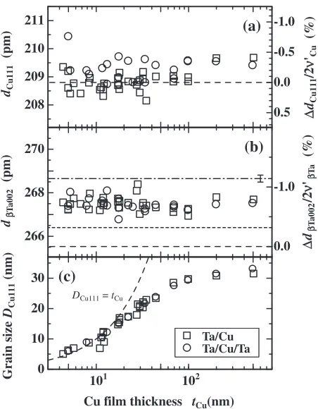
Figure 5(a) shows the tCu dependence of the interlayer
distance for Cu (111) (dCu111) normal to the film surface,
as determined from their respective XRD peak positions. Successive alternations in the in-plane stress from
compres-tCu = 5 nm
17 nm
-5
0
5
33 nm
θ
-
θCu111
(
°
)
Normalized Intensity
(a)
(b)
(c)
Fig. 4 Profiles of X-ray diffraction peaks in the!-scan mode for the Cu 111 reflection of Ta/Cu (dashed lines) and Ta/Cu/Ta (solid lines) attCuof
[image:4.595.82.257.69.368.2]sive to tensile and back to compressive with increasing tCu
were reported for the three-dimensional island growth mode.26,27) Quantitatively, d
Cu111 in Ta/Cu at tCu of 5 nm
was0:2% larger than the bulk Cu value, indicating that the in-plane compressive strain (or stress) in a 5-nm-thick Cu film on a 35-nm-thick Ta barrier layer was 0:25% (or 0.5 GPa) (see the right-hand side vertical axis in Fig. 5(a)), assuming a mean Poisson ratio of 0.343 and a mean Young’s modulus of 130 GPa28)along the direction of the film. Ast
Cu
increased above 5 nm,dCu111in Ta/Cu decreased to a slightly
smaller value than the bulk Cu value, exhibited a local minimum attCuof10nm, and then increased slightly above
the bulk Cu value attCuabove30nm. ThetCuvalues of the
crossover points for these successive changes exhibited good agreement with those reported (i.e., the first crossover from compressive to tensile states attCubetween 1 and 20 nm, and
again to the compressive state at tCu between 4 and 40 nm,
respectively).26) The first crossover from compressive to tensile states was observed when the initially formed islands transitioned to a continuous film. That is, when the reduction in the total surface and interface energies by contacting neighboring islands was larger than the increase in the strain energy of the resultant continuous film, the isolated islands
coalesced and formed a continuous film (the zipping effect).29)A tensile stress of1GPa in the continuous film
was estimated from model calculations for the zipping effect.30)In Fig. 5(a), the compressive stress of0:5GPa for
Cu attCuof 5 nm became nearly zero or slightly tensile fortCu
between 10 and 30 nm, indicating that the island-like film transitioned to a continuous film at tCu of 10nm in the
present Ta/Cu films.dCu111exhibited a local maximum attCu
of 30nm that was slightly larger than the bulk value. Because the spontaneous improvement of the preferred (111) texture caused by the Cu self-capping was seen for tCu
between 22 and 33 nm (Fig. 3(a)), the in-plane compressive stress may have been induced by the Cu self-capping effect. AttCu above 30 nm,dCu111first exhibited a slight decline to
the bulk value attCuof100nm and then increased slightly
attCu above 200 nm. As mentioned above, the 200 and 220
reflections appeared attCu>200nm. These changes in both
dCu111and the XRD spectra suggest that the growth mode of
the Cu films further changed attCubetween 100 and 200 nm.
For Ta/Cu/Ta,dCu111was almost constant fortCufrom 10 to
500 nm and larger by0:3% than that of the bulk value. The values ofdCu111in Ta/Cu/Ta were slightly larger than those
in Ta/Cu at tCu between 10 and 30 nm, at which the
spontaneous improvement of the preferred (111) texture by the 5-nm-thick Ta capping was observed (Fig. 3(a)). The spontaneous improvement of the preferred (111) texture may have been responsible for the slightly largerdCu111values in
Ta/Cu/Ta at tCu between 10 and 30 nm. In contrast, the
increase indCu111by the 5-nm-thick Ta capping was observed
up totCuof80nm in our previous studies4,15)and indicates
that the effects of the mixed Ta barrier composed of -Ta and-Ta on the deposited Cu microstructures continued up to
tCu of 80 nm, as previously mentioned.
Figure 5(b) shows the tCu dependence of the interlayer
distance for-Ta (002) (dTa002) normal to the film surface,
as determined from their respective XRD peak positions. The dotted/dashed line in Fig. 5(a) denotes a dTa002 of
268.65 pm in the 35-nm-thick Ta barrier alone. For the bulk value, adTa002of 266.4 pm was reported for a 30-mm-thick
-Ta film deposited on an AISI4340 steel substrate,21)
whereas a value of 265.32 pm was reported for a 20-mm -Ta single crystal.31)The largerdTa002as compared to the
bulk values indicates that the present 35-nm-thick-Ta films sputter-deposited on Si(100) were in a compressed state along the surface of the film. The in-plane compressive strain (or stress) estimated for the 35-nm-thick-Ta barrier alone ranged from 0.7 to 1.2% (or 1.3–2 GPa) using the bulk values of dTa002 mentioned above, a biaxial modulus of 175 GPa
for the -Ta film along the (001) plane,32) and a Poisson
ratio of 0.3. In Cr films (but not in -Ta films) on Si, the compressive stress was reported to have increased with decreasing film thickness (tf).33) Application of the
film-thickness dependence of the internal stress reported in Cr films to the present case gave a compressive stress of 2.0 GPa at a thickness of 35 nm, exhibiting good agreement with the estimated compressive stress in the 35-nm-thick Ta barrier layer. On the other hand, the dTa002 values of both
Ta/Cu and Ta/Cu/Ta decreased as compared to that of the Ta barrier alone (Fig. 5(b)). The in-plane compressive strain (or stress) of the barrier decreased to 0.4–0.7% (or 0.7–
208 209 210
211 -1.0
-0.5
0.0
0.5
dCu111
(pm)
(a)
∆
dCu111
/2
ν
'Cu
(%)
101 102
0 10 20 30
Cu film thickness tCu(nm)
Grain size
DCu111
(nm)
(c)
Ta/Cu Ta/Cu/Ta
DCu111 = tCu
266 268 270
-1.0
0.0
dβ
Ta
0
0
2
(pm)
(b)
∆
dβ
Ta
0
0
2
/2
ν
'βTa
(%)
Fig. 5 (a) Dependence of the Cu (111) interlayer distance (dCu111) ontCu.
The dashed line indicates the dCu111 value reported for bulk Cu. (b)
Dependence of the-Ta (002) interlayer distance (dTa002) ontCu. The
dotted/dashed line indicates the mean value for three samples of the 35-nm-thick Ta barrier alone. The dashed lines indicate thedTa002values
reported for a 30-mm-thick -Ta film deposited on an AISI4340 steel substrate (266.4 pm)21) and for a 20-mm-thick -Ta single crystal
(265.32 pm).31) The ordinate on the right-hand side shows the scale
converted to the in-plane strain, where thedTa002reported for the-Ta
single crystal is considered as the bulk value. (c) Dependence of the mean grain size of the Cu film (DCu111) ontCu. The dashed line indicates the
[image:5.595.56.282.70.360.2]1.3 GPa) after deposition of a Cu film, suggesting that there was a strong elastic interaction at the interface between the Cu film and the Ta barrier. The fcc Cu (111) plane has been reportedly grown heteroepitaxially on the-Ta (002) plane with a lattice mismatch of 7.6%,34)and the interface between
fcc Cu and -Ta exhibited high thermal stability.18) As
previously mentioned for the SK growth mode of the Cu films on-Ta, the formation of one conformal monolayer of Cu can decrease the in-plane compressive strain (or stress) in the Ta barrier and weaken the Cu-thickness dependence of thedTa002values of both Ta/Cu and Ta/Cu/Ta, as shown
in Fig. 5(b). A small local minimum observed at tCu
100nm for the Cu-thickness dependence of thedTa002values
may have been associated with a change in the growth mode of the Cu films (i.e., the transition from the (111) textured structure to the randomly textured structure began at tCu
between 100 and 200 nm).
Figure 5(c) shows the Cu-thickness dependence of the mean grain size normal to the film surface (DCu111), estimated
from the width of the Cu 111 reflection using the Scherrer equation. The instrumental line broadening was corrected from the 111 reflection observed for the Cu single crystal sample. The nearly identical Cu-thickness dependence of
DCu111 between Ta/Cu and Ta/Cu/Ta supports the
conclu-sion that the 5-nm-thick Ta capping did not cause grain growth but may have improved the alignment in the preferred (111) texture in Cu films by spontaneous rotational motion of the crystallites. As shown in Fig. 5(c), DCu111 was nearly
identical to the Cu film thickness for tCu below 10nm,
at which island-like Cu film growth following coverage with one conformal monolayer was expected, as mentioned previously. FortCu>10nm, the increase inDCu111exhibited
saturation at30nm fortCu>100nm (Fig. 5(c)). At thistCu,
continuous Cu film growth in the SK mode and cessation of the effect of-Ta barrier on the Cu film growth were likely. Then, the saturation of DCu111 at30nm for tCu>100nm
(Fig. 5(c)) suggests that the 30nm crystallites were thermally stable in the present Cu films. The mean grain size in nanocrystalline Cu with the preferred (111) texture prepared by various methods have been commonly reported at 25–30 nm.25,35) That is, constituent nanocrystallites with grain sizes of 25–30 nm were in a quasi-stable state in nanocrystalline Cu with the preferred (111) texture. Very similar results for the grain size stabilization in nanostruc-tured fcc metals with the preferred (111) texture have been found in n-Au.24,36) In contrast, in the nanocrystalline Cu
films deposited on the mixed Ta barrier composed of-Ta and-Ta, the mean grain size increased beyond 30 nm and exhibited a poorly preferred (111) texture.4,15) This again
suggests that the effects of the mixed Ta barrier composed of-Ta and-Ta on the deposited Cu crystallites continued up totCu of 80 nm.
4. Conclusion
Cu films were sputter-deposited on 35-nm-thick -Ta barrier films, and changes in their texture as a function of Cu thickness and by 5-nm-thick Ta capping were investigated. For the Cu-thickness (tCu)<100nm, all Cu films exhibited
a highly preferred (111) texture in which the (111) planes
of most crystallites were parallel to the flat surface of the sample. For Cu films without Ta capping (Ta/Cu), the Cu-thickness dependence of the integral intensity of the 111 reflection exhibited a step-like increase attCubetween 22 and
33 nm, indicating spontaneous improvement of the preferred (111) texture in the already-deposited Cu films by subsequent deposition of Cu (Cu self-capping effect). For Cu films with the 5-nm-thick Ta capping (Ta/Cu/Ta), the spontaneous improvement of the preferred (111) texture in the already-deposited Cu films by 5-nm-thick Ta capping occurred attCu
between 10 and 30 nm (Ta capping effect). Both these effects were associated with spontaneous rotational motion of the Cu crystallites. For creep deformations (but not for film deposition), such spontaneous rotational motion of the crystallites has been reported in nanocrystalline Cu and nanocrystalline Au. In the present study, reduction in the total surface and interface energies caused self-adjustment of the crystallographic directions in the already-deposited Cu films. The mean grain size in the Cu films with the preferred (111) texture deposited on-Ta barrier films exhibited saturation at 30nm, whereas that in the Cu films with a poorly preferred (111) texture deposited on the mixed Ta barrier composed of -Ta and -Ta increased beyond 30 nm, as reported in previous works. These observations indicate that grain sizes of 25–30 nm were in a quasi-stable state in nanocrystalline Cu with the preferred (111) texture.
The present experimental results indicate the following model for the microstructural evolution of nanometer Cu films deposited on -Ta barrier. At the initial stage of Cu deposition, one conformal Cu monolayer was formed on the -Ta barrier, and it decreased the in-plane compressive strain (or stress) in the -Ta barrier on the Si(100) substrate. Then, isolated island growth of Cu occurred with increasing deposited Cu thickness up to10nm, where the degree of the preferred (111) texture in the Cu films remained poor, and neither Cu self-capping effects nor Ta capping effects were expected. Above a Cu thickness of 10nm, the isolated islands coalesced and formed a continuous film, where the degree of the preferred (111) texture in the Cu films improved, and both Cu self-capping effects and Ta capping effects were expected. After saturation of the enhanced preferred (111) texture in the Cu films for a Cu thickness of 30nm, both Cu self-capping effects and Ta capping effects disappeared. The present results reemphasize the technological scientific importance of a controlled interface and grain boundaries for nanometer-sized devices.
Acknowledgement
This study was financially supported by a Grant-in-Aid for Scientific Research from the Japan Society for the Promotion of Science.
REFERENCES
1) H. Mizubayashi, K. Goto, T. Ebisawa and H. Tanimoto: Mater. Sci. Eng. A442(2006) 342.
2) V. Timoshevskii, Y. Ke, H. Guo and D. Gall: J. Appl. Phys.103(2008) 113705.
(2006) 336.
5) A. Hashibon, C. Elsa¨sser, Y. Mishin and P. Gumbsch: Phys. Rev. B76
(2007) 245434.
6) P. A. Gruber, J. Bo¨hm, F. Onuseit, A. Wanner, R. Spolenak and E. Arzt: Acta Mater.56(2008) 2318.
7) L. Chen, N. Magtoto, B. Ekstrom and J. Kelber: Thin Solid Films376
(2000) 115.
8) X. Zhao, M. Leavy, N. P. Magtoto and J. A. Kelber: Appl. Phys. Lett.
79(2001) 3479.
9) K. Abe, Y. Harada, M. Yoshimaru and H. Onoda: J. Vac. Sci. Technol. B22(2004) 721.
10) I. Lazic, P. Klaver and B. Thijsse: Phys. Rev. B81(2010) 045410. 11) W. K. Kuhn, R. A. Campbell and D. W. Goodman: J. Phys. Chem.97
(1993) 446.
12) F. Fillot, Zs. To¨kei and G. P. Beyer: Surf. Sci.601(2007) 986. 13) T. P. C. Klaver and B. J. Thijsse: J. Computer-Aided Mater. Design10
(2003) 61.
14) A. Hashibon, A. Y. Lozovoi, Y. Mishin, C. Elsa¨sser and P. Gumbsch: Phys. Rev. B77(2008) 094131.
15) H. Tanimoto, K. Fujiwara and H. Mizubayashi: Sci. Technol. Adv. Mater.6(2005) 620.
16) B. S. Berry and A. C. Pritchet: J. Physique (Paris)42(1981) C5-1111. 17) H. Mizubayashi, Y. Yoshihara and S. Okuda: Phys. Status Solidi (a)
129(1992) 475.
18) K.-W. Kwon, H.-J. Lee and R. Sinclair: Appl. Phys. Lett.75(1999) 935.
19) H. Donohue, J. C. Yeoh, K. Giles and K. Buchanan: Micro. Eng.64
(2002) 299.
20) S. Kohli, P. R. McCurdy, C. D. Rithner, P. K. Dorhout, A. M. Dummer, F. Brizuela and C. S. Menoni: Thin Solid Films404(2004) 469.
21) A. Jiang, T. A. Tysona, L. Axe, L. Gladczuk, M. Sosnowski and P. Cote: Thin Solid Films479(2005) 166.
22) J. W. Bae, J.-W. Lim, K. Mimura and M. Isshiki: Thin Solid Films515
(2007) 4768.
23) B. D. Cullity: Elements of X-ray Diffraction, 2nd ed., (Addison-Wesley, Massachusetts, 1978) pp. 4–10.
24) N. Yagi, A. Rikukawa, H. Mizubayashi and H. Tanimoto: Phys. Rev. B
74(2006) 144105.
25) N. Yagi: Dr. Thesis, Institute of Materials Science, University of Tsukuba (2007).
26) G. C. A. M. Janssen: Thin Solid Films515(2007) 6654. 27) F. Spaepen: Acta Mater.48(2000) 31.
28) Smithells Metals Reference Book, 7th ed., ed. by E. A. Brandes and G. B. Brook, (Butterworth-Heinemann, Oxford, 1992) Chap. 15, p. 15-2.
29) J. A. Floro, S. J. Hearne, J. A. Hunter, P. Kotula, E. Chason, S. C. Seel and C. V. Thompson: J. Appl. Phys.89(2001) 4886.
30) W. D. Nix and B. M. Clemens: J. Mater. Res.14(1999) 3467. 31) A. Arakcheeva, G. Chapuisa and V. Grinevitch: Acta Cryst. B 57
(2002) 1.
32) R. Knepper and S. P. Baker: Appl. Phys. Lett.90(2007) 181908. 33) G. C. A. M. Janssen and J.-D. Kamminga: Appl. Phys. Lett.85(2004)
3086.
34) K.-W. Kwon, C. Ryu, R. Sinclair and S. S. Wong: Appl. Phys. Lett.71
(1997) 3069.
35) B. Cai, Q. P. Kong, L. Lu and K. Lu: Mater. Sci. Eng. A286(2000) 188.