A Thesis Submitted for the Degree of PhD at the University of Warwick
http://go.warwick.ac.uk/wrap/49665
This thesis is made available online and is protected by original copyright. Please scroll down to view the document itself.
JHG 05/2011
Library Declaration and Deposit Agreement
1. STUDENT DETAILS
Please complete the following:
Full name: ………. University ID number: ………
2. THESIS DEPOSIT
2.1 I understand that under my registration at the University, I am required to deposit my thesis with the University in BOTH hard copy and in digital format. The digital version should normally be saved as a single pdf file.
2.2 The hard copy will be housed in the University Library. The digital version will be deposited in the University’s Institutional Repository (WRAP). Unless otherwise indicated (see 2.3 below) this will be made openly accessible on the Internet and will be supplied to the British Library to be made available online via its Electronic Theses Online Service (EThOS) service.
[At present, theses submitted for a Master’s degree by Research (MA, MSc, LLM, MS or MMedSci) are not being deposited in WRAP and not being made available via EthOS. This may change in future.] 2.3 In exceptional circumstances, the Chair of the Board of Graduate Studies may grant permission for an embargo to be placed on public access to the hard copy thesis for a limited period. It is also possible to apply separately for an embargo on the digital version. (Further information is available in the Guide to Examinations for Higher Degrees by Research.)
2.4 If you are depositing a thesis for a Master’s degree by Research, please complete section (a) below. For all other research degrees, please complete both sections (a) and (b) below:
(a) Hard Copy
I hereby deposit a hard copy of my thesis in the University Library to be made publicly available to readers (please delete as appropriate) EITHER immediately OR after an embargo period of ………... months/years as agreed by the Chair of the Board of Graduate Studies. I agree that my thesis may be photocopied. YES / NO (Please delete as appropriate) (b) Digital Copy
I hereby deposit a digital copy of my thesis to be held in WRAP and made available via EThOS. Please choose one of the following options:
EITHER My thesis can be made publicly available online. YES / NO(Please delete as appropriate) OR My thesis can be made publicly available only after…..[date] (Please give date)
YES / NO(Please delete as appropriate) OR My full thesis cannot be made publicly available online but I am submitting a separately identified additional, abridged version that can be made available online.
JHG 05/2011
Rights granted to the University of Warwick and the British Library and the user of the thesis through this agreement are non-exclusive. I retain all rights in the thesis in its present version or future versions. I agree that the institutional repository administrators and the British Library or their agents may, without changing content, digitise and migrate the thesis to any medium or format for the purpose of future preservation and accessibility.
4. DECLARATIONS
(a) I DECLARE THAT:
I am the author and owner of the copyright in the thesis and/or I have the authority of the authors and owners of the copyright in the thesis to make this agreement. Reproduction of any part of this thesis for teaching or in academic or other forms of publication is subject to the normal limitations on the use of copyrighted materials and to the proper and full acknowledgement of its source.
The digital version of the thesis I am supplying is the same version as the final, hard-bound copy submitted in completion of my degree, once any minor corrections have been completed.
I have exercised reasonable care to ensure that the thesis is original, and does not to the best of my knowledge break any UK law or other Intellectual Property Right, or contain any confidential material.
I understand that, through the medium of the Internet, files will be available to automated agents, and may be searched and copied by, for example, text mining and plagiarism detection software.
(b) IF I HAVE AGREED (in Section 2 above) TO MAKE MY THESIS PUBLICLY AVAILABLE DIGITALLY, I ALSO DECLARE THAT:
I grant the University of Warwick and the British Library a licence to make available on the Internet the thesis in digitised format through the Institutional Repository and through the British Library via the EThOS service.
If my thesis does include any substantial subsidiary material owned by third-party copyright holders, I have sought and obtained permission to include it in any version of my thesis available in digital format and that this permission encompasses the rights that I have granted to the University of Warwick and to the British Library.
5. LEGAL INFRINGEMENTS
I understand that neither the University of Warwick nor the British Library have any obligation to take legal action on behalf of myself, or other rights holders, in the event of infringement of intellectual property rights, breach of contract or of any other right, in the thesis.
Please sign this agreement and return it to the Graduate School Office when you submit your thesis.
Optical Wireless Data Transfer for
Rotor Detection and Diagnostics
by
Peng Huang
A thesis submitted in partial fulfilment of the requirements for the degree of
Doctor of Philosophy in Engineering
School of Engineering
University of Warwick
Table of Contents
ACKNOWLEDGEMENTS... I DECLARATION ... II ABBREVIATIONS ... III LIST OF FIGURES ... V LIST OF TABLES ... VIII LIST OF PUBLICATIONS ... IX ABSTRACT ... X
1 INTRODUCTION ... 1
1.1 SYSTEM DESCRIPTION ... 2
1.2 THESIS STRUCTURE ... 4
2 BACKGROUND AND LITERATURE REVIEW ... 6
2.1 ON-LINE ROTOR MONITORING AND DIAGNOSTICS... 6
2.1.1 Indirect Methods ... 6
2.1.2 Direct Methods ... 8
2.1.3 Summary ... 12
2.2 SHORT DISTANCE WIRELESS INFRARED COMMUNICATION ... 13
2.2.1 Photodiode Signal Response ... 14
2.2.2 Noise Condition ... 16
2.2.3 Signal Amplification for the Receiver Front End ... 20
2.2.4 Signal Modulation ... 24
2.2.5 The IrDA Standard ... 28
2.3 POWER SUPPLY OF THE DTDEVICE ... 31
2.3.1 Environmental Power Harvesting and Passive Sensing... 32
2.3.2 Power Consideration of the DT ... 36
3 MODELS ... 40
3.1 OPTICAL CHANNEL PERFORMANCE ... 40
3.1.1 Problem Definition ... 40
3.1.2 The Numerical Model ... 43
3.1.3 Methodology ... 47
3.1.4 Results and Discussion ... 50
3.2 AMPLIFIER PERFORMANCE ... 61
3.2.1 Amplitude Difference of Fast Fading Signal Power ... 62
3.2.2 The Model for the AGC Amplifier ... 64
3.2.3 Transimpedance Amplifier ... 70
4.1 EXPERIMENTAL ENVIRONMENT ... 79
4.1.1 Hardware Setup ... 79
4.1.2 Analysis of the Difference between Signal Variation in the Experimental Setup and the Theoretical Model ... 80
4.2 IRTRANSCEIVER CIRCUIT ... 88
4.2.1 The Transmitter and the Receiver ... 89
4.2.2 AGC Gain Selection and Limitation of the Envelope Detector ... 93
4.3 SIGNAL DETECTION AND MODULATION ... 96
4.3.1 Communication Session Boundary Detection and Real-time Condition Monitoring of the Fast Fading Channel ... 96
4.3.2 OPPM Power Efficiency ... 101
4.4 COMMUNICATION WITH OPPMENCODING AND DECODING WITH SOFTWARE LATCH ON MSP430 MICROCONTROLLER ... 105
4.4.1 Baseband Protocol ... 106
4.4.2 OPPM Encoding ... 109
4.4.3 Software Latch and OPPM Decoding ... 112
4.5 RESULTS AND DISCUSSIONS ... 114
4.5.1 The Communication Window of the Experimental Setup ... 114
4.5.2 AGC Gain and Error Rate ... 116
4.5.3 Performance of the Protocol and Power Consumption of DT in the Experimental Setup 118 4.6 SUMMARY AND FURTHER WORK ... 122
5 THE EM ENVIRONMENT SIMULATION MODEL ... 124
5.1 THE STRUCTURAL MODEL ... 124
5.2 RESULTS AND DISCUSSION ... 128
5.3 FURTHER WORK ... 132
6 CONCLUSIONS AND FURTHER WORK... 133
REFERENCES ... 137
APPENDICES ... 149
APPENDIX I AMORE PRECISE MODEL OF IRTRANSCEIVER ... 149
APPENDIX II MATLAB SOURCE CODE SAMPLES OF SIMULATIONS IN CHAPTER 3 AND 4 ... 153
Deriving bit capacities of different load resistors ... 153
Deriving bit capacities with higher precision and calculating power efficiency related parameters ... 154
Deriving bit capacities from the transimpedance amplified front end ... 157
Analysis of the AGC amplifier ... 159
Functions for calculating power from the Lambertian pattern in the model and in the experimental setup ... 160
APPENDIX III TRANSIMPEDANCE AMPLIFIER MODEL AND SIMULATION ... 162
APPENDIX IV THE MOTOR SYSTEM DESIGN OF THE EXPERIMENTAL SETUP IN SOLIDWORKS ... 165
APPENDIX V CSOURCE CODE SAMPLES OF THE PROGRAMS ON MSP430 ... 166
MSP430 initialization... 166
Acknowledgements
First and foremost, I would like extend my sincere thanks to my supervisor, Dr.
Daciana Iliescu. It has been an honour to be her Ph.D student. I appreciate all her
contributions to time, idea, patience, guidance and other helps throughout my PhD
course. The joy and enthusiasm she has for her research was contagious and
motivational for me, even during tough times in the Ph.D pursuit. Without her
directions, the thesis would not have reached the present form.
I gratefully acknowledge the invaluable help of my second supervisor, Dr. Mark
Leeson. His illuminating instructions always motivated me to develop further the
ideas. With his enthusiasm in this field, his inspiration, and his great efforts to explain
things clearly and simply, he helped to make mathematics fun for me. Throughout my
thesis-writing period, he provided encouragement, sound advice, good teaching, good
company, and lots of practical ideas. I would have been lost without him.
I would like thank my former supervisor, Prof. Evor Hines for his helpful advices
in the early stage of the research. In addition, I wish to thank the secretaries and
technical assistants in the engineering department, for helping the departments to run
smoothly and for assisting me in many different ways. Kerrie, Phillips and Ian
deserve special mention.
I wish to thanks my entire extended family for providing a loving environment
for me. I am gratefully for my parents raised me with a love of science and supported
me in all my pursuits.
I wish to thank my best friends, Paul, Ivan and Zheng, for helping me go through
the difficult times, and for all the emotional support, camaraderie, entertainment, and
caring they provided.
Last but not least, special thanks to the one that is always on my side and give
me support, encouragement and joy though out the past four years, Yanqing, without
Declaration
This thesis is presented in accordance with the regulations for the degree of Doctor
of Philosophy. All work reported has been carried out by the author except where stated
otherwise, including the production of this document. No part of this work has been
previously submitted to the University of Warwick or any other academic institution for
admission to a higher degree.
Abbreviations
3 D – Three dimensional
AC – Alternating current
ADC – Analogue to digital convertor
AGC – Automatic gain control
APD – Avalanche photodiode
BER – Bit error rate
CCTL – Capture/compare control register
CCR – Capture/compare register
CTL – Control register
CWR – Communication window ratio
DC – Direct current
DDI – Dual detection identification
DPIM – Digital pulse interval modulation
DR – Data receiver
DSP – Digital signal processor
DT – Data transmitter
EAM – Electroabsorption Modulator
EM – Electromagnetic
EMI – Electromagnetic interference
FEM – Finite element method
FIR – Fast Infrared
FM – Frequency modulation
FPGA – Field-program gate array
FSK – Frequency shift keying
GBW – Gain bandwidth product
IM/DD – Intensity modulation and direct detection
IR – Infra-red
IrCOMM – Infrared Communication
IrLMP – Infrared Link Access Protocol
ISI – Inter-symbol interference
LED – Light emitted diode
LOS – Line of sight
MGF – Moment generating function
MIR – Medium Infrared
MPPM – Multi pulse position modulation
MZM – Mach–Zehnder modulator
OBEX – Object Exchange
OFDM – Orthogonal frequency-division multiplexing
OOK – On-off keying
OPPM – Overlapped pulse position modulation
Op-amp – Operational amplifier
OW – Optical wireless
PPM – Pulse position modulation
PSK – Phase shift keying
p-p – peak to peak
RF – Radio frequency
RFID – Radio frequency identification
RZI-OOK – Return-to-zero inverted on-off keying
SIR – Serial Infrared
TIA – Transimpedance amplifier
UART – Universal Asynchronous Receiver/Transmitter
List of Figures
Fig. 1.1.1 The geometry of the intermittent fast fading channel ... 2
Fig. 1.1.2 The established LOS channel. ... 3
Fig. 2.1.1 Current and Voltage Models of the Vienna Method ... 7
Fig. 2.1.2 A common RF solution for direct rotor monitoring. (Route 1: sensors → microcontroller → RF communication chip → antenna. Route 2: sensors → RF communication chip → antenna. Route 3: sensors → microcontroller → antenna.) ... 9
Fig. 2.1.3 The block diagram of the power transformer. ... 10
Fig. 2.1.4 IR transmitter is mounted on rotor shaft stub. The IR LED and photodiode pair is placed on the shaft axis and the alignment is not disturbed even when the shaft is rotating. ... 11
Fig. 2.1.5 IR transmitter clamped on the shaft body. The transmitter ring and receiver ring produce a continuous link in the rotation circle. ... 12
Fig. 2.2.1 Indoor optical communication channels ... 14
Fig. 2.2.2 Equivalent circuit of the photodiode photoconductive model ... 15
Fig. 2.2.3 Thermal noise equivalent circuits ... 17
Fig. 2.2.4 Shot noise shaping examples (gt). ... 19
Fig. 2.2.5 Example of TIA, in which Iph is the photodiode current, CD is the diode capacitance, RSH is the shunt resistor, Rf is the feedback resistor and Cf is the feedback capacitor ... 21
Fig. 2.2.6 Analytical model for the AGC amplifier ... 22
Fig. 2.2.7 Examples of transferred data and corresponding optical signals of (a) PSK and (b) FSK ... 25
Fig. 2.2.8 Example of 4-DPIM scheme without guarding slot ... 27
Fig. 2.2.9 A summarized IrDA architecture, with optional layers marked blue. ... 29
Fig. 2.2.10 IrDA SIR data frame compared to UART data frame ... 31
Fig. 2.3.1 Two Peltier Cooler thermal generator modules. ... 33
Fig. 3.1.1 Examples of hardware setup of an OW LOS channel where the transmitter is horizontal in (a) and vertical in (b)... 41
Fig. 3.1.2 The communication window and communication session of the periodic fast fading channel ... 42
Fig. 3.1.3 A simplified geometry to explain the received power ... 43
Fig. 3.1.4 The photodiode front end ... 45
Fig. 3.1.5 The sample of communication window for a transmission bandwidth of 1 MHz ... 51
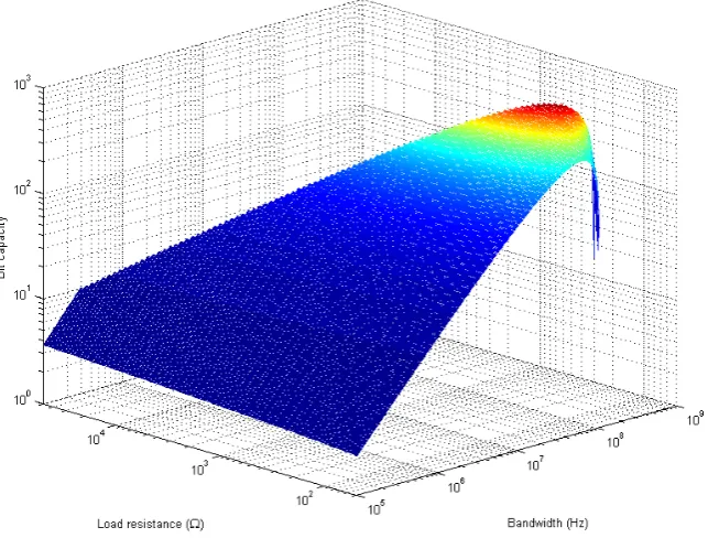
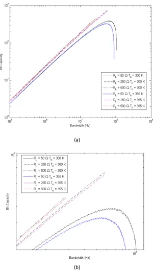
Fig. 3.1.6 Bit capacities for different load resistors and bandwidths ... 52
Fig. 3.1.7 Bit capacities of channels with load resistors 50 Ω, 250 Ω and 500 Ω ... 53
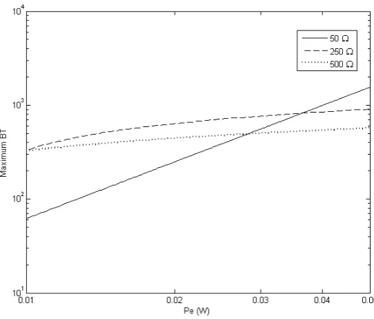
Fig. 3.1.8 Maximum bit capacities (BT) of channels with load resistors 50 Ω, 250 Ω and 500 Ω on emitter power from 10 mW to 50 mW ... 55
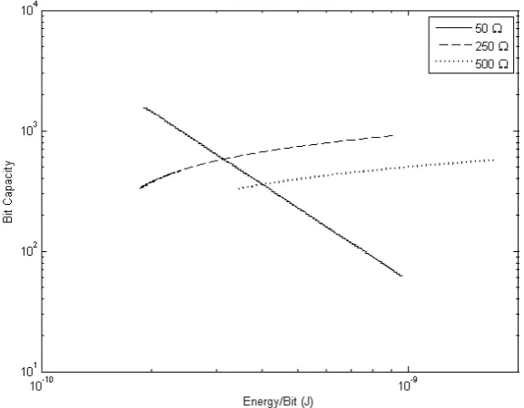
Fig. 3.1.9 Power efficiency distribution of maximum bit capacities of channels with load resistors 50 Ω, 250 Ω and 500 Ω ... 56
Fig. 3.1.10 Power and bandwidth combinations of channels with load resistors 50 Ω, 250 Ω and 500 Ω at bit rate of 20 kbit/s ... 56
Fig. 3.1.12 Distance effect of 50 Ω on bit capacity. ... 59
Fig. 3.1.13 Distance effect of 500 Ω on bit capacity. ... 59
Fig. 3.1.14 Bit capacity improvement from different effects compared to the benchmark channel ... 60
Fig. 3.2.1 Dynamic ranges of channels with load resistors 50 Ω, 250 Ω and 500 Ω with bandwidth ranging from 100 kHz to 100 MHz ... 63
Fig. 3.2.2 The model for the AGC amplifier ... 65
Fig. 3.2.3 The ideal relation of AGC amplifier voltages and communication session signal voltages ... 66
Fig. 3.2.4 The amplitudes of the Vin and Vout and K1Vin(min)Vc(max) in time ... 69
Fig. 3.2.5 AGC loop gain and delay ratio of channels with load resistors 50 Ω, 250 Ω and 500 Ω at a bit capacity of 50 bit ... 69
Fig. 3.2.6 A simplified transimpedance Op-amp amplifier model ... 70
Fig. 3.2.7 Equivalent circuit for the noise of the amplifier in Fig. 3.2.6 ... 71
Fig. 3.2.8 Simulation of TIA front end for Cf values given by (3.2.22) (red line) and (3.2.26) (blue line). For the details of the simulation, please see Appendix III) ... 74
Fig. 3.2.9 The frequency responses of g (blue line) and gn (red line) ... 75
Fig. 3.2.10 Noise frequency responses of TIA with different feedback resistors ... 76
Fig. 3.2.11 The performance comparison of TIAs and front end for different load resistors. Solid lines superposed on broken lines illustrate the performance of load resistor front ends when Rf = RL. 77 Fig. 3.2.12 Maximum bit capacities of channels with RL= 500 Ω, 5 kΩ (without TIA) and 50 kΩ and Rf= 500 Ω, 5 kΩ and 50 kΩ (with TIA) ... 78
Fig. 4.1.1 The hardware setup for demonstration of the windowed communication. ... 80
Fig. 4.1.2 A simplified geometry to model the received power of the experimental setup ... 81
Fig. 4.1.3 Definition of the geometric parameter of the hole projection approaching the photodiode collection area ... 82
Fig. 4.1.4 Comparison between the experimental setup and the theoretical model time varying power signal (the hole speed is 1/200 of the theoretical LED speed) ... 84
Fig. 4.1.5 Comparison between the fluctuations of the signal shown in Fig. 4.1.4 in the experimental and theoretical systems ... 85
Fig. 4.1.6 Distance factor versus simulation distance from 0.1 m to 1 m ... 88
Fig. 4.2.1 The components of IR transceiver circuit. (PD = photodiode, T-I = transimpedance and AGC = automatic gain control) ... 89
Fig. 4.2.2 The schematic of IR transmitter circuit ... 90
Fig. 4.2.3 The schematic of the TIA and pre-amplifier in the receiver ... 90
Fig. 4.2.4 The schematic of the AGC amplifier and threshold in the receiver ... 91
Fig. 4.2.5 The FET envelope detector ... 95
Fig. 4.2.6 Simulation result of the FET envelope detector. Red line: output of the detector; Blue line: AM signal input of the detector. ... 96
Fig. 4.3.1 The differences between a theoretical, an ideal and an actual threshold in AGC amplified signal. ... 97
Fig. 4.3.2 The dual detection identification. ... 98
Fig. 4.3.3 The system that generates eye diagrams to demonstrate the DDI function. ... 99
Fig. 4.3.4 Persist plot of system with DDI in Fig. 4.3.3 in 10 s at 200 kHz. ... 100
capacities. ... 103
Fig. 4.3.7 The bit capacities for the front end in Fig. 3.1.4 with 50 Ω load resistor and TIA in Fig. 3.2.6 with 50k Ω feedback resistor using OOK and 2mm OPPM that m = 2. ... 104
Fig. 4.4.1 The connections between the MSP430 microcontroller and the IR transceiver circuit ... 106
Fig. 4.4.2 Normal Workflow of DT and DR. ... 107
Fig. 4.4.3 Searching signal and frames definitions. ... 108
Fig. 4.4.4 A sample of the single timer A output mode 4 operation when in the up mode. ... 110
Fig. 4.4.5 Timer A and B alternative output workflow. ... 111
Fig. 4.4.6 Block diagram of the MSP430 microcontroller output program. ... 111
Fig. 4.4.7 Software latch function of DT ... 112
Fig. 4.4.8 Signal decoding and software latch function of DR. ... 113
Fig. 4.5.1 Signal amplitude during the rotation period; the presence of the signal indicated the time length of the transmission window simulated experimentally ... 115
Fig. 4.5.2 The interval measurement between two windows of the experimental setup... 116
Fig. 4.5.3 The one-channel setup for error rate estimation. ... 117
Fig. 4.5.4 The maximum gain of the AGC amplifier and BER of the channels with 5.1 kΩ and 51 kΩ resistors, in which G = gr1gr2(max). ... 118
Fig. 4.5.5 The measurements of the micro controller turnaround times. ... 119
Fig. 4.5.6 The voltage waveform of the 3.6 Ω series resistor. ... 122
Fig. 5.1.1 The model of a motor with basic components. ... 125
Fig. 5.1.2 The bundled and crossed over coils in a real motor ... 125
Fig. 5.1.3 The controlled meshing of the motor simulation. ... 128
Fig. 5.2.1 The magnetic flux densities. ... 130
List of Tables
Table 1 Comparison of the reviewed possible power supplies and solution ... 36
Table 2 The parameters used as the reference setup ... 51
Table 3 The feedback capacitors from (3.2.26) ... 76
Table 4 The MSP430 microcontrollers. ... 105
List of Publications
Huang, P., Iliescu D.D., Leeson, M.S. and Hines, E.L. Optical Wireless for Data
Abstract
A special application of optical wireless data transfer, namely on-line monitoring
and diagnostic of rotors in turbines and engines, has been considered in this thesis. In
this application, to maintain line of sight, i.e. data transfer, between a sensor placed on a
rotating component inside the turbine and a monitoring point placed in a fixed position
outside the turbine, a periodic fast fading channel is generated, which gives the
transceivers more flexibility regarding their mounting location. The communication in
such a channel is affected by the intermittency and variation of the signal power, which
produces a unique channel condition that influences the performance of the optical
transceiver.
To investigate the channel condition and the error rate of the periodic fast fading
channel with signal fluctuation, a model is developed to simulate the optical channel by
considering the variation of signal power as a result of the change in the relative
position of the photodiode with respect to the Lambertian radiation pattern of the LED,
in a simplified linear geometry. The error rate is estimated using the Saddlepoint
approximation on a specific threshold strategy. The results show that the channel can
afford the sensor data transmission and the performance can be improved by modifying
several parameters, such as geometrical distance, transmitter power and load resistor.
Compared to a normal channel, a higher load resistor on the photodiode front end has
the advantage of decreasing the noise level and increasing the data capacity in the fast
fading channel. The analysis of the automatic gain control amplifier indicates that a
higher load resistor needs a lower loop gain and from the model of the Transimpedance
amplifier (TIA), the bandwidth extension from the amplifier is more significant for a
higher resistor.
In addition to the theoretical model, an experimental setup is built to emulate the
channel in practice. The degree of similarity between the experimental setup and the
communication windows. Since it has been found that differences exist in the duration
of the communication window and the variation of the signal power, scaling factors to
ensure their compatibility have been derived. Transceiver hardware which
implemented the modelled functionality has been developed and a protocol to
establish the communication with the required error rate has been proposed. Using the
hardware implementation, a detection method for both rising and falling edges of the
signal pulses and a threshold strategy have been demonstrated. The device power
consumption is also estimated.
What is more, the electromagnetic environment of a squirrel cage motor is
simulated using the finite element method to investigate the interference and the
possibility of providing power to the IR communication devices using power
scavenging.
In the conclusion, the key findings of the thesis are summarised. A solution is
proposed for sensor data transfer using an optical channel for rotor monitoring
applications, which involves the design of the IR transceiver, the implementation of
the developed protocol and the power consumption estimation.
1
Introduction
This thesis presents the theoretical analysis and practical implementation of a
particular case of optical wireless (OW) communication channel, termed the periodic
fast fading channel, in which the Line-of-sight (LOS) channel between a pair of
transceivers is not persistent but appears and disappears periodically, caused by the
rotation of one transceiver relative to the other.
Typically, OW communications transfer signals in continuous LOS channels.
However, in some cases sustaining the LOS channel is difficult, especially for
applications in which the transceivers are in relative motion. One type of applications
in which such a situation arises is direct on-line monitoring and diagnostic of rotors in
generators and motors. In such applications, as wired communication is extremely
restrictive, wireless communication based on radio frequency (RF) signals has been
attempted. Compared to RF signals, optical signals have the advantage of reduced
susceptibility to Electromagnetic Interference (EMI) from the strong Electromagnetic
(EM) field present inside the generator or motor but suffer from the lack of a
continuous and reliable LOS channel. For these conditions, it is proposed that, if the
LOS channel is present intermittently, optical communication is still possible and
desirable, therefore a suitable solution should be found.
In the specific case of a generator in service, a point on the spinning rotor
appears in the same position repeatedly in each cycle of rotation. Thus, if the optical
transceiver placed on the rotor is pre-aligned with a transceiver in a fixed position,
such as on the stator or the casing of the generator, the transceivers can establish a
LOS channel when the position of alignment re-occurs in each cycle. In such a
condition, the LOS channel is limited to an extremely short period of time in each
1.1
System Description
The geometry of the system that creates the non-continuous LOS channel is
described schematically in Fig. 1.1.1. Two transceiver devices are necessary to
transfer the sensor data from the rotor, each named according to its main function as
the Data Transmitter (DT) and the Data Receiver (DR). The DT, located on the rotor,
collects and transmits data from the sensor and the DR, located on the stator, receives
the data from the DT for further analysis. When the DT is rotated to the position of
alignment in each rotation cycle, as shown in Fig. 1.1.1, a LOS channel can be
established for a short period of time when both optical receivers on the DT and the
DR are located in the of each other’s optical transmitters’ radiation patterns, as shown
in Fig. 1.1.2. The communication time in a cycle is determined mainly by the beam
width of the optical transmitter. The analysis of the effects of location and geometry
on the communication parameters will be discussed in section 3.1 and detailed further
[image:20.595.125.471.443.740.2]in Appendix I.
Fig. 1.1.1 The geometry of the intermittent fast fading channel
Data Transmitter
Data Receiver
Rotor
Fig. 1.1.2 The established LOS channel.
The dependence of the received signal power on the geometric parameters of the
optical transmitter generates a unique signal condition in the periodic fast fading
channel, compared to the typical optical channel in which the received signal power is
either constant or regulated. The rotation geometry impacts the received optical power
in the following two aspects:
1. When the optical transmitter and receiver are mounted in fixed positions on the
rotor and, respectively, the stator, the time proportion of the communication
relative to the rotation period remains constant. As the rotor accelerates and the
rotation speed increases, the actual communication time becomes shorter. If the
increased rotation speed results in a communication time that is insufficient for
one frame of the data transfer, the communication cannot continue.
2. The beam divergence of the optical transmitter, especially for a Light Emitting
specific location is determined by both angle and distance from the light source.
As the DT approaches, then departs the DR, the variation of angle and distance
between them introduces fluctuations in the signal power during the
communication time.
In summary, the signal power condition determines the performance of the fast
fading channel to a large extent.
What is more, since the DT has to be totally wireless due to the rotation, its
power has to be supplied from a battery or scavenged from the surrounding
environment and is, therefore, limited. The power efficiency of the DT should be
taken into account when estimating its performance.
1.2
Thesis Structure
The thesis is organised as follows:
Chapter 2 provides the research background for the project. The chapter starts
with an overview of the research and development of rotor monitoring and diagnostics
techniques and states the contribution of the present project to this field. Further
literature about Optical Wireless (OW) communication on fast fading channels is
reviewed. In addition, the power condition of the DT device on the rotor is analysed
and possible power supply and scavenging methods are introduced.
Chapter 3 includes the models that are developed to analyse the optical channel
parameters and the signal processing options for the fast fading channel, using a
simplified geometry. Performance and power efficiency parameters are derived from
the simulation and a special threshold strategy is introduced to evaluate bit capacity of
the channel for a specified error rate. The signal fluctuations are investigated and the
corresponding performance of an Automatic Gain Controlled (AGC) amplifier is
studied. Moreover, the influence of a Transimpedance Amplifier (TIA) on the
bandwidth of the channel is presented.
The rotating DT which creates the periodic optical channel is simulated in the
experimental setup by a rotating a disc with a hole, which allows optical access for a
small proportion of the disc’s period of rotation. The difference between the
experimental setup and the theoretical model is discussed and compared. A dedicated
signal detection method is developed to predict the signal condition and the influence
of the reduction in the modulation amplitude on the bit capacity is evaluated. The
design of the communication devices, including hardware and software, is described.
The channel performance results obtained from the experimental setup are discussed.
At the end of the chapter, further developments based on the results will be proposed.
Chapter 5 includes a Finite Element Method (FEM) model using a stationary
solver of a motor EM environment that investigates the interference and power
harvesting from the EM source, in which the theory, design and results of the model
are presented.
Chapter 6 is the conclusions of the thesis, providing the solution for the data
2
Background and Literature Review
2.1
On-line Rotor Monitoring and Diagnostics
The health of the rotor influences the performance of the motor or generator
directly, therefore in current years, rotor monitoring and diagnostics received great
interest from researchers. Due to the working condition of the rotor, sensor data for
parameters such as temperature, current and voltage of the winding [1], cannot be
easily transferred on-line. As a result, indirect monitoring methods that do not require
detection on site or installation of detectors inside the machine have received
significant attention. However, as RF and OW techniques are introduced for data
transfer, direct monitoring and diagnostics have the advantages of real-time monitoring
of rotor health, such as enhanced understanding of operating conditions and advanced
warning if some operating limits are exceeded [2, 3].
2.1.1
Indirect Methods
Indirect rotor monitoring and diagnostics uses parameters from other easy access
sources, such as current, voltage and resistance, to estimate the condition or defect of
the rotor. Specific data analysis algorithms or modelling are necessary because the data
does not indicate the rotor condition in a direct manner.
Current and voltage are the two most common references in rotor monitoring. One
of the examples is the additive frequency component from the broken rotor bars to the
current [4]. The related signal processing techniques for frequency analysis to detect
the side band can vary depending on the mathematical operation [5, 6]. For a more
accurate analysis that tolerates the disturbance from load and speed, the Vienna
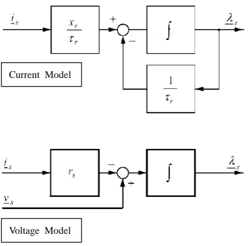
method has been investigated [7-9], in which two models, namely the current and the
In the current model the rotor flux linkage 𝜆𝑟 is calculated from the stator current 𝑖𝑠, the rotor reactance 𝑥𝑟 and time constant 𝜏𝑟, in which 𝑥𝑟 and 𝜏𝑟 is derived from a fixed reference frame of the rotor and 𝑖𝑠 is derived from measurement. The current model is used as reference. In the voltage model, the stator flux linkage 𝜆𝑠 is derived from stator current 𝑖𝑠, stator voltage 𝑣𝑠 and stator resistance 𝑟𝑠. As 𝑖𝑠 and 𝑣𝑠 of the voltage model are from measurement, the rotor faults affect the flux density and
the flux linkage, therefore can be found by comparing to the current model.
[image:25.595.182.429.269.512.2]Adapted from [7] Fig. 2.1.1 Current and Voltage Models of the Vienna Method
What is more, the rotor temperature can be estimated from the rotor resistance [10,
11], that can be formulated as:
𝑅2 =𝑅1𝜃𝜃2+𝑘
1 +𝑘 (2.1.1)
in which 𝑅1 and 𝑅2 are the resistances at temperatures (in degrees Celsius) 𝜃1 and respectively 𝜃2 and 𝑘 is the temperature coefficient of the material. As some of the motors and generators are provided with cooling mechanisms, temperature models
Current Model
include the effect from outer cooling by acquiring more parameters such as the stator
current and voltage [12], or by combining measurements with parameter estimations
[13]. Last but not least, a feedback based method by emitting acoustic waves for
detecting friction faults that caused from vibrations can be found in [14].
Data from indirect rotor monitoring methods are usually derived and compared to
a standard model that represents the normal condition, and a fault or defect is indicated
if the data does not agree with the standard model. The monitoring algorithm can be
implemented using standard computers or dedicated Digital Signal Processors (DSPs).
The interface can be either local [15] or remote, such as over the Internet, realized by
publishing the data acquisition server online [16]. Using computer assisted
optimization design, the monitoring algorithm can be implemented on a
Field-program Gate Array (FPGA) [17]. DSPs can be used for data processing either
as signal interpreters for further processing [18] or as individual diagnostic systems
[19]. Specific signal processing DSP chips, such as fuzzy logic [20] or discrete
wavelet transform [17] can also be included. To add more intelligence and flexibility,
artificial neutral networks have also been trained to detect rotor faults [21].
2.1.2
Direct Methods
Values of key parameters for rotor health can be acquired by sensors. With
dedicated data transfer technology, the real time status of the operational rotor can be
shown instantly with considerable accuracy. However, the difficulty of the direct
monitoring using sensors is the implementation of data transfer from the rotating
component to a component with no movement.
Compared to indirect methods, the number of monitoring parameters for direct
methods is significantly reduced, for example in most cases, only one parameter (e.g.
temperature) is needed. Current research shows great interests for temperature and
vibration sensing [22-30]. In exceptional cases other parameters can also be
measured. In [31] the rotor current is measured without sensors to diagnose the
an easy setup that is mounted entirely on the shaft, with no other component mounted
inside the machine frame on the rotor.
The data transfer technologies for direct rotor monitoring can be divided into
three main categories, defined by the different signal carriers: contact, RF and optical.
The rotor current measurement described in [31] uses slip rings to maintain metal
contact between devices. A near field rotary transformer system is found in [33],
which leaves a narrow air gap between the rotary and stationary modules of the
antenna, therefore the power and electric signals are both transmitted without
significant loss. RF communication is used for different applications, depending on
the system configuration and required bandwidth. Rotor vibration sensor signals are
directly modulated on RF signals, using a simple signal convertor [22]. A more
general RF solution is summarized in Fig. 2.1.2, where the RF communication is
performed by dedicated chips, which transform the sensor signals into RF signals that
are specific to different protocols. Microcontrollers can be added to manage the data
acquisition and conversion, therefore providing more options for the RF protocols
(Route 1 and 2 in Fig. 2.1.2).
Fig. 2.1.2 A common RF solution for direct rotor monitoring. (Route 1: sensors → microcontroller
→ RF communication chip → antenna. Route 2: sensors → RF communication chip → antenna. Route 3: sensors → microcontroller → antenna.)
Examples of different techniques are the higher bandwidth ZigBee [23, 32] and
WiFi [24] protocols, short range wireless Bluetooth [25] and RFID-S [26]. The
power consumption and extra packet loss[27]. As a substitution, OW methods are
used. The same configuration from Fig. 2.1.2 is also applied for data transfer using
OW signals, where the LED and photodiode represent the optical antennas and the
data transfer can be accomplished only by a microcontroller (route 3 in Fig. 2.1.2).
Direct transmission on an infrared channel of digital signals from sensor data is
demonstrated in [29], in which the received IR data needs to be re-formatted to adapt
to the RS-232 interface. Differently, in [30] the IrDA Serial Infrared (SIR) protocol is
introduced and the DR is not necessarily specially designed. In addition, an optical
channel can be used for other purposes than data transfer, such as in a passive sensing
application, presented in [34], in which the rotor temperature is detected by
processing the optical fibre sensor reflection of the incoming optical signal.
The devices located on the rotor for contactless monitoring applications are
completely isolated from the constant power supplies. Two power solutions presented
in the literature have been reviewed in this section. Batteries of different kinds are
stated in [22, 25, 27, 29, 32] as the power source. However, for some applications
such as torque measurement [32], batteries cannot provide the solution for long-life
power and power scavenging represents a better solution. Alternatively, wireless
power supplies are described in [26, 28, 35], in which the power transformers convert
and transmit power in AC coupling. The block diagram of the transformer
demonstration from [35] is shown in Fig. 2.1.3.
In this diagram, the DC power supply of the device on the rotor is transferred and
converted from the frequency raised power through two windings, from a normal 50
Hz supply. Analysis of the AC coupling power efficiency and corresponding
simulation of a pair of ring shaped coupling coils is performed in [26]. The results
indicate that with proper shielding, the power loss caused by eddy currents can be
significantly reduced. Moreover, special design for low power consumption is
required on the communication devices that uses wireless AC coupling power transfer
in these cases, and from the literature, this technique does not appear in applications
using OW transfer, which generates the uncertainty of whether the OW devices can
sustain a long time transmission from an alternative power source other than using
batteries.
Mounting locations of the wireless sensor data transfer devices using RF or OW
on the rotor are restricted in order not to compromise the rotation. The location of the
rings for power transfer of the RF data transfer device using AC coupling is discussed
in [26]. The non-stop power supply is established by concentrically rotating one ring
with the rotor. A similar problem exists in the OW applications when preserving the
continuous optical LOS channel. Generally, constructing a constant link for power or
optical signal between the device on the rotor and the one on the stator requires a
special setup or positioning. In [29] and [30], the IR transmitter on the rotor is mounted
on the shaft stub, as shown in Fig. 2.1.4
From [30]
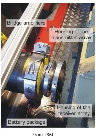
Alternatively, the optical antenna with IR LED array is clamped around the shaft
body [36], as shown in Fig. 2.1.5.
[image:30.595.206.412.143.434.2]From [36]
Fig. 2.1.5 IR transmitter clamped on the shaft body. The transmitter ring and receiver ring produce a continuous link in the rotation circle.
2.1.3
Summary
Rotor monitoring and diagnostic methods, including the corresponding necessary
parameters, modelling, data processing and transfer are presented in this section.
Using indirect methods to detect broken bars and temperature share the advantage of
no access to the interior of the machine, but needs more resource for data processing
and modelling. For direct methods, temperature and torque sensing data are acquired
and transmitted from a device on the rotor to a device in a fixed position. While
wireless communication techniques, such as RF and OW, are introduced in the
application. Problems with the power supply and LOS channel of OW are generated
imposed on the mounting location of the devices, which involve AC coupling wireless
power transfer technique for DT device on RF communication and continuous LOS
channel on OW channel; batteries are used as the power supplies for most of the
reviewed applications to overcome the problem of powering the device installed on
the rotor.
2.2
Short Distance Wireless Infrared Communication
OW communication has been applied for short distance applications such as
WLAN and other networks for indoor communications [37-40]. Some of the benefits
of using OW instead of RF result from no RF frequency band occupation, freedom on
the use of the spectrum without regulation and lower cost [41, 42]. Another benefit for
the OW is the resistance to EMI for industrial applications in which the environmental
EMI is strong [43] or close to a known EM field sources such as motor or generators
[44-46]. The EMI influence on optical transceiver circuits has been investigated in
[47, 48]. Successful industrial applications of OW have been described in section 2.1,
with more examples of rotor health monitoring found in [36, 49, 50].
Long distance OW communications need to consider the environmental
influences such as beam dispersion and attenuation due to the atmosphere [51]. The
scatter effect from the atmosphere can be estimated using the model in [52]:
ascatt ≅17S ∙ �555λ � 0.195∙S
(dB/km) (2.2.1)
in which S is the human eye visibility, λ is the wavelength of the infrared signals. In the short distance scenario, such as indoor communications, the scatter from
(2.2.1) can be ignored for a communication distance of less than 1 m. There are two
types of indoor channels: LOS and non-LOS, as shown in Fig. 2.2.1. The signal
reception range from a non-LOS channel may be improved by reflecting the optical
signals, but the loss from the reflection is also considerable. What is more, the loss of
Lambert’s law, therefore significant [53, 54]. In consequence, LOS channels are
preferred in practice, especially for applications using LED where the radiation angle
is much wider than that of a laser diode.
From [53] Fig. 2.2.1 Indoor optical communication channels
2.2.1
Photodiode Signal Response
In an optical receiver where a P-i-N photodiode is the optical to electronic signal
convertor, the bottleneck of the performance is from the diode capacitance that limits
the bandwidth. Depending on the bias voltage, the response of a photodiode is
different. In response to an optical signal, applying reverse bias to the photodiode
produces a photoconductive current signal, while a photovoltaic voltage signal is
generated with no bias.
A two-valley model of the photodiode photoconductive current response can be
found in [55-61]. The equivalent circuit of a simplified model based on step function
for the response of the pulse [55] is shown in Fig. 2.2.2.
The voltage 𝑈(𝑡) is given by:
in which 𝑉𝐶𝐶 is the bias voltage, 𝑅 is the load resistor and 𝑅 is the diode capacitance, and the generated current from the photodiode 𝑅(𝑡) is mainly from photo current:
𝑅= 𝑞𝑞′𝑃ℎ𝑓𝑑𝑅
𝑖 �𝑣𝑛𝑛+𝑣𝑝𝑝� (2.2.3)
in which 𝜇 is the mobility of electrons and holes in the corresponding valley accordingly, 𝑛 is the electron concentration and 𝑝 is the hole concentration, 𝑉𝑑 is the punch-through voltage, 𝑣𝑛 and 𝑣𝑝 are the velocities of electrons and holes:
𝑣𝑛,𝑝 =𝜇𝑛,𝑝(𝑈 − 𝑉𝑑 𝑑
𝑖 ) (2.2.4)
and 𝑞′ is a coefficient from the photodiode quantum efficiency 𝑞:
𝑞′ = 𝑞
(1− 𝑒−𝛼𝑑𝑖) (2.2.5)
Adapted from [55]
Fig. 2.2.2 Equivalent circuit of the photodiode photoconductive model
of a pulse in the form of the step function ℎ(𝑡 − 𝑡1)− ℎ(𝑡 − 𝑡2) is:
𝑛(𝑡) =� [ℎ(𝑡0− 𝑡1) 𝑑/𝑣𝑛
0
− ℎ(𝑡0− 𝑡2)]�1− 𝑒−𝛼𝑑𝑖𝑒𝛼𝑣𝑛(𝑡−𝑡0)�𝑑 𝑡0
(2.2.6)
𝑝(𝑡) =� [ℎ(𝑡0− 𝑡1) 𝑑/𝑣𝑝
0
− ℎ(𝑡0− 𝑡2)]�𝑒𝛼𝑣𝑝(𝑡−𝑡0)−𝑒−𝛼𝑑𝑖�𝑑 𝑡0
(2.2.7)
What is more, the photodiode photoconductive response in time 𝑅(𝑡) also includes the components of the displacement current. From this model, the expression for 𝑅(𝑡) can be simulated in software, which is based on the approximation of the electron and
hole concentrations.
2.2.2
Noise Condition
Noise sources for short distance OW communication are mainly from the
receiver front end, which produces Gaussian noise, shot noise and excess noise in
general.
The noise from the electrical circuit of the photodiode front end is considered as
thermal noise caused by the random thermally excited vibration of the charge carriers in
a conductor, which exists in a conductor with a temperature above absolute zero [62,
63]. The thermal noise appears in any circuit component with resistance and can be
evaluated in the Johnson–Nyquist noise model [64]. The available noise power is
proportional to the bandwidth and temperature, which is:
in which 𝑘= 1.38 × 10⁻²³ J/K is the Boltzmann’s constant, 𝑇𝑛 is the equivalent noise temperature and ∆𝑓 is the noise bandwidth of the measuring system. The equivalent circuits are shown in Fig. 2.2.3, in which the noise is considered being the current
source 𝑖𝑛 in the Thevenin model or the voltage source 𝑈𝑛 in the Norton model.
Adapted from [63] Fig. 2.2.3 Thermal noise equivalent circuits
The corresponding current and voltage equations are:
𝑖𝑛 =�4𝑘𝑇𝑅𝑛∆𝑓 (2.2.9)
𝑈𝑛 =�4𝑘𝑇𝑛𝑅∆𝑓 (2.2.10)
where 𝑅 is the resistance. If the noise power per Herz is constant over the entire bandwidth, the thermal noise can be treated as ‘white’ noise. When the noise is
approximated by a Gaussian distrubution, the variance 𝜎2 of the noise current is the product of the power spectral density 𝑆 and the bit time 𝑇 [65, 66]:
Thevenin model
𝜎2 = 𝑆𝑇
=2𝑘𝑇𝑅𝑛𝑇 (2.2.11)
In signal processing, the noise is usually filtered and reduced. The filtered
Gaussian noise is no longer white in spectrum. In this case, the power spectral density
depends on the frequency response of the filter 𝐻(𝑓) [66]:
𝑆=�∆𝑓2𝑘𝑇𝑛|𝑅𝐻(𝑓)|2
0 𝑑𝑓
(2.2.12)
Another method to estimate the power spectral density is suggested in [67]. What
is more, a transient noise model is discussed in [68] where the frequency dependent
noise is included.
In addition, amplifiers introduce noise to the amplified signals. According to
[69], the noise from the operational amplifier as pre-amplifier can be modelled as
noise of 1/f characteristic that is given by the impedance frequency poles of the
photodiode and amplifier circuit network. Various models are found to estimate the
Op-amp noise that is from the inputs, in which [70, 71] take into account the
correlation of the equivalent noise current input spectra and the equivalent noise
voltage.
Noise is generated not only on electronic signals but also on signal conversion
from optical to electronic. For example, shot noise appears in the converted electronic
signals of the photodiode due to the random arrival of the photons [66]. Modelling the
discrete stochastic events of the photon electrical response as a Poisson distribution,
the ordinary photodiode current is derived [72, 73]:
𝑅(𝑡) =� 𝑔(𝑡 − 𝑡𝑖) 𝑖
in which 𝑡𝑖 represents the random occurring time of the photoelectric signal 𝑔(𝑡) from the absorption of a photon. Generally speaking, different formats for the noise
𝑔(𝑡) produce different shot noise; in Fig. 2.2.4 some examples are shown.
Adapted from [73] Fig. 2.2.4 Shot noise shaping examples (𝑔(𝑡)).
Considering the photodiode response, therefore:
� 𝑔∞ (𝑡)
−∞ = 𝑞
(2.2.14)
in which 𝑞 is the electrical charge. The average shot noise current is suggested in [74]:
𝑅𝑛2 = 2𝑞(𝑅+𝑅𝑑)∆𝑓 (2.2.15)
where 𝑅 is the photodiode signal current and 𝑅𝑑 is the dark current.
If an Avalanche Photodiode (APD) is the photoelectric converter of the receiver,
76]. From (2.2.13), the Poisson shot noise current with the random avalanche gain 𝑎𝑖 becomes:
𝑅(𝑡) =� 𝑎𝑖𝑔(𝑡 − 𝑡𝑖) 𝑖
(2.2.16)
The noise factor of excess noise in the APD is [77, 78]:
𝐹𝑒(𝑀) =𝜅𝑀+�2−𝑀�1 (1− 𝜅) (2.2.17)
𝐹ℎ(𝑀) =𝑀𝜅 +�2−𝑀� �1 1−1𝜅� (2.2.18)
where 𝐹𝑒(𝑀) represents the electron injection, 𝐹ℎ(𝑀) represents the hole injection, 𝑀 is the multiplication factor and 𝜅 is the electron initiated multiplication.
2.2.3
Signal Amplification for the Receiver Front End
Electronic signals converted from optical photons by the photodiode are usually
too weak to be processed directly. As described in section 2.2.1, the photodiode
frequency response is limited by the diode capacitance. Thus, the electronic signal
amplifier for the photodiode front end has two functions: to amplify converted
electronic signals at the photodiode front end and to compensate for the influence of
the diode capacitor and extend the communication bandwidth. According to [79], two
types of amplifier are able to perform these two functions, namely the TIA and the
bootstrap amplifier. Considering a demonstrative amplifier solution, the TIA is more
preferred to the bootstrap amplifier for the initial design. As the bandwidth of the TIA
is limited by the open loop gain of the operational amplifier component [80],
bootstrap amplifier may allow more bandwidth. However, both the bootstrap
increase the instability. What is more, bootstrap amplification can be combined in TIA
to increase the bandwidth [81].
Moreover, due to the fact that the LED and the photodiode are in relative motion
when the transceivers are connected to the optical channel in this application,
fluctuations appear in the received signals, where an AGC amplifier is needed for the
reduction of the fluctuation.
One example of a TIA which has been used in [82] and [83] is shown in Fig.
2.2.5.
Adapted from [79]
Fig. 2.2.5 Example of TIA, in which 𝑅𝑝ℎ is the photodiode current, 𝑅𝐷 is the diode capacitance,
𝑅𝑆𝑆 is the shunt resistor, 𝑅𝑓 is the feedback resistor and 𝑅𝑓 is the feedback capacitor
The gain 𝑔𝑚 of the amplifier is given by [82]:
𝑔𝑚 =−𝑅𝑓�1 +𝐴𝑂𝑂𝐴
𝑂𝑂� (2.2.19)
in which 𝑅𝑓 is the feedback resistor and 𝐴𝑂𝑂 is the Op-amp open loop gain. When 𝐴𝑂𝑂>>1, the amplifier gain is approximately equal to −𝑅𝑓. However, 𝐴𝑂𝑂 decreases at higher frequency and reaches 0 dB when the frequency is equal to the GBW of the
Op-amp [84]. As a result, the Op-amp limits the performance of the TIA. What is
with the feedback resistor and has a lower cut off frequency than that of the GBW as
will be shown using a model of a simple TIA in Chapter 3.
The DC photon current may affect the TIA performance, in this application, the
influence of DC photo current may not affect the performance to a level that needs to
be compensated at the expense of power on additive components. If the influence is
significant, the improved designs to reject DC photo current using active feedback
loop can be found in [82, 85].
The AGC amplifier is an nonlinear system, for which two analytical models, one
with and one without a logarithmic converter, are described in [86]. The generic AGC
amplifier components for both models are shown in Fig. 2.2.6.
Fig. 2.2.6 Analytical model for the AGC amplifier
The gain control depends on the relationship between the gain of the Variable
Gain Amplifier (VGA) and the control voltage 𝑉𝑐.
In the model with logarithmic converter, the gain of the VGA is:
𝑔𝑉𝑉𝑉 =𝐾1𝑒𝑎𝑉𝑐 (2.2.20)
𝑉𝑜𝑜𝑡 = 𝑉𝑖𝑛𝐾1𝑒𝑎𝑉𝑐 (2.2.21)
Using a logarithmic converter between detector and 𝑉𝑑, the transfer function between 𝑉𝑜𝑜𝑡 and 𝑉𝑑 is:
𝑉𝑑 =𝑙𝑛 (𝐾𝑒𝑉𝑜𝑜𝑡) (2.2.22)
where 𝐾𝑒 is the gain of the envelope detector. So 𝑉𝑐 is related to 𝑉𝑜𝑜𝑡 by:
𝑉𝑐 =𝐹�𝑉𝑟𝑒𝑓− 𝑉𝑑�
=𝐹�𝑉𝑟𝑒𝑓 − 𝑙𝑛 (𝐾𝑒𝑉𝑜𝑜𝑡)�
(2.2.23)
in which 𝐹 is the response of the low-pass filter. These specific components compose an AGC amplifier that is linear in a decibel scale, which is:
𝑙 𝑛�𝑉𝑜𝑜𝑡�1 +𝑎𝐹(𝑠)��=𝑙𝑛𝑉𝑖𝑛+𝑉𝑟𝑒𝑓𝑎𝐹(𝑠) (2.2.24)
The decibel linearity also exists in a square-law detector that is modelled in [87],
which defines the 𝑉𝑑 of the logarithmic converter response from 𝑉𝑜𝑜𝑡 as:
𝑉𝑑 =𝑘2𝑙𝑛 �𝑉0 2
𝑘1� (2.2.25)
in which 𝑘1 and 𝑘2 are the constants of the logarithmic converter. A similar model containing more details of the AGC amplifier with logarithmic converter can be found
in [88], which describes the settling time of this amplifier model.
If the logarithmic converter is not implemented in the AGC amplifier, the decibel
and 𝑑𝑉𝑖𝑛
𝑉𝑖𝑛 [86], based on which an iterative analysis is discussed in section 3.2.2.
Modelling and design of the AGC amplifier with no decibel linearity is also described
in [89]. What is more, [90, 91] uses the loop gain from 𝑉𝑟𝑒𝑓 to 𝑉𝑜𝑜𝑡 to analyse the AGC amplifier. Since 𝑉𝑐 generates positive feedback to the system, the studies of the resonance properties in [89] and [91] give the natural frequency 𝜔𝑛 and the damping factor ξ𝑑 as:
𝜔𝑛 =�𝐾1𝐾2𝐾𝑑𝑞𝑒 (2.2.26)
ξ𝑑 = 𝑝
2�𝐾1𝐾2𝐾𝑑𝑞𝑒 (2.2.27)
In which 𝑝𝑒 and 𝑞𝑒 are constants of the envelope detector transfer function:
𝐻𝑒(𝑠) =𝑠𝐾+𝑑𝑞𝑝𝑒
𝑒 (2.2.28)
2.2.4
Signal Modulation
The signal modulation for indoor short distance optical communication channel
with direct detection can be analogue or digital. Amplitude modulation is excluded
from this discussion, since, in this application, large fluctuations exist in the
amplitude of the original signal. According to [92], other available modulation
techniques are Frequency Modulation (FM), Frequency Shift Keying (FSK) and
Phase Shift Keying (PSK), as examples of analogue modulation techniques, and On
Off keying (OOK) and Pulse Position Modulation (PPM) as examples of digital
modulation techniques. The transferred data and corresponding optical signals of FSK
Adapted from [100]
Fig. 2.2.7 Examples of transferred data and corresponding optical signals of (a) PSK and (b) FSK
Early research of FSK in OW communications can be found in [93, 94] for
multi-channel WLAN applications. PSK with a subcarrier has been investigated in
[95, 96]. Thus, the channel reuse is an advantage of FSK and PSK. In an underwater
application from [97], PSK can achieve higher data rate when compared to digital
modulation, however, at the same time has the worst power efficiency. Moreover,
PSK and FSK are also considered highly difficult to implement. In addition,
Orthogonal Frequency-division Multiplexing (OFDM) became popular in optical
communication recently because of the increase in bandwidth demand and the
development of DSP that provides faster signal processing for OFDM [98].
In this application, the benefits of FSK, PSK and OFDM which come from
channel reuse result in the capability to transmit more data during the limited
communication period. This becomes important when the communication time of the (b) FSK
fast fading channel is not sufficient to transfer all the sensor data or the data comes
from multiple sensors and needs to be transferred in one channel. However, the poor
power consumption cannot be ignored, and, coupled with the implementation
complexity, power efficiency may be further depressed on extra energy spent on the
physical layer of the modulation (hardware). Considering power is more essential than
a higher data rate for the application, digital modulation is preferred.
Digital modulation techniques are well developed for OW communications. One
of the successful examples is the IrDA standard using OOK and PPM at different bit
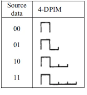
rates [99, 100]. Besides those two modulations, Digital Pulse Interval Modulation
(DPIM) is a potential substitution of PPM, which eliminates unused time slots in PPM
to gain higher transmission efficiency [101].
Based on the arrangement and number of pulses in a symbol as well as the
symbol length, there are at least three major PPM schemes, namely traditional PPM
(1-PPM), Multi PPM (MPPM) and Overlapped PPM (OPPM) [102, 103]. In a symbol
period 𝑇𝑠 that is sliced into 𝑛 sub-slots, in 1-PPM only one slot is occupied by the signal pulse in those slots, in which the pulse interval is 𝑇𝑠
𝑛. The pulse occupation of
symbol slots on MPPM and OPPM are both more than one. The slots in use are not
constrained and can be arbitrary in MPPM, while in OPPM those occupied slots are
joint. What is more, more symbols can be generated if the total amount of slots can be
different of 1-PPM and OPPM, namely Differential-PPM (DPPM) and Differential
Overlap-PPM (DOPPM) [102, 104], and a combination scheme of MPPM and pulse
width modulation is discussed in [105]. What is more, the modulation can be on the
interval of the pulse, a symbol example of a digital pulse interval modulation with 4
symbols (4-DPIM) scheme is shown in Fig. 2.2.8, the difference between the symbols
is from the amount of unoccupied slots. The pulse of DPIM can also be used for
Adapted from [106] Fig. 2.2.8 Example of 4-DPIM scheme without guarding slot
The power performance of the above modulations are compared with OOK as a
benchmark in several references [102, 106, 107], in which the power ratio of one
modulation over OOK in the same bit rate and Bit Error Rate (BER) is approximately
the ratio of the minimum Euclidean distance between the two nearest symbols of the
modulation over that of the OOK. As a result, the power ratios are:
𝑃𝑃𝑃𝑃 𝑃𝑂𝑂𝑂 =�
2
𝐿log2𝐿
(2.2.29)
𝑃𝑃𝑃𝑃𝑃 𝑃𝑂𝑂𝑂 =
2𝑚
�𝑛𝑑log2𝐿 (2.2.30)
𝑃𝑂𝑃𝑃𝑃 𝑃𝑂𝑂𝑂 =
2𝑚
�2𝑛log2(𝑛 − 𝑚+ 1)
(2.2.31)
𝑃𝐷𝑃𝐷𝑃 𝑃𝑂𝑂𝑂 =
4�𝐿log+ 1 2𝐿
(𝐿+ 3)√2
(2.2.32)
in which 𝑃(𝑚𝑜𝑑𝑜𝑚𝑎𝑡𝑖𝑜𝑛) represents the average power of the modulation, 𝐿 is
is the total amount of symbols selected for the modulation scheme, 𝑚 is the number of occupied slots in MPPM and OPPM, and 𝑑 is the minimum Hamming distance between MPPM selected symbols. From the results in the literature [102, 106, 108], in
a general manner the power requirement rating of the modulations can be summarized
as OPPM > OOK > 1-PPM > DPIM > MPPM. The exact power depends on the
preference of 𝐿, 𝑛 and 𝑚. The selection and power analysis of the modulation for the fast fading channel will be presented in section 4.3.
2.2.5
The IrDA Standard
IrDA is a short distance wireless infrared communication standard for point to
point half duplex communication released by the Infrared Data Association, dating
back to 1993 [92]. From then on, the officially stated milestones of the IrDA
development on data rates were: 4 Mbits/s in 1994, 16 Mbits/s in 1999 and 1 Gbits/s
in 2009 [109]. As mentioned in section 2.1.2, the device in [30] has been developed
for data transfer of rotor monitoring using the IrDA protocol. A considerable
advantage of adopting this off-the-shelf technique is reducing the effort and
uncertainty of the hardware development. This section investigates whether IrDA can
be implemented on the fast fading channel.
The IrDA protocol has now developed beyond the early function of cable
replacement into an application dependent wireless platform [110]. The protocol plays
the role of interfacing between the user application and the wireless infrared
communication, as can be shown from the summarized IrDA architecture in Fig. 2.2.9
[110-112]. According to the Infrared Data Association, the functions of the core layers
are briefly described as [111]:
Information Access Service (IAS): advertisement and discovery for remote
devices
Infrared Link Multiplexing Protocol (IrLMP): multiplexing services
Infrared Link Access Protocol (IrLAP): link management
Physical Layer: specification of physical devices
The physical layer can be further divided, based on the data rate, into: SIR up to
115.2 kbit/s, Medium Infrared (MIR) up to 1.2 Mbit/s and Fast Infrared (FIR) at 4
Mbit/s [116, 117]. Other layers, such as Object Exchange (OBEX), Infrared
Communication (IrCOMM) and Tiny Transport Protocol (Tiny TP), are application
specific and redirect the data to the targeted destination [112].
Fig. 2.2.9 A summarized IrDA architecture, with optional layers marked blue.
From the protocol introduction above, upper layers of the IrDA protocol define
the interface of wireless infrared communication to different software applications. To
investigate the possibility of using IrDA in this application, the IrLAP layer is
considered at first to find if there is any conflict between the specific channel
condition and the IrDA optical standard concerning throughput efficiency and burst
transmission.
In general, the data rate of IrDA is sufficient for the intermittent communication
in this application as it exceeds 1 Gbit/s. Even if the available communication period
is only 1/1000th of a rotation cycle, the overall data rate is reduced from 1 Gbit/s to 1
Mbit/s. However, a high data rate may not result in high information rate when taking