warwick.ac.uk/lib-publications
Original citation:
Rajaguru, Pushparajah , Ortiz-Gonzalez, Jose Angel , Lu, Hua, Bailey, Chris and Alatise,
Olawiwola. (2017) A multiphysics modeling and experimental analysis of pressure contacts in
power electronics applications. IEEE Transactions on Components, Packaging and
Manufacturing Technology, 7 (6). pp. 893-900.
Permanent WRAP URL:
http://wrap.warwick.ac.uk/97638
Copyright and reuse:
The Warwick Research Archive Portal (WRAP) makes this work by researchers of the
University of Warwick available open access under the following conditions. Copyright ©
and all moral rights to the version of the paper presented here belong to the individual
author(s) and/or other copyright owners. To the extent reasonable and practicable the
material made available in WRAP has been checked for eligibility before being made
available.
Copies of full items can be used for personal research or study, educational, or not-for profit
purposes without prior permission or charge. Provided that the authors, title and full
bibliographic details are credited, a hyperlink and/or URL is given for the original metadata
page and the content is not changed in any way.
Publisher’s statement:
“© 2017 IEEE. Personal use of this material is permitted. Permission from IEEE must be
obtained for all other uses, in any current or future media, including reprinting
/republishing this material for advertising or promotional purposes, creating new collective
works, for resale or redistribution to servers or lists, or reuse of any copyrighted component
of this work in other works.”
A note on versions:
The version presented here may differ from the published version or, version of record, if
you wish to cite this item you are advised to consult the publisher’s version. Please see the
‘permanent WRAP URL’ above for details on accessing the published version and note that
access may require a subscription.
Abstract— This paper details a modelling and experimental assessment of the packaging process for a silicon carbide Schottky diode using pressure contacts. The work detailed in this paper is original as it applies a combined electro-thermo-mechanical modelling analysis to this packaging method supported by experimental validation.
A key design objective for this packaging process is to identify suitable contact pad materials, heat-sinks, and process variables such as clamping force to meet electrical, thermal and reliability specifications. Molybdenum and Aluminum Graphite have been identified as two suitable materials for the contact pads. Clamping forces ranging from 300 to 500N and electric current ranging from 10A to 30A have been investigated in terms of the resulting electrical and thermal contact resistances, temperatures, and stresses induced across the package. The performance of two heat sink designs with heat dissipation rates of 12893 W/m2k and 4991 W/m2k have also been investigated.
Both the modelling and initial experimental results detailed in the paper show that Aluminum Graphite provides better performance in terms of generating a lower average chip temperature. Both temperature and stress in the diode are predicted as a function of clamping force and load current. This will aid the packaging engineer to identify suitable process parameters to meet junction temperature requirements at different applied load currents.
Index Terms—Press-pack, diode, power electronic module.
I. INTRODUCTION
In this paper we present a multi-physics (electro-thermal-mechanical) modelling analysis is presented and compared with experimental results for a press pack diode (PPD) in a power electronic module (PEM) applications. The thermo-mechanical characteristics of the pressure contact packaging system offers certain advantages since the majority of the failure mechanisms in power electronics modules are associated with bonded joints such as solder joints and wirebonds [1]. Eliminating both wirebonds and solder joints helps to minimize the risk of fatigue failure, and hence providing an enhanced reliability.
In a press-pack module, (also named as flat pack in some of the literature), the power semiconductor is pressed between two
1 Computational Mechanics and Reliability Group, Department of
Mathematical Sciences, University of Greenwich, Old Royal Naval College, Park Row, London, SE10 9LS
conductive copper elements using an intermediate contact material to match the Coefficient of Thermal Expansion (CTE) of the copper and the semiconductor. The press-pack module is assembled and mounted under pressure by a complex mechanical system [2] in order to obtain the necessary pressure contact between the interfaces in the package. Other advantages of press pack assembly in power electronics applications are compact design, double sided cooling, and reduction in rigid interconnection between materials of different CTE [3]
[image:2.595.306.551.420.497.2]In contrast to fully bonded interfaces such as solder joint and wirebond, press pack interfaces introduce additional electrical and thermal contact or constriction resistances due to interface surface non linearity and roughness. This results in higher electrical resistance, which together with higher thermal contact resistance results in higher temperatures. However, even with these challenges, press-pack modules have advantages over fully bonded interfaces.
Fig 1: Cross-sectional view of the press-pack structure
Some of the key design questions that arise when using pressure contacts (as in Fig 1) are the choice of contact pad material and the determination of the optimal clamping pressure, which will affect both the junction temperature and stress on the SiC Schottky diode. This was the motivation behind this work and the development of a multi-physics model and validation with experimental results.
A FEA (Finite element analysis) study on press pack insulated bipolar transistor (PPIGBT) was reported by Busca et al [4] for the impact of mechanical clamping pressure on the thermal distribution among the chips. The study concluded that non uniform clamping pressure condition affects the distributions in current, junction temperature and power loss which leads to
2School of Engineering, University of Warwick, Coventry, CV4 7AL
A Multi-physics Modelling and Experimental
Analysis of Pressure Contacts in Power Electronics
Applications
P.Rajaguru
1, J. Ortiz-Gonzalez
2Student Member
, H. Lu
1Senior Member, IEEE
, C. Bailey
1Senior Member, IEEE
,
external clamping pressure on the pressure, temperature and current distributions on the IGBT chips for three different clamping kits. The simulation results were validated with experimental results.
A mechanical FEA study was presented by Hasmasan et al [7] for PPIGBT to calculate the clamping pressure distribution among chips for uniform and non-uniform clamping pressure situations and with various friction coefficients (FC) between interface layers. The study concluded that FC between layers have little impact on pressure distribution on the chip.
A similar study on PPIGBT was also reported by Pirondi et al [8, 9]. The study concluded that in single chip configuration, the numerical simulation concluded that the pressure distribution on the chip behaves like a convex shape. In contrast for multichip configuration pressure distribution in the chips behaves like concave shape. An FEA on press pack diode (PPD) by direct coupling of electro-thermo-mechanical analysis as proposed in this study. Additionally two different contact pad materials were utilized in this FEA study in order to identify the impact of the material on the thermomechanical properties of the press-pack assembly.
In order to model the electro-thermo- mechanical characteristics of the PPD structure accurately, the values of the electrical and thermal contact resistances between contacts interfaces needs to be known a priori. Measuring the pressure sensitive contact resistances experimentally is very difficult due to placing the measuring probe closer to the contact surface in small press pack packages.
A number of approaches have been reported in the literature for predicting contact resistances. Poller et al [10] proposed a method to predict the electrical and thermal contact resistances by combining the finite element results with experiments. The experimental measurements were extracted from the surface of the IGBT chip of the press-pack assembly. The method proposed by Poller et al utilizes an iterative algorithm (genetic search algorithm) to estimate both contact resistances by changing the estimate iteratively to match the results of FEM simulations with the experimental measurements. Busca et al [11] predicted the thermal contact resistance of IGBT press– pack structure by combining experimental data with dynamic component level thermal models (Physical Cauer equivalent circuit network).
From a design perspective, the above approaches are resource consuming and expensive. Hence in this study we have employed an approach that uses analytical models to estimate the contact resistances on the Mo (or ALG)/ Cu and Mo (or ALG)/SiC interfaces. These models are dependent are described in Section III.
II. PRESS-PACKMODULE
In this study finite element modelling analysis has been undertaken for a prototype of a PPD structure. The PPD consists
copper. Two types of contact pad materials have been selected as possible candidates. These are molybdenum (Mo) and
aluminum graphite from Schunk Hoffmann Carbon
Technology [12]. Aluminum graphite (ALG) is a Metal Matrix Composite (MMC) produced by pressure infiltration of porous graphite by liquid aluminum. According to manufacturer
specification, this new composite incorporates the
advantageous properties of both materials. The type of ALG that was used in this study is ALG 2208.
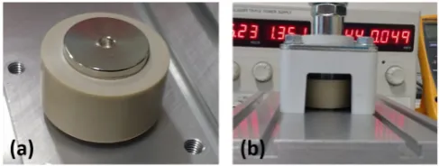
A Cree/Wolfspeed manufactured silicon carbide Schottky diode with datasheet reference CPW5-1200-Z050B was used in the module. Enclosing the diode is a polypropylene sulfide (PPS) die carrier, used for positioning the elements of the assembly as shown in Fig 1. The external clamping force was applied using a commercial clamping kit and heatsinks. The module internal interface layers are pressed by the external force exerted by the clamping kit in order to establish the appropriate electrical and thermal contact at the interfaces of the assembly. An external case made of Polyether ether Ketone (PEEK) was used for aligning the copper poles. A detailed view of the real prototype and the assembled clamp is shown in Fig 2.
Fig 2: (a) Press-pack prototype, including the external case, (b) Detail of the assembled clamp with the press-pack diode
III. FINITEELEMENTMODELLING
The finite element modelling capture direct coupling between the physics involving joule heating, thermal expansion and subsequent mechanical deformation and hence stresses on the structure. By exploiting symmetry in the module, one quarter symmetry has been assumed in this modeling study. The model of the press-pack package was developed in the finite element code ANSYS [13]. Complexity of the model structure can be further reduced by represent the effect of the heat sink as an equivalent heat transfer coefficient. This is detailed below.
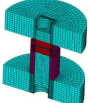
[image:3.595.307.551.358.450.2]the associated solid element (in this study, SOLID226). Coulomb and shear stress friction exists between contact and target surfaces. The volume of the structure was discretised using SOLID226 element which has electro thermo-mechanical capabilities. After undertaking a mesh sensitivity analysis a model consisting of approximately 20,000 elements was used for all investigations, as shown in Fig. 3.
Fig 3: Cross-section of the meshed model of the press-pack diode ANSYS
A. Thermal Contact Resistance
Contact interfaces are never perfectly flat due to surface roughness. Thermal contact resistance depends on the surface, material hardness, and contact pressure at the interface. Assuming that heat transfer is dominated by conduction at these interfaces, then the following equation can be used for thermal contact resistance [14]
(
)
95 . 0
2 1
2 1
5
.
2
1
+
=
H
P
m
k
k
k
k
R
Thermalσ
(1)wherek1,k2are the thermal conductivities of the contacting
materials. The parameters σ, m, P, H are respectively the
effective root mean square (RMS) of surface roughness, mean absolute slope of the interface as in Fig 4, contact pressure of the joint and hardness of the softer material. If the mean
absolute slope (m) is not available, then mean absolute asperity
slope can be approximated by the correlation equation (2)
(
6)
0.40210
125
.
0
×
=
σ
m
(2) [image:4.595.49.289.97.259.2]which is valid for an effective RMS of surface roughness (σ) range of 0.216 μm ≤ σ ≤ 9.6 μm [15]. The effective root mean square (σ) values calculated in this study are within the range of 0.216 μm to 9.6 μm. The average rms surface roughness of the molybdenum and ALG contacts was characterized obtaining 1.1 μm for the ALG contacts and 1 μm for the molybdenum contacts. The characterized surface of the ALG is shown in Fig. 5.
[image:4.595.307.543.205.458.2]Fig 4: Rough surface schematic
Fig 5: Characterization of the surface of the ALG contact
B. Electrical Contact Resistance
Electrical contact resistance also depends on the contact force and the hardness of the contacting materials. When electrical current pass through the contact interface the current lines are restricted to pass through the reduced contacting area, this will result in an increase in electrical resistance at the interface Assuming that the asperities at the SiC and pad surfaces form circular contact areas, then the following equation can be used to predict electrical contact [16, 17]
(
)
F
H
R
Elec Conπ
ρ
ρ
4
2 1 _
+
=
(3)whereρ1, ρ2, andF, are respectively electrical resistivity of
the materials 1 and 2, and applied force on the contact joint. The above equation is widely used by design engineers to estimate the contact resistance. The equation is valid over a wide range of applied loads and contact materials [17]. Other more complex models (requiring additional materials data) are also available [18]. The Vickers hardness of the Mo was chosen as TABLE I: MATERIAL PROPERTIES OF PRESS PACK MODELING
Material
Property Mo AlG2208
Cu PPS SiC
Density (Kg/m3) 10220 2300 8930 1350 3210 Poisson Ratio 0.38 x,y:0.16
z:0.2 0.343 0.3 0.14
CTE(μm/m°C) 5.35 x,y:8
z:12 16.4 49 4
Young’s
Modulus (GPa) 330 33 110 4.34 476
Thermal conductivity (W/m°C)
138 x,y:220
z:140 385 0.255 370
Specific Heat
(J/Kg/C) 217 800-950 385 - 750
Resistivity (Ω/m)
5.3e-8 x,y : 4e-7 z : 6e-7
1.6e-8
[image:4.595.125.212.355.457.2]C. Boundary condition
In the mechanical predictions the mechanical contact between contacting surfaces is controlled by friction. A friction coefficient of 0.75 was assumed between contact layers Cu/Mo (or ALG). Similarly friction coefficient of 0.5 is assumed for SiC/Mo (or ALG) interface [10]. Clamping pressure varies for single diode package, hence a quarter of the original intended pressure was applied on the one quarter model we simulated. Electric current was applied to anode/heatsink interface by coupling the finite element mesh nodes and applying the current load to the master node.
D. Single Sided Cooling
Estimating the impact of the heat sink with a suitable heat transfer co-efficient is detailed as follows. Natural free flow
convection coefficient is assigned as 10 W/m2k based on the
reference [21, page 422 (Table 9.1)]. From the heat sink manufacturer specifications, the surface area of the heatsink can be extracted. Hence the heat transfer coefficient representing
the heatsink was approximated ashHeatsinkas in equation (4).
Convection Natural Interface
Heatsink Heatsink h
A A
× =
h (4)
Where AHeatsink -the heatsink surface area exposed to the
natural free flow convection andAInterface- the model interface
area between the anode (cathode) and hNatural Convection- the
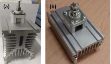
standard natural free flow convection coefficient. Two commercial heat sinks (recommended for press-pack assemblies) have been investigated: A large heatsink model PS260/150B and a small heatsink model PS136/150B, both from GD Rectifiers [22]. The rationale for using the large and small heat sinks was to investigate the impact of heatsink size of heat extraction. For the large heatsink and small heatsink the
heat transfer coefficients were approximated as 12893 W/m2k
and 4991 W/m2k respectively. The complete assembly for both
[image:5.595.315.547.202.305.2]heatsinks is shown in Fig. 6.
Fig 6: Single sided heatsink and box clamp assemblies for the press-pack prototype: (a) Large heatsink (b) Small heatsink
IV. SIMULATION ANDRESULTS
Using the developed model as detailed above, the combined
thermal contact resistances were dominated by the clamping pressure; for example, if clamping pressure increases, then the contact resistances decreases, but the stresses on the chip increases. The average von Mises stress on chip and the average temperature on the chip were extracted by volume weighted averaging method, which is widely reported in the literature. The plots of temperature and electric potential distributions of the structure are given in Fig 7.
Fig 7: For AlG contact pad, 400 N clamping force, 20 A loading and for large heatsink, (a) Temperature (°K) distribution on the structure (b) Electric potential (V) distribution on the structure.
A. Thermal Distribution on the Diode
[image:5.595.307.520.443.554.2]Fig 8 illustrates the temperature distribution on the diode chip for 400 N constant clamping force for both Mo and ALG contact pads. Clearly the use of an ALG pad is resulting in a lower temperature distribution across the diode compared with Mo pad. This trend (as in Fig 9 and Fig 10) was also observed for other clamping pressure, electrical loadings, and heat sink designs combination.
Fig 8: Temperature (°K) distributions on diode for 20 A loading, 400 N clamping force and with large heatsink (a) Model with Mo pad and (b) Model with ALG pad
By considering the temperature distribution on the diode chip as dominant factor, the model with ALG contact pad outperform the model with Mo contact pad. This observation agrees with our expectation, since the hardness value of ALG is low in comparison with the hardness value of Mo. Hence small electrical and thermal contact resistances and consequently small average temperature on the model with ALG pad. As expected, increasing the load current value increases the diode temperature distribution (as in Fig 11) for both models (ALG and Mo contact pad).
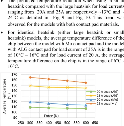
[image:5.595.82.265.531.636.2]• The predicted temperature reduction when using a small heatsink compared with the large heatsink for load currents ranging from 20A and 25A are respectively ~13°C and ~ 24°C as detailed in Fig 9 and Fig 10. This trend was observed for the models with both contact pad materials.
• For identical heatsink (either large heatsink or small
[image:6.595.44.290.90.339.2]heatsink) models, the average temperature difference of the chip between the model with Mo contact pad and the model with ALG contact pad for load current of 25A is in the range of 10°C – 16°C and for load current of 20 A, the average temperature difference on the chip is in the range of 6°C -10°C.
[image:6.595.307.531.243.349.2]Fig 9: Average temperature (°C) plot versus clamping force (N) of diode on model with small heatsink (PS136) for 20 A and 25 A loading.
Fig 10: Average temperature (°C) plot versus clamping force (N) of diode on model with large heatsink (PS260) for 20 A and 25 A loading.
Fig 11: Average temperature (°C) plot versus loading current (A) of diode on models with 300 N clamping force.
It should be noted that the predicted difference between maximum and average temperature across the diode is < 5°C in all simulations. Hence the reported temperatures are representative of the junction temperature in the diode. For silicon carbide the maximum operating junction temperature based on manufacturer’s specification should not exceed
175°C. Hence for even small heatsink the chip temperature at 25A load current is within the operating temperature regime. This can provide benefits when smaller form factor of the overall assembly is required.
B. Stress Distribution on the Diode
The von Mises stress distributions on the diode for both contact pad material models using 400N clamping force and 20A current loading is illustrated in Fig 12. Unlike the trends observed for temperature, the average von Mises stress in the diode is higher for ALG contact pad compared with Mo contact pad. This trend (as in Fig 13) was also observed for various load
currents, clamping pressures and heatsinks model
[image:6.595.46.288.367.471.2]combinations.
Fig 12: von Mises stress (N) distributions of diode for 20 A loading and 400 N clamping force and with large heatsink (a) on diode with Mo pad and (b) on diode with ALG pad
[image:6.595.307.549.493.595.2]The maximum stress on the chip observed in the FEA simulation is 190 MPa. It should be noted that the yield stress of SiC is 21 GPa [23]. According to Sharp et al [24], the fracture strength of smooth SiC of any shaped specimen is in the range of 0.5 – 1.5 GPa. Additionally in the experiment we haven’t observed any crack in the chip for both contact pad materials. Hence these predicted stresses in the diode are significantly below this value and should not be of concern in terms of mechanical failure of the diode during the assembly process.
Fig 13: Average von Mises stress (MPa) on diode plot versus clamping force (N) on models with small heatsink (PS136) for 10 A and 15 A loadings.
From the results, it can be concluded that average von Mises stress on the diode increases from large heatsink model to small heatsink model by less than or equal to 3MPa. This additional stress increment is due to percentage stress induced by thermal load increment.
90 100 110 120 130 140 150 160 170
250 300 350 400 450 500 550 600 650
Av
er
ag
e
Te
m
pa
ra
tu
re
(°
C)
Force (N)
20 A Load (AlG) 25 A Load (AlG) 20 A Load (Mo) 25 A Load(Mo)
90 100 110 120 130 140 150 160 170
250 300 350 400 450 500 550 600 650
Av
er
ag
e
Te
m
pa
ra
tu
re
(°
C)
Force (N)
20 A Load (AlG) 25 A Load (AlG) 20 A Load (Mo) 25 A Load(Mo)
50 100 150
8 11 14 17 20 23 26
Av
er
ag
e
Te
m
pe
ra
tu
re
(°
C)
Load Current (A)
Mo Pad (Small Heatsink) AlG Pad (Small Heatsink) Mo Pad (Large Heatsink) AlG Pad (Large
Heatsink) 10
20 30 40 50 60
250 300 350 400 450 500 550 600 650
Av
er
ag
e
vo
n
M
is
es
St
re
ss
(M
Pa
)
Force (N)
[image:6.595.45.290.500.602.2]In order to verify the numerical results experimental measurements of junction temperature were performed. The traditional DC power cycling setup [25] shown in Fig 14(a) has been used for the evaluation of the performance of the press-pack diode as Device Under Test (DUT), with a picture of the test setup configuration using the large heatsink assembly as DUT shown in Fig. 14(b). In this experimental configuration a DC heating current is used for increasing the temperature of the device due to self-heating and when this heating current is switched off, the forward voltage across the device at low current is used as a Temperature Sensitive Electrical Parameter (TSEP) for the estimation of the junction temperature [26]. The calibration of the TSEP was done using a thermal chamber, measuring the forward voltage at low current at different temperatures and clamping forces, leaving enough time to reach the thermal equilibrium, hence assuming that the temperature in the chamber is the temperature of the chip.
Fig 14: (a) Electrical schematic of the test circuit, .(b) Detail of the test circuit, where the auxiliary switch and the DUT can be identified.
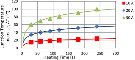
The heating tests have been performed for various combinations and the junction temperature increment from ambient temperature against time were plotted as in Fig 15 and Fig 16. The trend curves of power equation were fitted to the discrete data sets. Assuming the junction temperature stabilises after a certain amount of time then we can extract the stabilised junction temperature of the structure for a constant loading current and clamping force. The time period for stabilised temperature was assumed to be 3600 seconds for obtaining the trend curve equation of junction temperature increment.
[image:7.595.307.528.107.200.2]Comparing Figs 15 and Fig 16 it can be clearly observed how the temperature increase is smaller when ALG contacts are used. Fig 17 presents the stabilised junction temperature increase for both contact materials, using a heating current of 10 A, a clamping force of 500 N and the large heatsink model PS260. The impact of the clamping force on the junction temperature increase is presented on Fig 18. Using molybdenum as intermediate contact, the effect of the clamping force (300 N and 500 N) has been measured for two heating currents, namely 10 A and 20 A. For the SiC device used in this study, the forces of 300N and 500N are based on the recommendations from Lutz et al [27]. These recommndations state that clamping pressure should lie within the range 10
[image:7.595.309.530.232.330.2]Fig 15: Experimental results of diode temperature (°C) versus time (s) for small heatsink, on ALG pad for 300 N clamping pressure.
[image:7.595.68.280.299.393.2]Fig 16: Experimental results of diode temperature (°C) versus time (s) for small heatsink, on Mo pad for 300 N clamping pressure.
Fig 17: Experimental results of diode temperature (°C) versus time (s) for large heatsink for both contact pad models for 500N and 10A loading.
Fig 18: Experimental results of diode temperature (°C) versus time (s) for large heatsink for model with Mo pad for 300N and 500 N clamping force and 10A, 20A loading
VI. COMPARISON OFFINITE ELEMENTRESULTS WITH
EXPERIMENTALRESULTS
Since the FEA modelling does not consist of the time dependent material properties in the modelling, the FEA modelling results were compared with stabilised temperature extracted from the experiments. The clamping force has less
0 20 40 60 80 100 120
0 50 100 150 200 250 300
Ju nc tio n Te m pe ra tu re In cr ea se , Δ T (° C)
Heating Time (s)
10 A 20 A 30 A 0 20 40 60 80 100 120
0 50 100 150 200 250 300
Ju nc tio n Te m pe ra tu re In cr ea se , Δ T (° C)
Heating Time (s)
10 A 20 A 30 A 0 10 20 30 40 50 60
0 600 1200 1800 2400 3000 3600
Ju nc tio n Te m pe ra tu re In cr ea se , Δ T( °C )
Heating Time (s)
500 N - ALG 500 N - Mo
0 10 20 30 40 50 60 70 80 90
0 600 1200 1800 2400 3000 3600
Ju nc tio n Te m pe ra tu re In cr ea se , Δ T (° C)
Heating Time (s)
[image:7.595.310.537.364.455.2] [image:7.595.308.552.486.581.2]impact on the junction temperature rise than the contact material, as it can be observed in Figs 19 to 21, where a combination of test assemblies (contact material, clamping force and model of heatsink) has been evaluated to validate the model presented in this paper.
[image:8.595.48.277.285.383.2]Fig 19: Junction temperature (°C) on diode versus clamping force (N) for large heatsink, finite element and experimental results for 10 A and 20 A loading on Mo contact pad.
Fig 20: Junction temperature (°C) on diode versus clamping force (N) for large heatsink, finite element and experimental results for 10 A and 20 A loading on ALG contact pad.
These results follow the trend shown in the simulations and suggest a better thermal performance of the ALG contact. The FEA results slightly under predict the junction temperature in comparison with the experiments due to the approximated value of certain parameters in the FE modelling. Overall the experiment and finite element modelling follow the trends (1) The reduction in junction temperature for increased clamping pressure, (2) ALG contact pad model generated lower junction temperature in comparison with Mo pad model.
Fig 21: Junction temperature (°C) on diode versus clamping force (N) for small heatsink, finite element and experimental results for 10 A and 20 A loading on ALG contact pad.
The impact of the contact material and the clamping force on the thermal resistance was measured and characterized in [28] using advanced equipment. From the results presented,
increasing the force reduces the thermal resistance and the press-pack assembly with ALG contacts has also a lower thermal resistance, corresponding with the modelling results obtained in this the paper.
VII. CONCLUSION
A novel combined electro-thermo-mechanical modelling methodology for assessing diode temperature and stress imposed on the diode in the press-pack packaging process is demonstrated. Based on the assumptions made in this work, for load currents ranging from 20-25A, and clamping forces ranging from 300-500N, the results show that.
•
Both contact pad materials Molybdenum andAluminum Graphite result in junction temperatures that meet manufacturers specifications
•
Both contact pad materials result in stresses in thediode that are well below any stress that could cause mechanical failure in the diode
•
Using Aluminum Graphite results in a lower junctiontemperature compared with Molybdenum (~6-16C for process parameters investigated in this study). Hence using Aluminum Graphite could result in a significant increase in overall diode reliability.
•
Adoption of a smaller heat sink design also meetsmanufacturer specifications in terms of junction temperature. This can aid design engineer to meet smaller form factor requirements for the package.
•
Model results compare with experimental data both interms of junction temperatures and temperature trends for both contact pad materials.
Based on the methodology detailed in this paper a packaging design engineer can use any contact pad material whose thermal and mechanical properties are known. If the surface roughness of the interfaces is also known these can easily be included into the analysis to provide values of thermal and electrical contact resistances. Hence the developed methodology provides significant benefits to packaging engineers in identifying clamping forces and packaging materials that meet temperature, form factor, and reliability requirements for specific package designs and applications.
VIII. ACKNOWLEDGEMENT
This research has been funded by the Engineering and Physical Science Research Council (EPSRC) through the Underpinning Power Electronics HUB (EP/K035304/1).
REFERENCES
[1] F. Wakeman, K. Billett, R. Irons and M. Evans, Electromechanical characteristics of bondless pressure contact IGBT, 14th Annual Conference of Applied Power Electronic Conference and Exposition (APEC), Dallas, Texas, Mar 1999, pp 312 – 317
[2] M. H. Rashid, Power electronics handbook, 3rd edition, Butterworth-Heinemann, 2011
[3] J. Lutz, H. Schlangenotto, U. Scheuermann and R. D. Doncker, Semiconductor power devices: Physics, characteristics, and reliability.
0 20 40 60 80 100 120
250 300 350 400 450 500 550
Ju nc tio n Te m pe ra tu re , T (° C)
Clamping Force (N)
10 A Load, Large Heatsink (Mo FEA Simulation) 10 A Load, Large Heatsink (Mo Experiment) 20 A Load, Large Heatsink (Mo FEA Simulation) 20 A Load, Large Heatsink (Mo Experiment) 0 20 40 60 80 100 120
250 300 350 400 450 500 550
Ju nc tio n Te m pe ra tu re ,T (° C)
Clamping Force (N)
10 A Load, Large Hestsink (ALG FEA Simulation) 10 A Load, Large Heatsink (ALG Experiment) 20 A Load, Large Heatsink (ALG FEA Simulation) 20 A Load, Large Heatsink (ALG Experiment) 0 20 40 60 80 100 120
250 300 350 400 450 500 550
Ju nc tio n Te m pe ra tu re , T (° C)
Clamping Force (N)
[image:8.595.50.285.530.626.2]Electro-thermo-mechanical analysis of high – power press –pack insulated gate bipolar transistors under various mechanical clamping conditions, Institute of Electrical Engineers of Japan Journal of Industry Applications, 3(3), pp 192 – 197, 2014
[5] T. Poller, S. D’Arco, M. Hernes, A. R. Ardal, J. Lutz, Influence of the clamping pressure on the electrical, thermal and mechanical behavior of press – pack IGBTs, Microelectronics Reliability, 53, pp 1755 – 1759, 2013 [6] T. Poller, T. Basler, M. Hernes, S. D’Arco and J. Lutz, Mechanical analysis of press – pack IGBTs, Microelectronic Reliability, 52, pp 2397 – 2402, 2012
[7] A. Hasamasan, C. Busca, R. Teodorescu and L. Helle, Modelling the clamping force distribution among chips in press – pack IGBTs using the finite element method, 3rd IEEE International Symposium on Power Electronics for Distributed Generation Systems (PEDG), Aalborg, pp 788 – 793, June 2012
[8] A. Pirondi, G. Nicoletto, P. Cova, M. Pasqualetti, and M. Portesine, Thermo – mechanical finite element analysis in press – packed IGBT design, Microelectronics Reliability, 40, pp 1163, 1172, 2000
[9] A. Pirondi, G. Nicoletto, P. Cova, M. Pasqualetti, M. Portesine and P. E. Zani, Thermo-mechanical simulation of a multichip press-packed IGBT, Solid State Electronics, 42 (12), pp 2303 – 2307, 1998
[10]T. Poller, J. Lutz, S. D’Arco, and M. Hernes, Determination of thermal and electrical contact resistance in press-pack IGBTs, 15th European conference on Power Electronic and Applications, Lille, France, pp 1-9, Sep 2013
[11]C. Busca, R. Teodorescu, F. Blaabjerg, L. Helle and T. Abeyasekera, Dynamic thermal modelling and analysis of press – pack IGBTs both at component – level and chip – level, 39th IEEE Conference of Industrial Electronics Society (IECON), Vienna, pp 677 – 682, Nov 2013
[12]Hoffmann & Co Elektrokohle AG, Aluminum Graphite Composites, http:/www.hoffmann.at
[13]ANSYS® Academic Research, Release 12.0, Help System, Coupled Field Analysis Guide, ANSYS, Inc
[14]M. M. Yovanovich, Four decades of research on thermal contact, gap and joint resistance in microelectronics, IEEE Transactions on Components and packaging technologies, 28(2), 2005
[15]V. W. Antonetti, T. D. Whittle and R. E. Simons, Approximate thermal contact conductance correlation, American society of mechanical engineers, Journal of Heat Transfer, 170, pp 35 – 42, 1991
[16]S. Ganesan and M. G. Pecht, Lead – free electronics, John Wiley & sons, 2006
[17]P. G. Slade, Electrical contacts, principles and applications, 2nd edition, CRC Press, 2014
[18]M. Ciavarella, G. Murolo, and G. Demelio, The electrical/thermal conductance of rough surfaces –Weierstrass-Archard multiscale model, International journal of solids and structures, 41 (15), 2004, pp 4107 – 4120 [19]P. Sharma, S. Sharma, and D. Khanduja, A study on microstructure of aluminum matrix composites, Journal of Asian Ceramic Societies, 3, 2015, pp 240 -244
[20]M. Winter (2010), Web elements, Retrieved from http://www.webelements.com/molybdenum/physics.html
[21]J. Walker, Handbook of RF and microwave power amplifiers, Cambridge University press, 2012
[22]GD Rectifiers Ltd, http://www.gdrectifiers.co.uk/
[23]T. Kimoto, J. A. Cooper, Fundamentals of silicon carbide technology: Growth, characterization, devices, and applications, John Wiley & Sons, 2014
[24] W. N. Sharp, G. M. Beheim, L. J. Evans, N. N. Nemeth and O. M. Jadaan, Fracture strength of single crystal silicon carbide microspecimens at 24 °C and 1000 °C, Journal of microelectromechanical systems, 17 (1), 2008 [25]L. R. GopiReddy, L. M. Tolbert and B. Ozpineci, "Power Cycle Testing of
Power Switches: A Literature Survey," in IEEE Transactions on Power Electronics, vol. 30, no. 5, pp. 2465-2473, May 2015
[26]Y. Avenas, L. Dupont, and Z. Khatir, Temperature measurement of power semiconductor devices by thermos-sensitive electrical parameters – A review, IEEE Transactions on Power Electronics, 27 (6) , June 2012, pp 3081 – 3092
Springer Verlag, 2011
[28] J. Ortiz Gonzalez et Al., Development and characterisation of pressed packaging solutions for high-temperature high-reliability SiC power modules, Microelectronics Reliability, Volume 64, Sep. 2016, Pages 434-439
Pushpa Rajaguru received his MPhil and PhD degrees in computational
mathematics and Multiphysics modelling from university of Salford and University of Greenwich. Since 2011, he is a researcher in Computational Mechanics Reliability Group of University of Greenwich.
Hua Lureceived the Master’s degree in condensed matter
physics from Wuhan University, Wuhan, China, in 1988, and the Ph.D. degree in computational physics from the University of Edinburgh, Edinburgh, Scotland, in 1992. He is a Reader (Associate Professor) in computational science with the School of Computing and Mathematical Sciences, University of Greenwich, London, U.K. He has published more than 40 technical papers in journals. His current research interests include multiphysics computer modeling of electronic components, reliability prediction methods, and design and manufacturing optimization methods and applications.
Chris Baileyreceived his PhD in Computational Modelling
from Thames Polytechnic in 1988, and an MBA in Technology Management from the Open University in 1996. Before joining Greenwich in 1991, he worked for three years at Carnegie Mellon University (USA) as a research fellow in materials engineering. He is the Professor of Computational Mechanics and Reliability Group (CMRG) at the University of Greenwich, London. His research group focuses on the development of virtual prototyping tools based on Multiphysics modelling and numerical optimisation. Chris is a committee member of the International Microelectronics and Packaging Society (IMAPS) and the Innovative Electronics Manufacturing Research Centre in the UK.
Jose Angel Ortiz Gonzalezreceived the B.S. degree in
electrical engineering from the University of Vigo, Vigo, Spain, in 2009. From 2010 to 2012, he was a Support Technician with the Department of Electronics Technology, University of Vigo. Since 2013, he has been with the School of Engineering, University of Warwick, as a Power Electronics Research Assistant, while pursuing a PhD in power electronics. His research interests include reliability of power semiconductor devices and condition monitoring.
Olawiwola Alatisereceived the BEng degree (first-class