C. Klumpner
University of NottinghamSchool of Electrical and Electronic Engineering, University Park Nottingham, NG7 2RD, United Kingdom
Abstract- Renewable energy sources such as photovoltaics (PVs) or fuel cells (FCs) are not fitted for direct power grid connection because they deliver DC voltage and current. This is why a power electronic interface is needed, consisting usually of a current-mode operated step-up DC/DC converter with/without isolation that boosts the voltage at a level that can be processed by a DC/AC inverter. This paper presents the implementation of a three-phase power electronic interface for PV/FCs that uses a single conversion stage approach based on a current source inverter (CSI) topology that would need only six reverse blocking IGBTs. In order to overcome the poor switching behavior of this device, a new way of implementing the CSI is proposed, which is proved to be more efficient. A new cost-effective CSI topology for multiple DC sources independently controlled is also proposed. The performance is assessed both in simulation and experimental.
I. INTRODUCTION
In the last 200 years, fossil fuels powered primarily the world economy mainly because they are cheap as there is no other cost associated with their production, but only with their extraction and transportation. As a result, the concentration of CO2 in atmosphere raised by 50% compared to pre-industrial
levels and is expected to double by the time the reserves of fossil fuel are depleted. Among the negative effects of relying heavily on fossil fuels is not only the risk of global warming, but also a price surge of this commodity. However, there is a positive aspect here: higher oil prices makes the use of alternative renewable energy supplies more price competitive, with wind and solar energy directly converted into electricity
becoming economically feasible. This is demonstrated by the rate of which the installed power increased in the last 10 years. In order to increase the utilization of renewable energy sources such as photovoltaics (PVs) and fuel cells (FC), more research is needed to constantly decrease their specific costs ($/kW installed), one important part being not only the capturing of the renewable energy cheaply, but also interfacing it to the power grid in a cost effective way.
There are a few alternative power converter topologies available to connect a FC/PV to the AC power grid [1]-[3], as illustrated in Fig. 1. First topology shown in Fig. 1a consist of a two-stage arrangement: a DC/DC converter is used to boost the low voltage typically delivered by the FC/PV to a higher level suitable for the DC/AC inverter. As the DC/DC inverter is not galvanically isolated, it means that additional precaution when designing the DC/DC inverter should be considered in order to comply with the safety regulations and to contain any potential EMI [3]. In case the DC/DC converter provides galvanic isolation by means of a high frequency transformer as sugested in Fig. 1b, all the latter issues are automatically solved. In addition, the high frequency transformer is small and operates typically with very high efficiency (99%) and because it allows the adaptation of the semicondutcor voltage/current levels, it will require an installed power in semiconductors close to the power processed which means it will not be very expensive. The third solution illustrated in Fig. 1c consist of a
DC
DC AC DC
FC/ PV
[image:1.612.84.532.540.682.2]1/3~ Power grid
Fig. 1. Topologies of power converters for connecting PV/FC to the AC power grid: a) using a non-isolated DC/DC converter followed by a DC/AC inverter; b) using a DC/DC inverter with a high frequency transformer followed by a DC/AC inverter; c) using a DC/AC inverter
followed by a low frequency step up transformer; d) using a single stage DC/AC inverter. DC
DC FC/
PV
DC AC
1/3~ Power grid
AC DC FC/
PV
1/3~ Power grid FC/
PV
DC AC
1/3~ Power grid
(b)
(a) (c)
DC/AC inverter that converts the DC power delivered by the FC/PV into AC voltage at the supply frequency which is stepped up at the grid level by a low frequency transformer, making this solution the simplest technologically, but due to the large size of a 50/60 Hz transformer, the bulkiest/heaviest.
The last solution presented in Fig. 1d consist of a single stage DC/AC converter, which seems the simplest but has several drawbacks that are sumarized here. As the Voltage Source Inverter (VSI) is the most popular grid side interface [3]-[6], a higher voltage level than the peak line-to-line grid voltage level will be necessary on the DC-side (FC/PV) to provide proper operation. In case of a 415 Vrms line voltage, this means that the FC/PVs have to be connected in series to deliver voltage in excess of 585V, which raises serious safety issues [3]. On the other hand, an important requirement is that the current drawn from the FC/PV terminals to have a low ripple, which would require additional DC-side filtering but would make the current source inverter (CSI) [7]-[13] an ideal choice. In addition, the CSI has the capability to boost the voltage from the DC side to the AC side which means that a lower DC-voltage would be needed, solving partly the safety issues. However, this option to reduce too much the DC-side voltage is not economical as the higher the DC/AC voltage transfer ratio is, the higher the installed power in the semiconductors would be and so the cost. Actually, the smallest voltage transfer ratio a current source inverter can achieve whilst still providing sinusoidal grid currents is 1.154.
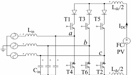
Another thing to be considered is the amount of semiconductor devices necessary to be used. A VSI would require 6 IGBTs and 6 antiparalel diodes, which is the same for a CSI built with a discrete implementation of a switch made by connecting an IGBT in series with a diode that is able to block reverse voltage. If the newly developed reverse blocking IGBT [14]-[18] is considered, there is no need for the series diode to provide blocking of reverse voltages and the situation regarding the total number of power devices becomes better for the CSI, as shown in Fig. 2. Last thing to mention is that because CSIs operate with unidirectional DC-current, it will not need a diode on the PV/FC side to prevent reverse currents.
The use of a CSI needs to be carefully evaluated against aditional restrictions such as the cancelation of the low-frequency common mode voltage dictated mostly by the way the FC/PV has its middle point pottential grounded or not and also by the high-frequency components in the common mode and differential mode generated voltages, as these will impact the size of the EMC filter that needs to be connected between the converter and the FC/PV [3]. Due to the fact that there is very little energy storage on the DC-side of the converter, the CSI will not be suitable for use in single phase systems nor power grids that operate with a large degree of unbalance.
II. ANALYSIS OF THE CURRENT SOURCE INVERTER LOSSES The switching state of the CSI can be represented by a group of two letters, that designate which of the AC lines are connected to the positive and negative DC-link terminals
respectively (“bc” means input phase b is connected to P and c
is connected to N). A zero current vector is normally produced when only two switches in the CSI leg are on, which cause a shortcircuit of the two DC-side terminals that will now be connected also to the input line that corresponds to the ON leg. An interruption in the input currents will appear, as the inductor a current freewheels through the inverter leg.
A method often used in modern PWM converter control is the Space Vector Modulation (SVM) [7]. This technique uses a combination of two adjacent vectors and a zero-vector to synthesize a reference vector of variable amplitude and angle. The proportion between the two adjacent active vectors gives the direction, and the zero-vector duty-cycle determines the magnitude of the reference vector. The input current vector Iin (Fig. 3) is the reference vector. The duty-cycles of the active switching vectors used in the rectification stage Iγ, Iδ are
calculated using (1). The duration of the zero-vector completes the switching sequence.
(
*)
sin
3
ind
γ= ⋅
m
π −θ
sin
*in
d
δ= ⋅ θ
m
d
0= − −
1
d
δd
γ (1) where m is the rectifier modulation index and θ*in the angle within the sector of the input current reference vector. These duty-cycles are multiplied with the switching period in order to determine the on-times of the switches.
The average voltage in the DC-link is calculated by knowing the duty-cycles of the two active switching states and their corresponding line-to-line voltages:
VPN-avrg = dγ⋅Vline-γ + dδ⋅Vline-δ (2)
The maximum voltage a CSI operating as a rectifier (AC/DC) can produce is revealed when replacing m=1 and θ*
in
= π/6, which will lead to dγ = dδ =0.5 and d0= 0. Because the
Iγ Iδ
Iin θ*
in dγ⋅Iγ
dδ⋅Iδ
bc ac ab
cb
ba ca
Va
Vb
Vc
Fig. 3. Generation of the reference current vector in a CSI using SVM and I/O voltage and O/I current correspondence for sector 1.
TABLE I. DCVOLTAGE AND INPUT
CURRENTS VS THE SWITCHING STATE
Sw.state γ δ 0
Ref.vector “bc” “ac” “cc”
VP= Vb Va Vc
VN= Vc Vc Vc
VPN Vbc Vac 0
Ia= 0 +Idc 0
Ib= +Idc 0 0
[image:2.612.317.565.57.187.2]Ic= -Idc -Idc 0
Fig. 2. Single-stage grid interface for FC/PV application based on a CSI using only six power semiconductors (EMC filter included in DC side).
a
b
FC/ PV IDC
P
N
c
0
T1 T3 T5
T4 T6 T2
Ldc/2
Ldc/2
Cin
Lin
Cgnd
Cdc1
[image:2.612.318.568.225.325.2]two corresponding line-to-line voltages are equal to the peak value multiplied by cos(π/6), it makes the average voltage over a switching period delivered by the rectifier to reach 0.866 of the peak line-to-line voltage.
A. Analysis of CSI Switching Losses
From Table I it results that the simplest switching pattern that can be employed is 0-γ-δ-0, which for a particular switching frequency provides the minimum number of switching states, but not the best harmonic performance. More elaborate switching patterns are possible such as double-sided symmetric and asymmetric with multiple zero current vectors that may provide much better harmonic performance.
When analyzing the generation of switching losses, the following should be taken into account. The six switches of the CSI are divided into two groups each connecting the three input lines to one DC-link pole. Switching will always take place between two switches belonging to one of these two groups and the type of losses (hard turn-on+reverse recovery or hard turn-off) should be analyzed in a similar way as it is done for a voltage source inverter leg. For example, considering the upper three switches in Fig. 2, it is noted that the current delivered by the group is always negative (Fig. 4). This means that the type of switching loss will actually be determined by the sign of the line to line voltage that is found between the two switches that would perform commutation: an outgoing switch and an incoming switch, the third switch within the group remaining off during the commutation process. For example, assuming that T1 was initially ON and that the line to line voltage Vab >0, in the moment T3 will be gated (this is normally done while the outgoing device is still on, in order to provide conduction path for the inductive DC-link current, that’s why it is also referred as “overlap commutation”), the commutation process will start immediately, because the presence of a more negative potential on the positive DC-link rail will cause the reverse bias of the internal series diode within T1, therefore a hard turn-on commutation will take place in T3 accompanied by a reverse recovery of the internal diode within T1. If the sign of the line-to-line voltage between the switches involved in commutation would have been negative (Vab<0), in the moment T3 would have been gated, nothing would have happened because the potential of the positive DC-link rail initially connected to line a would have been more negative that line b, which means that the internal series diode within T3 would have stayed reverse biased. The
commutation process would have started only after the gate signal for T1 would have been removed, forcing T1 to experience a hard turn-off process whilst T3 would turn-on naturally (no losses).
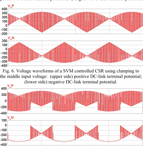
[image:3.612.320.562.241.414.2]The simplest commutation strategy is to continuously clamp one of the DC-link terminals to the highest in amplitude (positive or negative) input voltage. The potential of the input lines and of the positive and negative dc-link rails are shown in Fig. 5. At any time, the switching losses will take place in only one switch group: the three commutations that take place will always cause two hard-turn-on commutations and one turn-off or two hard turn-off commutations and one hard turn-on, but the sum of the switching voltage involved in the hard turn-on commutations will be equal to the sum of the switching voltage involved in the hard turn-off commutations and equal to the
[image:3.612.319.560.443.694.2]Fig. 5. Voltage waveforms of a SVM controlled CSR using clamping to highest in magnitude input voltage: a) Input phase-to-neutral voltages; b) positive DC-link terminal potential; c) negative DC-link terminal potential.
Fig. 7. Voltage waveforms of a SVM controlled CSR using minimum switching voltage of the negative switch group: (upper side) positive
DC-link terminal potential; (lower side) negative DC-DC-link terminal potential. Fig. 6. Voltage waveforms of a SVM controlled CSR using clamping to the middle input voltage: (upper side) positive DC-link terminal potential;
(lower side) negative DC-link terminal potential.
a
b
c
T1 T3
T5 IDC
P T1 T3
[image:3.612.59.283.607.708.2]largest momentary line-to-line input voltage. The ripple seen in each of the two DC-link rail voltages will always reveal the switching voltage which due to a constant DC current is proportional to the switching loss stress of each switch group.
Alternatively, clamping of the DC-link terminals to the middle input voltage during a zero current vector is possible (Fig. 6), which compared to the previous switching pattern, would provide reduced common mode voltage generation. Now both switch groups are experiencing switching losses during each switching period but they are not higher because the sum of the switching voltage per each group is smaller, overall remaining the same.
B. The Proposed CSI with Mixed RB devices
A third way of performing the switching is possible, as proposed in Fig. 7. Here it is chosen to minimize the switching voltage seen by one of the switch groups (in this situation the negative switch group), while most of the switching voltage stress is handled by the positive switch group. Even though overall, the sum of the switching voltage remains the same, it is possible to obtain a reduction of losses by choosing different type of switches in each group: as the RB-IGBTs have a much poorer switching behavior than a discrete IGBT+ diode, they can be used in the negative switch group, whilst the discrete IGBT+D will be used in the positive switch group. The proposed topology is shown in Fig. 8.
Even though the conduction losses will increase compared to the situation of an all RB-IGBT CSI, their level will be smaller that in an all discrete IGBT+D CSI, while most of the switching losses will be smaller than in an all RB-IGBT CSI and only slightly higher than in an all discrete IGBT+D CSI.
C. Cost-Effective Multi-DC-port CSI with Mixed RB devices
The asymmetry between the control of the two switch groups in order to minimize the conduction (using RB-IGBTs) and switching (using discrete devices) losses leads to a further development. It is possible to extend the topology proposed in Fig. 8 to a power electronic interface that connects multiple [19] renewable energy DC sources independently controlled to the same power grid, that will need only three IGBTs and three diodes per each independently controlled DC-source that is added. The negative terminals of all the DC-sources have to be connected together to the negative DC-link terminal provided by the common switch group; its switches have to be rated to the sum of the currents delivered by all the DC supplies.
III. EVALUATION OF THE CSIPERFORMANCE
Because only the datasheets of a 40A/1200V RB-IGBT manufactured by IXYS [18] was publicly available at the time this paper was finalized, it was chosen to do the comparison of the installed power in devices and the estimation of the power losses between a three-phase CSI and a VSI considering a power level processed by the CSI according to the RB-IGBT nominal ratings, despite the fact that perhaps this power level
may seem a bit inappropriate for a PV application. A pair of IGBT and fast recovery diode was chosen in order for a VSI to process the same amount of power as the CSI whilst connected to the same level of AC supply voltage.
A. CSI vs. VSI Semiconductor Installed Power
In order to evaluate the losses and the power installed in the semiconductor devices, the following assumptions have been made: a string of series connected PV/FCs is used in order to provide a high enough voltage to fully utilize the semiconductors at full load, while still being able to maintain operation near no-load condition. The specs of a BP 275 solar PV panel manufactured by BP SolarTM were used. It delivers a
no-load voltage of 21.4V and a full load voltage of 17.0 V and has a no-load vs. maximum power point voltage ratio of 1.26. The no-load voltage of the PV string connected into the CSI DC-link should allow operation at full modulation index (1/0.866), which for a 415Vrms/50Hz power supply gives a no-load voltage of 508.6 V and a maximum power point voltage of 404.0 V. For a VSI, the risk for overmodulation appears at full load, which means that the maximum power point voltage has to be at least 586.9 V (compensation for device voltage drop and for the need to limit the maximum modulation index at values below one are not included) which means that the no-load voltage will rise up to 738.8 V.
[image:4.612.328.547.53.178.2]Because of the voltage mismatch, in order to process the same amount of solar power, a higher current capability will be required for the CSI RB-IGBTs compared to the VSI IGBTs. As only the parameters of a single size RB-IGBTs are public
Fig. 8. Topology of a single-stage grid interface for FC/PV based on a CSI with asymmetric group switches using 3 RB-IGBTs, 3 normal
IGBTs and 3 fast recovery diodes with optimized losses.
a
b
FC/PV IDC
c
T1 T3 T5
T4 T6 T2 Ldc/2
Ldc/2
Lin
[image:4.612.312.565.215.341.2]Cin
Fig. 9. Cost-effective topology of a single-stage grid interface for multiple FC/PVs based on a CSI that has a common RB-IGBT lower switch group.
Ldc-N
Cin
Lin
PVn
PV2
domain (40A/1200V), a power rating that will fully load this device will be used in the simulations, which means that an equivalent current rating for the VSI IGBTs has to be found. The stress of the CSI is represented by the DC-link current (that is constant) which in this circuit is commutated by the RB-IGBTs between different input lines. This means that the rated power of a CSI using RB-IGBTs will be given by
PCSI = Pdc@full power = Vdc*Idc=404*40=16.16 kW (3)
The current rating for the VSI devices to process the same DC-link power is given by the peak value of the grid currents:
PVSI = PCSI = 3415*Ipk/ 2⇒ Ipk = 31.8 A (4)
The installed power in semiconductor devices is given by the product between the number of semiconductor devices, the maximum voltage a device is required to block and the maximum current a device has to conduct. For a CSI, the maximum voltage a device is required to block is given by the peak value of the line-to-line grid voltage (586.9 V) whilst for a VSI, this is the no-load DC-link voltage (738.8 V). For the CSI, the maximum current a device has to conduct is 40 A and for a VSI is 31.8 A. The two installed power in devices are:
Pinst_CSI = 140.86 kVA Pinst_VSI = 140.96 kVA (5)
This virtually leads to a similar power installed in the active semiconductor devices. The advantage on the CSI side is clearer if it is taken into account the fact that the CSI that would use RB-IGBTs will not need any additional diodes compared to the VSI that needs six diodes in antiparallel with each IGBT. However, it is true that because the power flow is mostly from DC to AC, these diodes can be rated at a much lower rated current because they are subject to much smaller current stress. It should also be mentioned that the CSI, by the way it operates (unidirectional DC-link current), prevents reverse currents and therefore will not need the antiseries diode that are normally supplied with the PV panel by the manufacturer, which will not only reduce cost but will also remove a source of power losses.
B. Simulation Results
A simulation model of the current source inverter controlled by using SVM was implanted in PSIM in order to evaluate the performance on both sides, the power grid and the load. The parameters of the circuit for all the simulation results are presented in Appendix A.
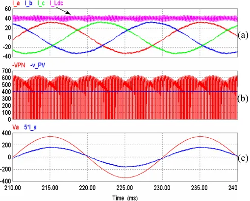
Fig. 10 shows the simulation results of the CSI operating in steady state conditions. The supply currents are balanced and sinusoidal, as revealed in Fig. 10a, and in phase with the corresponding phase voltage (Fig. 10c). The DC-link current is controlled by using a PI controller that compares the measured current with the reference, in case of a difference, its output will change the CSI modulation index. Fig. 11 shows the operation of a CSI with a topology similar to Fig. 9 but having only two independently DC-sources. The DC-terminal of the common low-side group switches has to produce a non-constant voltage (Fig. 11c) in order to keep the switching
losses low and this has to be compensated by the voltage produced by each of the DC-terminal of the upper group switches (Fig. 11a-b) in order to keep the potential difference (P-N) smooth (Fig. 11d). The capability to independently control the DC-sources is revealed in Fig. 11d where the voltage of one of the DC-sources is ramped up and in Fig. 11a where the offset in the filtered DC-terminal voltage of its corresponding upper group switch, changes (it goes negative because operates as an inverter).
C. Estimation of the Power Loss Distribution
A semiconductor loss model [20]-[23] that runs in parallel with the electrical circuit model and uses the voltages, currents (a)
(b)
[image:5.612.315.570.55.260.2](c)
Fig. 10. Simulation results of the current source inverter operating with VPV=404V and Idc_ref = 40A: a) The three input currents and the dc-link current; b) the dc-link voltage on both sides of the dc-link inductance; c) the
input phase-to-neutral voltage and corresponding current (magnified 5x).
(d) (b) (a)
[image:5.612.312.569.295.497.2](c)
Fig. 11. Simulation results of a current source inverter with two DC-sources independently controlled (one supply experiencing a voltage ramp-up): a)- b)
the instantaneous and low-pass filtered voltage of the DC-terminals of the two upper switch groups; c) the low-pass filtered voltage between each of the
and gate signals of the main simulation model of the current source inverter was also implemented in PSIM in order to evaluate the power losses in the semiconductors in three situations: when using only RB-IGBTs in the CSI; when using only a discrete implementation for the reverse blocking switching devices and when each of the two switch groups uses a different switch implementation. The parameters of the semiconductor devices are given in Appendix B. The distribution of the semiconductor losses is presented in Table II. The evaluation has been done considering the same operating conditions given in Appendix A that result in a DC-power level of 16kW injected by the CSI into the AC grid.
TABLE II. POWER LOSS DISTRIBUTION IN CSI WITH DISCRETEvs. RB-IGBTS
The first two implementations experience a very similar level of losses (<5% difference), which means that the point where the curves of the semiconductor losses versus the switching frequency intersect (11.63 kHz) is only slightly higher than the chosen switching frequency. Even though the level of the total losses is similar for the two implementations of the CSI, it should be noted that the loss estimation for the discrete implementation of the reverse blocking device use the device parameters of the IXYS MWI25-12E7 power module which include devices with a more advanced technology which have much lower specific switching losses than the IGBT that was the initial device used to develop the IXYS RB-IGBT. It is expected that a more optimised RB-IGBTs will provide lower specific switching losses as suggested in [16] where RB-IGBTs devices developed by a Fuji were reported, but the datasheets of these devices are not public domain yet.
A big difference in the level of losses is noted in the third situation with the total losses being smaller with more than 10%, which means that in term of efficiency, the mixed group switch approach is able to inherent mostly the advantages of the two standard approaches whilst minimizing its shortcomings. This approach will remain the most efficient in the switching frequency range of 6.6-47.4 kHz.
D. Experimental Results
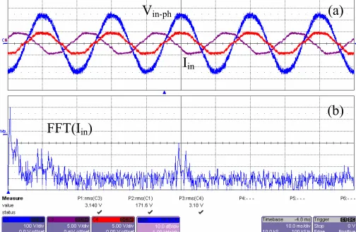
A laboratory prototype of a current source inverter (CSI) using six reverse blocking IGBTs has been developed. It uses six RB-IGBTs developed by IXYS [18] switching at 5 kHz (singlesided). The input filter consists of three 2.4 mH iron core inductors and three 6.9 µF (star connected) per each phase. The DC-link inductor has 10 mH. Only experimental results with the CSI operating in rectification mode are included.
Fig. 11 shows the grid side operation of the CSI operating as a rectifier at steady state, delivering an average voltage into the DC-link of 275 V and an average load current of 5 A, resulting in a power processed of approx 1.4 kW. The input phase voltage as seen across an input filter capacitor and two of the
grid currents reveal that the current is almost in phase with the voltage but slightly leading due to the contribution of the input filter capacitors. The FFT of the input current shows only a very small harmonics content. Fig. 12 shows the DC-side performance of the CSI in almost the same operating conditions. The DC-current ripple is approx 2A peak-to-peak
Losses CSI-RB-IGBT CSI-discrete sw
Conduction 231.6 W 1.44 % 386.1 W 2.41 % Switching 208.7 W 1.30 % 75.8 W 0.47 % Total 440.4 W 2.74% 461.9 W 2.88%
[image:6.612.314.566.131.295.2]CSI-mixed RB sw. 308.8 W 1.93 % 92.1 W 0.58 % 400.9 W 2.51%
Fig. 11. Grid side experimental result of a current source inverter operating in rectifier mode: a) the phase to neutral grid voltage as seen across an input filter capacitor (100V/div; 10ms/div) and two of the input currents (5A/div)
and b) the FFT of the input current (10dB/div; 1kHz/div). (IL= 5A).
Vin-ph
Iin
FFT(Iin)
(a)
[image:6.612.47.298.222.264.2](b)
Fig. 12. DC-side experimental result of the current source inverter operating in rectifier mode: a) The inductor current (2 A/div; 2 ms/div); the potential of the b) upper and c) the lower DC-link terminals (200V/div). (IL = 5.1A).
IL (a)
(b)
(c) Vdc_P
[image:6.612.311.565.337.495.2]Vdc_N
Fig. 13. Transient experimental results of the current source inverter operating in rectifier mode. Upper side: the inductor current (2 A/div, 100
[image:6.612.316.565.530.684.2]with a mean value of 5.1 A. The difference in the switching stress of the switches in the two switch groups is revealed by the switching voltage ripple of the upper (highly stressed) and lower (very little stressed) DC-link terminals. Fig. 13 shows a transient response of the CSI when its modulation index is changed periodically from 0.36 to 0.72. A quick and sharp response in the load current is obtained, proving that the CSI is ideal for interfacing DC-voltage sources that have their voltage highly dependent on the current they supply with the AC grid.
IV. CONCLUSIONS
In this paper, it has been shown that the utilization of the reverse blocking IGBTs can be beneficial in terms of semiconductor component count, power losses and overall performance in the interface of renewable energy sources such as photovoltaic and fuel cells with the power grid when using a well established power converter topology: the current source inverter. A new approach of implementing a current source inverter by mixing the RB-IGBT and its discrete implemented counterpart was proposed and it was proved that by adopting a clever switching pattern, an important gain in efficiency is obtained. A new cost-effective topology based on the CSI is proposed to interface multiple DC-sources to the AC grid at the cost of only 3 IGBTs and 3 Diodes each. These ideas have been demonstrated in simulations and experimentally.
V. ACKNOWLEDGMENT
Support for this work from the EPSRC is gratefully acknowledged (Grant EP/C52652X/1).
VI. APPENDIX A
Parameters for the simulation model: Vin-line= 415VRMS; fin=
50 Hz; Lin=0.5 mH; Cin=20 µF/phase; LDC = 2x0.5 mH; fsw =
10 kHz; VPV=404V; Idcref = 40A; The switching pattern is
similar to the one defined in Fig. 3: 0-δ-γ-0.
VII. APPENDIX B
Parameters used in the power loss calculations
RB-IGBT: type IXRH40N120 (IXYS); ratings: 1200V/55A@25C/35A@90C; Conduction: VCE-0=1.414V; rd-IGBT=
35.2 mΩ; Switching: tON+RR=2.54 µs; tOFF = 100ns.
Discrete IGBT+Diode: type MWI25-12E7 with NPT3 IGBT/
HiPerFREDTM (IXYS); ratings: 1200V/52A
@25C/36A@80C;
Conduction: VCE-0=1.15V; rd-IGBT=38.1mΩ; VAK-0=1.12V;
rd-IGBT=29.4mΩ; Switching: tON+RR=703ns; tOFF= 270ns.
Definition of turn-on/off loss times:
(
)
{
}
2 on RR
ON RR
CE C datasheet
E E t V I + ⋅ + = ⋅
{
}
2 off offCE C datasheet
E t V I ⋅ = ⋅ The conduction losses are modeled using:
[
0]
0
1Tsim( )
cond IGBT CE d IGBT C C sim
P V r I I dt
T
− =
∫
−+ − ⋅ ⋅ ⋅
[
]
0 0
1 Tsim( )
cond FRD AK d FRD K K sim
P V r I I dt
T
− =
∫
−+ − ⋅ ⋅ ⋅The switching losses are modeled using:
0 1 2
sim T
sw on CE on C on on t
sim
P V I t
T − − − = = ⋅ ⋅ ⋅
∑
0 1 2 sim Tsw off CE off C off off t
sim
P V I t
T − − − = = ⋅ ⋅ ⋅
∑
REFERENCES[1] G.K. Andersen, C. Klumpner, S. B. Kjær, F. Blaabjerg, "A new power converter for fuel cells with high system efficiency", Int. Journal of Electronics, Vol. 90, No. 11-12, pp. 737-750, ISSN 1362-3060, Taylor & Francis, 2003.
[2] M. Meinhardt, P. Mutschler, “Inverters without transformer in grid connected photovoltaic applications,” in Proc. of 6th European Conf. on Power Electronics and Applic. EPE’95, Vol. 3, pp. 3086–3091, 1995. [3] O. López, R. Teodorescu, F. Freijedo, J. Doval-Gandoy, “Leakage
current evaluation of a single-phase transformerless PV inverter connected to the grid”, IEEE Proc. of APEC’07, pp. 907-912, 2007. [4] I.-G. Park, S.-Y. Park, J.-K. Park, “An analysis of boost rectifier”, Proc.
of IECON’91, Vol.1, pp. 519 -524, 1991
[5] F. Blaabjerg, J.K. Pedersen, “An integrated high power factor three-phase AC-DC-AC converter for AC-machines implemented in one microcontroller”, IEEE Proc. of PESC '93, pp. 285 –292, 1993.
[6] S. Hansen, M. Malinowski, F. Blaabjerg, and M. P. Kazmierkowski, “Sensorless control strategies for PWM rectifier,” IEEE Proc. APEC’00, pp. 832-838, 2000.
[7] S. Fukuda, H. Hasegawa, “Current source rectifier/inverter system with sinusoidal currents”, IEEE Proc. of IAS’88, Vol. 1, pp. 909-914, 1988. [8] D.G. Holmes, T.A. Lipo, “Implementation of a controlled rectifier using
AC-AC matrix converter theory”, IEEE Proc. of PESC’89, pp. 353-359, 1989.
[9] N.R. Zargari, G.Joos, P.D. Ziogas, “A performance comparison of PWM rectifiers and synchronous link converters”, Proc. of International Conf. on Power Electronics and Motion Control, Vol. 1, pp. 346-351, 1992. [10] P.N. Enjeti, S.A. Choudhury, “A new control strategy to improve the
performance of a PWM AC to DC converter under unbalanced operating conditions”, IEEE Trans.on Power Electr, Vol.8, No. 4, pp.493-500, 1993. [11] T.C. Green, M. H Taha, N.A. Rahim, B.W. Williams, “Three-phase
step-down reversible AC-DC power converter”, IEEE Trans. on Power Electronics, Vol. 12, No. 2, pp. 319-324, 1997.
[12] M. Baumann, J.W. Kolar, “Analysis of the effects of nonidealities of power components and mains voltage unbalance on the operating behavior of a three-phase/switch buck-type unity power factor PWM rectifier”, IEEE Proc. of PESC’02, Vol. 4, pp. 1607 –1612, 2002. [13] C. Klumpner, J.A. Aziz, J. Clare, “A new buck-type active front end
topology with improved voltage transfer ratio and common mode voltage cancellation”, IEEE Proc. of IAS’05, Vol. 1, pp. 631-638, 2005. [14] S. Bernet, T. Matsuo, T.A. Lipo, “A matrix converter using reverse
blocking NPN-IGBT’s and optimized pulse patterns”, IEEE Proc. of PESC’96, vol. 1, pp. 107-113, 1996.
[15] A. Lindemann, “A new reverse blocking capability”, Proc. of European Conf. on Power Electronics and Applic. EPE’01, PP00389, 2001. [16] M. Takei, Y. Harada, K. Ueno, “600V-IGBT with reverse blocking
capability”, Proc. of 2001 Symposium on Power Semiconductor Devices and ICs, Osaka, paper 11.1, pp. 413-416, 2001.
[17] C. Klumpner, F. Blaabjerg, “Using reverse blocking IGBTs in power converters”, IEEE Trans. on Industry Application, IEEE Trans. on Industry Applications, Vol. 42, No. 3, pp. 807-816, May/June 2006. [18] IXRH40N120 datasheet: http://ixdev.ixys.com/DataSheet/L601.pdf
[19] C. Klumpner, F. Blaabjerg, “A new generalized two-stage direct power conversion topology to independently supply multiple AC loads from multiple power grids with adjustable power loading”, IEEE Proc. of PESC’04, paper #10249 on conf. CD-ROM, 2004.
[20] M. Bland, P. Wheeler, J. Clare, L. Empringham, “Comparison of calculated and measured losses in direct AC-AC converters”, IEEE Proc. of PESC’01, Vol. 2, pp. 1096-1101, 2001.
[21] S. Bernet, S. Ponnaluri, R. Teichmann, “Design and loss comparison of matrix converters and voltage-source converters for AC drives“, IEEE Trans. on Industrial Electronics, Vol. 49, No. 2, pp. 304-314, 2002. [22] F. Blaabjerg, J.K. Pedersen, U. Jaeger, “Evaluation of modern
IGBT-modules for hard-switched AC/DC/AC converters”, IEEE Proc. of IAS’95, Vol.2, pp. 997-1005, 1995.