The influence of ZnS crystallinity on all-electroplated
ZnS/CdS/CdTe graded bandgap device properties
OJO, A.A., SALIM, H.I. and DHARMADASA, I <http://orcid.org/0000-0001-7988-669X>
Available from Sheffield Hallam University Research Archive (SHURA) at: http://shura.shu.ac.uk/21662/
This document is the author deposited version. You are advised to consult the publisher's version if you wish to cite from it.
Published version
OJO, A.A., SALIM, H.I. and DHARMADASA, I (2018). The influence of ZnS
crystallinity on all-electroplated ZnS/CdS/CdTe graded bandgap device properties. Journal of Materials Science: Materials in Electronics, 1-18.
Copyright and re-use policy
See http://shura.shu.ac.uk/information.html
1
The Influence of ZnS Crystallinity on all-electroplated ZnS/CdS/CdTe Graded Bandgap Device Properties
A. A. Ojo*1, H.I. Salim1 2 and I. M. Dharmadasa1
1Electronic Materials and Sensors Group, Materials and Engineering Research Institute (MERI),
Sheffield Hallam University, Sheffield S1 1WB, UK.
2Department of Physics, Faculty of Science, University of Zakho, Zakho, Kurdistan-Iraq.
*Email: [email protected]; Tel: +44 114 225 6910 Fax: +44 114 225 6930
Abstract
Electrodeposition of zinc sulphide (ZnS) was achieved from electrolytic bath containing zinc
sulphate monohydrate (ZnSO4·H2O) and ammonium thiosulphate ((NH4)2S2O3) in a
two-electrode electroplating configuration. The cyclic voltammetric studies show that ZnS layers can be electroplated between (1350 and 1550) mV. The grown layers were characteristically explored for their structural, optical, morphological and electronic properties using X-ray diffraction (XRD) and Raman spectroscopy, UV–Visible spectrophotometry, scanning electron microscopy (SEM), photoelectrochemical (PEC) cell and DC conductivity measurements respectively. The structural analysis shows that crystalline ZnS can be deposited within a narrow cathodic deposition range between (1420 and 1430) mV. The UV– Visible spectrophotometry shows that the bandgap of both as-deposited and heat-treated ZnS films are in the range of ~(3.70 and 3.90) eV. The SEM shows small grains depicting the wetting property of ZnS. The PEC results show that the electroplated ZnS below 1425 mV is p-type and above 1425 mV is n-type under both as-deposited and heat treated condition. The
DC conductivity shows that the highest resistivity is at the inversion growth voltage (Vi) for
the ZnS layers. The glass/FTO/n-ZnS/n-CdS/n-CdTe/Au devices were fabricated using crystalline-ZnS and amorphous-ZnS buffer layers. The devices were explored using current-voltage (I-V) and capacitance-current-voltage (C-V) techniques. As expected, devices fabricated with c-ZnS show improved device parameters (ideality factor n=1.60, depletion width W=1092
nm, open-circuit voltage Voc=730 mV, short-circuit current density Jsc=34.1 mAcm-2, fill
factor FF=0.57, conversion efficiency η=14.2%) when compared to device parameters
(n=1.85, W=900 nm, Voc=720 mV, Jsc=29.9 mAcm-2, FF=0.52, η=11.2%) of these devices
fabricated with a-ZnS buffer layers.
2
1 Introduction
Zinc Sulphide (ZnS) from the II-VI group has been well explored for its physical, chemical and electronic properties. The optoelectronic and photovoltaic properties of this material are continually drawing more attention based on its extensive applications in light emitting diodes (LED), sensors and as buffer/window layers in photovoltaic solar cells [1,2]. The use of cadmium sulphide (CdS) as a window layer in cadmium telluride (CdTe)-based solar cells has yielded high photovoltaic conversion efficiency [3,4]. The use of CdS is constrained due to the parasitic absorption of CdS below 520 nm photon wavelengths [5] as a result of its 2.42 eV bandgap. ZnS, on the other hand, possesses a wider bandgap of ~3.7 eV [6] and has been explored as a substitute for CdS [7] but factors such as high lattice mismatch between ZnS and CdTe, the comparatively high conduction band edge of ZnS as compared to CdTe and the high resistivity of ZnS has necessitated the retention of CdS in the ZnS/CdS/CdTe solar cell configuration. Therefore, the inclusion of ZnS provides good wetting property, bandgap grading and allows for the reduction of CdS thickness without an increasing shunt [8] and reducing the parasitic absorption of CdS [5]. The buffer layer, ZnS also provides a better substrate for growing high quality CdS layer.
Several techniques have been recorded in the literature for possible growth of ZnS [9]. However, electrodeposition technique edges others with attributes such as low-cost, simplicity, scalability and the manufacturability of large area solar panels [10]. Literature records that the electrodeposition of crystalline ZnS has been achieved mainly by the
inclusion of complexing agents such as ammonia (NH3) [9], hydrazine (N2H4) [11], trisodium
citrate (Na3C6H5O7) in the electrolytic bath [12] and glycerol (C3H8O3) [13]. The literature on
the electrodeposition of ZnS without a complexing agent has been scarce and the reported ZnS layers were structurally amorphous [14,15]. With a view of cost reduction and process simplification, this paper presents in full, the electrodeposition process and characterisation of crystalline ZnS grown without the use of binding/complexing agent in a 2-electrode electrodeposition bath.
2 Experimental details
2.1 Electrolyte and Substrate Preparations
ZnS thin films were electrodeposited cathodically on glass/FTO substrates by potentiostatic technique in which the counter electrode was a high purity graphite rod. Zinc sulphate
3 98% purity were used as zinc and sulphur precursors respectively. The electrolytic bath was
prepared by dissolving 0.2 M ZnSO4·H2O and 0.2 M (NH4)2S2O3 in 400 ml de-ionised (DI)
water housed in a polypropylene beaker with a capacity of 500 ml. The polypropylene beaker was placed in an 800 ml glass beaker containing DI water. The DI water contained in the outer glass beaker helps to maintain uniform heating of the electrolyte. The solution was continuously stirred and electro-purified at 1000 mV for ~100 hours to reduce the level of impurity and also to achieve homogeneity of the solution. Afterwards, ZnS layers electrodeposited at different cathodic voltages were characterised. For these set of experiments, the bath temperature was maintained at 30˚C and the pH value of the bath was
set to 4.00±0.02 using dilute H2SO4 and NH4OH at the start of deposition. It should be noted
that the pH of the electrolytic bath should be maintained within the range of 3.00 and 4.50 due to the formation of white precipitates of sulphur and rapid deposition of ZnS layer with low adhesion to the underlying glass/FTO layer observed.
In this study, two-electrode electrodeposition configuration was utilised for simplicity. Glass/FTO and high purity carbon electrode serve as the working (cathode) and counter electrodes (anode) respectively. The working electrode of sheet resistance ~7 Ω/sq (TEC7)
was cut into 3×2 cm2 and cleaned ultrasonically before deposition. The electrodeposition
process was performed using Computerized Gill AC potentiostat. Prior to the deposition of ZnS layers, the cyclic voltammograms of the electrolyte was performed to determine the possible deposition voltage range of ZnS.
4
2.2 Material Characterisation
Data on the structural parameters of the ZnS samples such as the phase identification, preferred orientation and estimated crystallite size were acquired using Philips PW 3,710 X'pert diffractometer with Cu-Kα monochromator with a wavelength of 1.54 Å. The X-ray generator pressure and current were accordingly set to 40 kV and 40 mA. Other structural parameters such as the molecular vibration phases of the materials were extracted using Renishaw’s Raman spectrometer with an argon laser and an excitation wavelength of 514 nm. The optical properties of the ZnS layers were studied at room temperature within the wavelength range of (200 to 1000) nm using Cary 50 Scan Ultraviolet-Visible (UV–Vis) spectrophotometer. Information on the surface morphology properties of the electroplated ZnS layers was obtained using FEI Nova 200 NanoSEM at a magnification of ×60,000. The conduction type of the grown ZnS layers was determined using photoelectrochemical (PEC) cell measurement. The PEC measurement was achieved by inserting the glass/FTO/ZnS
layers into an aqueous solution comprising of 0.1 M sodium thiosulphate (Na2S2O3) to form a
solid/liquid junction. The PEC cell undergoes measurements under both illuminated and dark conditions for constant time duration. The magnitude of the difference between the measured
voltages of the PEC cell under illuminated (VL) and dark (VD) shows the suitability of doping
density of the semiconducting layer for fabricating electronic devices [16] and the mathematical sign indicates the electrical conduction type of the layer under investigation. The direct current (DC) conductivity measurement was performed to determine the electrical conductivity of the ZnS layers using fully automated Rera Solution I–V measurement system at room temperature.
2.3 Fabrication of all-electroplated ZnS/CdS/CdTe graded bandgap configuration
The effect of the crystalline property of the ZnS layers on glass/FTO/n-ZnS/n-CdS/n-CdTe/Au graded bandgap photovoltaic device as shown in Figure 1 was evaluated using both current-voltage (I-V) and capacitance-voltage (C-V) techniques. Two sets of
glass/FTO/n-ZnS/n-CdS/n-CdTe/Au devices were fabricated incorporating crystalline n-ZnS layers grown
5 Cadmium sulphide (CdS) layers with a thickness of ~65 nm were electroplated at 1200 mV on the glass/FTO/n-ZnS layer from an aqueous electrolyte. The CdS electrolytic bath
contained 0.3M cadmium chloride hydrate (CdCl2·xH2O) with a purity of 99.99% and 0.03M
ammonium thiosulphate ((NH4)2S2O3) with 98% purity in 400 ml of DI water. The bath
conditions such as the temperature and the stirring rate were maintained at 85°C and ~300 rpm respectively, while the pH was set to 2.50±0.02. The resulting glass/FTO/n-ZnS/n-CdS
layers were CdCl2 treated and annealed at 400 °C for 20 minutes in the air. Afterwards, the
layers were air-cooled and rinsed before the deposition of the n-CdTe layer.
The cadmium telluride electrolytic bath utilised for the deposition of ~1150 nm thick n-CdTe layers on the glass/FTO/n-ZnS/n-CdS contained 1.5M cadmium nitrate tetrahydrate
(Cd(NO3)2·4H2O) of 99.0% purity and 0.0002 M tellurium dioxide (TeO2) in 400 ml of DI
water. The electrolytic bath temperature, pH and the stirring rate were maintained at 85°C, 2.00±0.02 and ~300 rpm. The cathodic voltage for the deposition of the n-CdTe layers was maintained at 1400 mV. The resulting glass/FTO/n-ZnS/n-CdS/n-CdTe layers were
CdCl2+Ga2(SO4)3 treated and annealed at ~430 °C for 20 minutes in the air [17,18].
Afterwards, the layers were air-cooled, rinsed and dried in a stream of nitrogen gas. The full details of the growth and characterisation of both the CdS and CdTe layers are reported by authors’ group in the literature [19,20].
6 Before the metallisation process, the glass/FTO/n-ZnS/n-CdS/n-CdTe layers were etched using both acid and alkaline-based solutions in quick successions to improve the metal/semiconductor contact [21]. The acid etchant is an aqueous solution containing
K2Cr2O7 and diluted H2SO4, while the alkaline etchant is an aqueous solution containing
NaOH and Na2S2O3. The etching was performed by dipping the
glass/FTO/n-ZnS/n-CdS/n-CdTe layers into the acid etchant for 2 seconds, rinse in deionised water and dipped into the alkaline etchant (maintained at 60 °C) for 120 seconds. The glass/FTO/n-ZnS/n-CdS/n-CdTe layers were rinsed in deionised water afterwards, dried in a stream of nitrogen gas. The layers were transferred directly into a high vacuum metallisation system (Edward Auto 306) to deposit 100 nm thick Au contacts of 2 mm diameter on the glass/FTO/n-ZnS/n-CdS/n-CdTe layers.
3 Results and Discussions
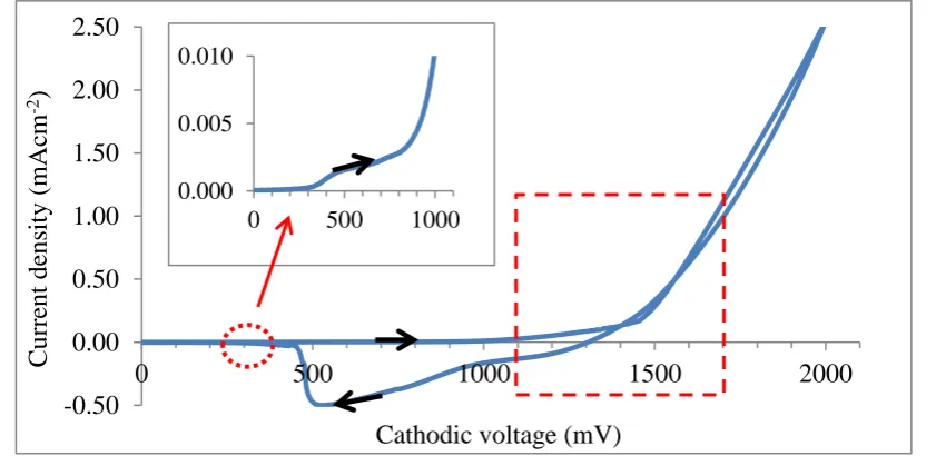
[image:7.595.84.505.479.684.2]3.1 Cyclic Voltammetry
Figure 2 shows a typical cyclic voltammogram of an aqueous solution of 0.2 M ZnSO4·H2O
and 0.2 M (NH4)2S2O3 in 400 ml of DI water during the forward and reverse cycle between
the cathodic voltages 0 and 2000 mV. The scanning rate was fixed at 3 mVs-1 with the bath
temperature, stirring rate and pH set to 30˚C, 300 rpm and 4.00±0.02 respectively.
Figure 2: Cyclic voltammogram for the electrolyte containing 0.2 M ZnSO4·H2O and 0.2 M
(NH4)2S2O3 in 400 ml of DI water at ~30˚C and pH 4.00±0.02. The inset is the expanded
forward cycle between (0 and 1100) mV. -0.50
0.00 0.50 1.00 1.50 2.00 2.50
0 500 1000 1500 2000
C
urr
ent density
(mA
cm
-2)
Cathodic voltage (mV)
0.000 0.005 0.010
7 The growth temperature was set to 30˚C to avoid vigorous sulphur precipitation which occurs at a higher temperatures and amorphous ZnS deposition which occurs at a lower temperature.
Based on the standard reduction potential values of both Zn2+ and S2- with E˚=-0.762 V and
E˚=0.449 V respectively with respect to standard H2 electrode, sulphur deposits first at ~300
mV, followed by the deposition of zinc at ~1100 mV in the forward cycle. On the reverse cycle, the dissolution of zinc starts at ~1300 mV, followed by sulphur at ~540 mV. It was deduced that between the cathodic voltage range of (1100 and 1700) mV, ZnS can be achieved as either S-rich, stoichiometric or Zn-rich ZnS. The fairly stable current density of
~1.50 mAcm-2 is observable between (1320 and 1500) mV cathodic voltages. ZnS layers
were grown within this range at the step of 50 mV and characterised to identify the approximate growth voltage in which stoichiometric/near stoichiometric ZnS can be achieved. On this initial experimentation using only XRD analysis, crystalline ZnS was observed only at 1420 mV. Therefore, surrounding cathodic potentials were explored at the steps of 10 mV to identify the optimum growth voltage. The final electrochemical equation for the formation of ZnS at the cathode can be written as equation (1).
ZnS S
e
Zn2 2 (1)
3.2 Structural Analysis
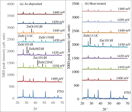
A typical XRD analysis for both as-deposited and heat treated ZnS at 300˚C for 10 minutes is shown in Figure 3 (a) and Figure 3 (b) respectively. As observed in Figure 3 (a), ZnS layers grown at cathodic voltages outside the range of 1410 to 1430 mV show an amorphous behaviour which might be as a result of the growth technique, the cathodic voltage and the ensuing elemental composition [22], temperature of growth [23], and the absence of binding/complexing agent in the electrolytic bath [24]. For the ZnS layers grown at 1430 mV, peaks associable with ZnS(111)C, ZnS(110)H and ZnS(220)C were observed at 2θ=~29.2˚, ~47.5˚ and ~48.2˚ [25] respectively. Conversely, the ZnS layers grown at 1420 mV show peaks associable with ZnS(101)H, ZnS(002)H at 2θ=~30.8˚ and (002)H at 32.16˚ respectively. An inclusion of ZnO(101)H and unreacted Zn(101)H phase were also observed at 2θ=36.18˚ and 42.88˚ for most of the deposited layers across the explored cathodic voltage range. The presence of ZnO might be as a result of the aqueous solution utilised and/or the oxidisation of the ZnS surface in air.
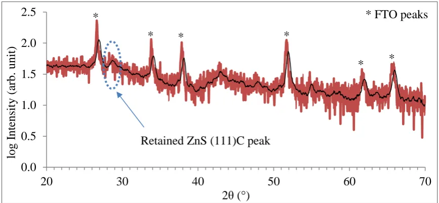
8 was observed. For the ZnS layers grown at 1430 mV, a retention of ZnS(111)C peak was obserced at 2θ=~29.0˚ with reduced of the peak intensity (see Figure 3 (b) and Figure 4).
Figure 4 shows the XRD spectra plotted in log-scale in order to identify all peaks. The slight shift towards lower 2θ angle of the ZnS (111)C after heat treatment indicates compressive stress formation in the deposited film and also possible change in chemical composition [26,27].
Figure 3: XRD patterns for ZnS layers grown between 1400 and 1460 mV cathodic voltages for (a) as-deposited and (b) heat treated at 300˚C for 10 minutes.
0 500 1000 1500 2000 2500 3000 3500 4000
20 30 40 50 60 70
XRD pe ak int ensit y (a rb. unit ) 2θ ˚ ZnS(111)C ZnS(101)H ZnS(002)H Zn(101)H ZnS(110)H ZnS(220)C FTO 1400 mV 1410 mV 1420 mV 1430 mV 1440 mV 1450 mV 1460 mV (a) As-deposited ZnO(101)H 0 500 1000 1500 2000 2500 3000 3500
20 30 40 50 60 70
XRD pe ak int ensit y (a rb. unit ) 2θ ˚ ZnS(111)C FTO 1400 mV 1410 mV 1420 mV 1430 mV 1440 mV 1450 mV 1460 mV (b) Heat treated
[image:9.595.87.521.134.504.2]9 The amorphisation of the crystalline ZnS grown at 1430 mV might be due to high defect concentration [13], elemental composition, oxidation, and the sublimation of the layer leading
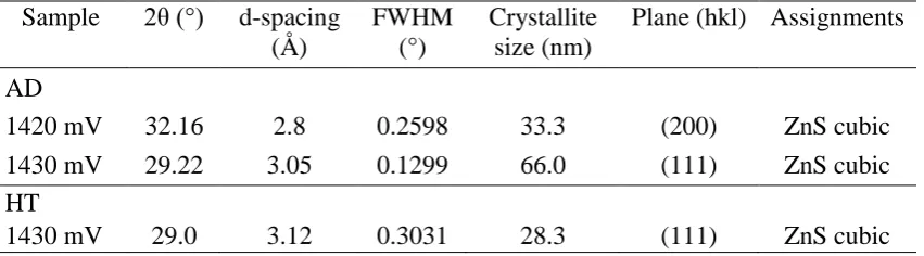
to the degradation of the ZnS layer. The crystallite size was calculated using the Scherrer's
formula (see equation (2)), where θ is the Bragg angle, β is the full-width-at-half-maximum
(FWHM) of the diffraction intensity in radians and λ is the wavelength of the X-rays used
(1.54 Å) and the XRD data is summarised in Table 1. The highest crystallite size of ~66 nm
was observed for the ZnS layers grown at 1430 mV. After heat treatment, a reduction in the crystallite size along the same plane was observed for the ZnS layers grown at 1430 mV due to deterioration of the ZnS layer [13]. This observation can be attributed to the re-crystallisation of ZnS resulting in the competing phases of hexagonal and cubic ZnS. Another possibility is the oxidation of ZnS surface to give ZnO with competing crystalline phases resulting to collapse of the ZnS crystallinity. The extracted XRD data from this ZnS material work matches the Joint Committee on Powder Diffraction Standards (JCPDS) reference file number 00-05-566, 00-05-492 and 00-36-1450 for ZnS, 00-036-1451 for ZnO and 00-004-0831 for Zn. The presence of the narrow crystalline range of electrodeposited ED-ZnS and the amorphisation of the ED-ZnS layers is very different to the ZnS layers electroplated from the bath incorporating complexing agents [9,11,12] with improvement in the ZnS layer crystallinity with the increasing complexing agent concentration [24].
cos 94 . 0
D (2)
0.0 0.5 1.0 1.5 2.0 2.5
20 30 40 50 60 70
log
I
ntensit
y
(a
rb.
unit
)
2θ (°) Retained ZnS (111)C peak
* * *
* *
*
[image:10.595.84.518.80.281.2]* FTO peaks
10 Figure 5 (a) and Figure 5 (b) show the Raman spectra of ~600 nm thick ZnS layers grown on glass/FTO substrates at 1420 mV, 1430 mV and 1440 mV cathodic voltages under as-deposited and heat treated conditions respectively. Raman peaks associated with ZnS were
observed at 147 cm-1 and 217 cm-1 which are identified as 2TA and 2LA optical mode
phonons. With respect to the as-deposited ZnS layers (Figure 5 (a)), sharp Raman peaks were
observed at 147 cm-1 and 217 cm-1 for the layers grown at 1420 mV and 1430 mV while
broad peaks were observed for the ZnS layers grown at 1440 mV. It should be noted that the ZnS layers grown at 1440 mV is similar to all the other explored ZnS layers (1400 to 1460) mV with the exception of 1420 mV and 1430 mV grown layers. As documented in the literature, the broadness of the observed peaks under as-deposited condition suggests the amorphous nature of the most of the ZnS layers which are in accord with the submissions made in the XRD section (see Section 3.2a) for ZnS [28,29]. While the observed broadening
of the peaks at 147 cm-1 and 217 cm-1 of the ZnS layers grown at 1420 mV and 1430 mV
[image:11.595.74.500.138.256.2]after heat treatment shows the amorphisation of the layers due to the randomisation of the crystal structure [30,31]. In addition, possible oxidation of the ZnS surface resulting into competing crystalline phases of ZnS and ZnO may occur and result to collapse of the crystalline structure.
Table 1: The XRD analysis of ZnS layers grown at cathodic voltages of 1420 mV and 1430 mV under both as-deposited and the heat treated conditions.
Sample 2θ (°) d-spacing
(Å)
FWHM (°)
Crystallite size (nm)
Plane (hkl) Assignments
AD
1420 mV 32.16 2.8 0.2598 33.3 (200) ZnS cubic
1430 mV 29.22 3.05 0.1299 66.0 (111) ZnS cubic
HT
11
3.3 Optical Analysis
Figure 6 (a) shows the optical absorbance measurement of ~200 nm thick ZnS layers grown between the (1410 and 1440) mV cathodic voltage under the as-deposited condition and
Figure 6 (b) after heat treatment at 300°C for 10 minutes. The absorbance squared (A2) was
plotted against the energy of photons and the extrapolated straight-line section of the graph to
the energy of photons axis (at A2=0) gives an estimate of the bandgap energy. With respect to
the as-deposited ZnS layers grown between (1410 and 1440) mV (Figure 6 (a)), the observed bandgap ranges between (3.70 and 3.85) eV. After heat treatment, an increase in the observed bandgap ≥3.84 eV and a reduction in the bandgap range between (3.84 and 3.94) eV were
observed. The deviation of the observed bandgap energy from that of the bulk cubic-ZnS of ~3. 70 eV [6] might be due to the incorporation of hexagonal ZnS which is known to have a bandgap of ~3.90 eV [32–34] (see Section 3.2). The non-conformity of deposited ZnS with 3. 70 eV bandgap norm has also been observed for layer grown from other techniques such as chemical bath deposition (CBD) [35] and metal organic vapour phase epitaxy (MOVPE) [36] amongst others.
Figure 5: Raman spectra of (a) as-deposited and (b) heat treated ZnS thin-films grown between (1420 and 1440) mV.
0 5000 10000 15000 20000
100 200 300 400 500 600
Intensit
y
(a
rb.
unit
)
Raman shift (cm-1)
0 5000 10000 15000 20000
100 200 300 400 500 600
Intensit
y
(a
rb.
unit
)
Raman shift (cm-1)
147 217
(a) As-deposited
(b) Heat treated
1430 mV
1420 mV
1440 mV
1430 mV
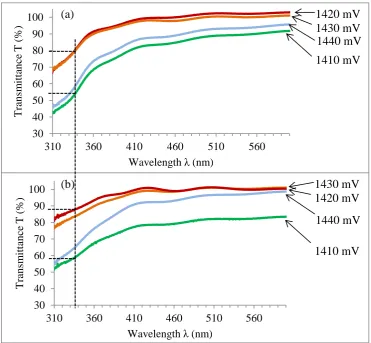
[image:12.595.116.487.76.359.2]12 Figure 7 (a) shows the transmittance of 150 nm thick ZnS layers grown between (1410 and 1440) mV under as-deposited and Figure 7 (b) after heat treatment at 300°C for 10 minutes. Comparatively, a slight increase in transmittance was observed for all the explored ZnS layers after heat treatment. It is noteworthy that all the samples show transmittance above 50% for wavelengths larger than 335 nm with the highest transmittance of ~80% observed for the layers grown at 1420 mV and 1430 mV. The ZnS layers grown at 1420 mV and 1430 mV shows high optical property suitable for a buffer layer in a photovoltaic device configuration with the negligible parasitic absorbance of incident photon to the cell.
0 5
2 2.5 3 3.5 4 4.5
A
2 (a
rb. un
it
)
Photon energy (hv) (a) As-deposited
1430 mV 1410 mV
1440 mV 1420 mV
0 5
2 2.5 3 3.5 4 4.5
A
2(a
rb. un
it
)
Photon energy (hv) (b) Heat treated
1410 mV 1430 mV
1440 mV 1420 mV
[image:13.595.114.485.74.419.2]13
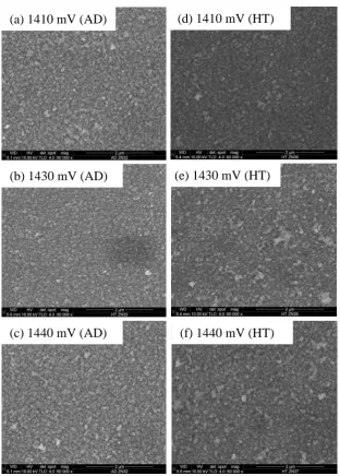
3.4 Morphological and Compositional Analysis
Figure 8 (a), Figure 8 (b) and Figure 8 (c) show the SEM micrographs of as-deposited ZnS layers grown at 1410 mV, 1430 mV and 1440 mV respectively, while Figure 8 (d), Figure 8 (e) and Figure 8 (f) show their respective heat treated micrographs. For this set of experiments, the ZnS layers utilised were ~200 nm thick grown on glass/FTO. For the explored cathodic voltages range between (1410 to 1440) mV under both the as-deposited and heat treated conditions, full coverage of the underlying glass/FTO substrate was observed. A slight increase in the grain sizes of the as-deposited ZnS layers ranging from ~(100 to 380) nm to ~(120 to 400) nm after heat treatment was observable. Further to this, it appears that grains of the ZnS layers grown at 1430 mV and 1440 mV coalesce after heat treatment. 30 40 50 60 70 80 90 100
310 360 410 460 510 560
T rans m it tanc e T ( % )
Wavelength λ (nm)
(a) 1420 mV
1430 mV 1440 mV 1410 mV 30 40 50 60 70 80 90 100
310 360 410 460 510 560
T rans m it tanc e T ( % )
Wavelength λ (nm)
(b) 1430 mV
1420 mV 1440 mV
1410 mV
[image:14.595.101.473.70.413.2]14
3.5 Electrical Property Analyses
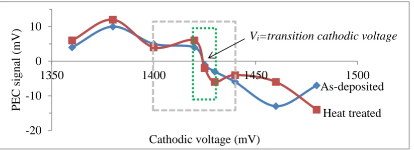
The plot of the PEC signals against the cathodic voltage range of (1360 to 1480) mV from which the ZnS layers were grown is shown in Figure 9. It should be noted that prior to PEC measurement, a semiconductor with a known conduction type was measured to calibrate the PEC cell measurement system. From observation, both the as-deposited and the annealed ZnS
layers show a similar trend with a transition from p-ZnS to n-ZnS between (1420 and 1430)
mV. As documented in the literature, the richness of sulphur in ZnS results in the p-type
conductivity of ZnS, while the n-type conduction of ZnS is associated with zinc-richness
[15]. It should be taken into consideration that the transition cathodic voltage from p- to
n-type conduction n-type is the voltage from which stoichiometric ZnS is obtainable with 1:1 Figure 8: SEM micrographs of as-deposited (AD) and heat treated ZnS layers
grown between (1420 and 1440) mV. (a) 1410 mV (AD)
(e) 1430 mV (HT) (b) 1430 mV (AD)
(d) 1410 mV (HT)
[image:15.595.124.437.73.510.2]15 atomic ratio of Zn to S in the layer. Based on the observations made on the PEC result, it can be inferred that the crystallinity ZnS layers can be grown close to the transition cathodic voltage as discussed in Section 3.2.
Consequently, there is a possible few millivolts (mV) shift in either direction from time to
time due to bath replenishment with either Zn2+ or S2- ions. It is however important that the
transition (intrinsic) cathodic voltage (Vi) is known as it serves as a point of reference.
Furthermore, the observed PEC signal magnitude is comparatively low as compared to the other electrodeposited semiconductors materials [37,38]. This observation could be attributed to the wide bandgap nature of ZnS resulting in the transmission of most of the visible light [15,39] with low absorption.
Prior to DC conductivity measurement, Ohmic contacts were formed on both the p-ZnS and n-ZnS layers by respectively depositing 100 nm gold (Au) or indium (In) on the ZnS layers to
form glass/FTO/p-ZnS/Au or glass/FTO/n-ZnS/In. The ZnS layers utilised for the DC conductivity measured were ~1 μm thick each. The resistivity ρ was estimated using equation
(3) where R is the resistance, A is the contact area, L is the film thickness and σ is the
electrical conductivity. The electrical resistance (R) of the structure was calculated from the Ohmic I-V data obtained under dark condition.
1
L RA
(3)
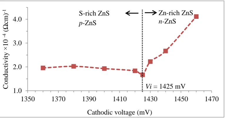
Figure 10 shows the graphical plot of conductivity against the growth voltage of ZnS layers after heat treatment. The large bandgap of ~(3.70-3.90) eV is an indication of the electrical property of ZnS tending towards insulation. A noticeable trend showing a gradual reduction Figure 9: PEC signals for ZnS layers grown between 1360 mV and 1480 mV cathodic voltages under both as-deposited and heat treated conditions.
-20 -10 0 10
1350 1400 1450 1500
P
EC
sig
na
l
(mV
)
Cathodic voltage (mV)
As-deposited
[image:16.595.95.507.148.298.2]16 in electrical conductivity value from the ZnS layers grown at 1360 mV towards the ZnS layer grown at 1425 mV was observed in Figure 10. Conversely, a gradual increase in the electrical conductivity was observed with increasing cathodic voltage at which the ZnS layers were grown.
In relation to the cathodic voltage-dependent deposition sequence as discussed in Section 3.1, the observed trend in Figure 10 can be attributed to the deposition of S-rich ZnS layers at cathodic voltages lower than ~1425 mV and the increasing Zn-richness of the ZnS layers grown above 1425 mV. It is clear that the ZnS layers grown close to 1425 mV show relatively lowest conductivity due to the stoichiometric and the intrinsic nature of the ZnS layers grown since practically all valence electrons are engaged in bonding.
3.6 Solar cell device characterisation
The I-V measurements for the glass/FTO/n-ZnS/n-CdS/n-CdTe/Au devices incorporating both c-ZnS and a-ZnS buffer layers were performed under both dark and AM1.5 illuminated
condition. Under dark condition, parameters derived include shunt resistance (Rsh), series
resistance Rs, rectification factor RF, reverse saturation current Io, ideality factor n, and the
potential barrier height ɸb. The effective Richardson constant (A*) for CdTe was calculated to
be 12 Acm-2K-2 using equation (4), where m* is the effective electron mass and h is the
Planck’s constant (6.626×10⁻³⁰ cm2kgs-1). Depending on the conductivity type of the
semiconductor, the effective electron mass can be denoted as me*or mp* for n-type and p-type
[image:17.595.111.494.170.372.2]semiconductor materials respectively.
Figure 10: A typical graph of electrical conductivity against growth voltage of heat treated ZnS layers.
1.0 2.0 3.0 4.0
1350 1370 1390 1410 1430 1450 1470
Conduc
tivi
ty
×
10
-4
(Ω
cm)
-1
Cathodic voltage (mV)
Vi = 1425 mV S-rich ZnS
p-ZnS
17 3 2 * * 4 h q k m
A (4)
From the I-V measurement under the illuminated AM1.5 condition for the
glass/FTO/n-ZnS/n-CdS/n-CdTe/Au devices, parameters such as short-circuit current density Jsc,
open-circuit voltage Voc, fill-factor FF and efficiency η were derived.
Figure 11 (a-b) show the I-V curves of glass/FTO/n-ZnS/n-CdS/n-CdTe/Au device incorporating c-ZnS [18] or a-ZnS buffer layers under dark condition plotted in linear-linear and log-linear scales, while Figure 11 (c) shows the I-V curves plotted under illuminated AM1.5 condition. The obtained electronic parametric quantities of the glass/FTO/n-ZnS/n-CdS/n-CdTe/Au photovoltaic cells are summarised in Table 2.
With respect to the observation in Figure 11 (a-b) and the dark I-V section in Table 2, the
[image:18.595.88.495.294.707.2]significantly high Rsh values recorded for the glass/FTO/n-ZnS/n-CdS/n-CdTe/Au devices
Figure 11: I–V characteristics of glass/FTO/n-ZnS/n-CdS/n-CdTe/Au devices
incorporating c-ZnS or a-ZnS buffer layers plotted under dark condition plotted in (a) Linear-linear scale (b) Log-linear scale and (c) I-V plotted under illuminated AM1.5
0 1 2 3 4 5 6
-1 -0.5 0 0.5 1
C urr ent × 10 -4 (A ) Bias (V) c-ZnS a-ZnS (a) -10 -8 -6 -4
-2 0 0.5 1
log
I
Bias voltage (V) c-ZnS a-ZnS (b) -35 -25 -15 -5 5
-0.2 0 0.2 0.4 0.6 0.8
18 indicate the absence of shunt paths which might be as a result of the ZnS buffer layer integrated into the device even with the thinning down of the CdS layer to 65 nm [8]. This indicates the provision of a good substrate for CdS and CdTe layers to grow with improved
material qualities. High Rsh values in photovoltaic devices have also been associated with the
quality of the deposited semiconductor layer with regards to the absence of gaps, voids and
high dislocation density in the electroplated semiconductor material [40]. Both the Rsh values
of the glass/FTO/n-ZnS/n-CdS/n-CdTe/Au incorporating both c-ZnS and a-ZnS buffer layers are comparable. This indicates the provision of a good substrate for CdS and CdTe to grow with improved material qualities.
Considerably high Rs values of 470 Ω and 637 Ω for both devices respectively incorporating
c-ZnS and a-ZnS buffer layers were observed which do have an adverse effect on all solar
cell parameters. For both of the devices under consideration incorporating c-ZnS and a-ZnS
buffer layers, outstanding Rectification Factor RF with values exceeding 104 was observed.
As documented in the literature, RF values exceeding 103 is considered as one of the
characteristic property of high-efficiency photovoltaic cell [10]. Additionally, the observed
ideality factor n within the 1.00 and 2.00 range, signifies that both thermionic emission and
recombination & generation (R&G) processes taking place in parallel are the dominating
current transport mechanism of the devices [2,41,42]. For devices with n>2.00, the current
transport mechanisms are associated with thermionic emission, R&G and tunnelling of
electrons with high energy through the barrier height [43] resulting in the under estimation of
the barrier height ɸb. High n>2.00 may also be dependent on the doping levels on both sides
of the junction and on the interface charges of an hetero-junction device structure [44]. It
should be taken into consideration that the estimated potential barrier heightɸb of >0.82 eV
and >0.79 eV for respective devices incorporating c-ZnS and a-ZnS buffer layers may be
19 With respect to Figure 11 (c) and the AM1.5 illuminated condition section of Table 2,
parameters derived include the short-circuit current density Jsc, open-circuit voltage Voc, fill
factor FF, and the conversion efficiency η. For the glass/FTO/n-ZnS/n-CdS/n-CdTe/Au
devices incorporating c-ZnS buffer layers, the derived parameters include the Jsc=34.08
mAcm-2, Voc=730 mV, FF=0.57 and the η=14.18%. While the derived parameters for the
devices incorporating a-ZnS include Jsc=29.94 mAcm-2, Voc=720 mV, FF=0.52 and the
η=11.21%. All four parameters have improved when c-ZnS buffer layer is used. For both
devices, the observed Jsc values are higher than the Shockley–Queisser limit for single p-n
junction [45]. The high Jsc observation is attributable to the multilayer graded bandgap
[image:20.595.125.471.151.507.2]configuration [46] utilised in this work. This observation have also been documented and backed by the literatures for inorganic [47,48] and hybrid [49] solar cell technologies. Theoretically, it has been proved that graded bandgap solar cell configurations are capable of Table 2: Summary of device parameters obtained from I-V (both under illuminated and dark conditions) and C-V (dark condition) for crystalline ZnS (c-ZnS) and amorphous ZnS (a-ZnS) incorporated in glass/FTO/n-ZnS/n-CdS/n-CdTe/Au solar cell.
ZnS structure
Parameters c-Zns a-ZnS
I-V measurement under dark condition
Rsh (Ω) >106 >106
Rs (Ω) 470 637
log (R.F.) 4.8 4.2
Io (A) 1.0×10⁻⁹ 1.2×10⁻⁹
n 1.60 1.85
Φb (eV) >0.82 >0.79
I-V measurement under AM1.5 illuminated condition
Isc (mA) 1.07 0.94
Jsc (mAcm-2) 34.08 29.94
Voc (mV) 730 720
Fill-factor 0.57 0.52
Efficiency (%) 14.18 11.21
DC and C-V measurements under dark condition
ρ×103 (Ω.cm) 1.13 1.13
Co (pF) 280 340
Vbi (eV) 1.10 1.07
(ND-NA) (cm-3) 7.79×10¹⁴ 9.52×10¹⁴
(EC-EF) eV ~0.17 ~0.21
W (nm) 1092.2 899.5
20 attaining a conversion efficiency of ~38% under AM1.5 [50,51] as compared to the 23% of
single p-n junction solar cells [45]. Harvesting more photons, the contribution of “impurity
PV effect” and “impact ionisation” observed in the graded bandgap devices as described in
[image:21.595.170.454.404.593.2]Ref [47,48] can be the explanation for this increase in Jsc values.
Figure 12 shows the Mott-Schottky plots of C-2 against V for the
glass/FTO/n-ZnS/n-CdS/n-CdTe/Au devices incorporating c-ZnS or a-ZnS layers measured under dark condition. The
derived parameters from the C-V and C-2-V plots include capacitance at zero bias C
o, Fermi
level position (EC-EF), built-in potential Vbi, doping concentration of the material ND-NA,
barrier height Φb, depletion layer width at zero bias W and charge carrier mobility µ﬩.
Pertaining to Figure 12, a slightly stable and similar capacitance of ~280 pF and 340 pF for devices incorporating c-ZnS or a-ZnS layers were observed from the reverse bias region of -1
V, through the Co up to ~0.5 V in the forward bias region. The constant capacitance signifies
that the glass/FTO/n-ZnS/n-CdS/n-CdTe/Au devices are fully depleted in which the depletion width W is larger or comparable to the device thickness of ~1.0 µm at reverse bias region up to ~0.5 V in the forward bias region.
With increasing forward bias voltage above 0.5 V, increase in the measured capacitance resulting in a gradual reduction of the depletion width was observed for both of the devices under consideration. The varying capacitance in the forward bias region was used to plot the Mott-Schottky graph and approximate values of the parameters for the material and the
0.0 0.2 0.4 0.6 0.8 1.0 1.2 1.4
-1 -0.5 0 0.5 1
C
-2
×
10
19
(F
-2)
Bias voltage (V)
a-ZnS c-ZnS
21 device. Since the capacitance values depend on defects in the structure, the parameters obtained are not very accurate, but helpful in understanding the devices.
The depletion width of 1092 nm and 899.5 nm for the respective devices incorporating c-ZnS and a-ZnS at zero bias was calculated using equation (5). From observation, the calculated W
for the two devices incorporating c-ZnS and a-ZnS shows a more similar width to the
thickness of the device (~1150 nm). From the Mott-Schottky plot (see Figure 12) and
equations (5)-(8), both the Vbi and (ND-NA) can be determined. In these equations, the
capacitance is C, built-in potential is Vbi, the reverse bias voltage is VR, the contact area is A,
the electronic charge is e, the permittivity of free space is εo, semiconductor permittivity is εs
and dielectric constant (or relative permittivity) is εr. based on the literature, εr is ~11 [52].
The gradient acquired from the intercept of the Mott-Schottky plot with the bias-axis (see Figure 12) was incorporated into equation (7).
The noticeable constant C-2 capacitance in the Mott-Schottky plot of both the devices
indicates that both devices are fully depleted. Therefore, the doping concentration (ND-NA)
can only be evaluated from the data in the forward bias voltage of ~0.5 V and beyond. The
calculated doping densities of 7.79×1014 cm-3 and 9.52×1014 cm-3 for the devices respectively
incorporating c-ZnS and a-ZnS buffer layers are primarily within the n-CdTe layers, which is
the bulk of the device. The slight difference in the (ND-NA) associated with n-CdTe can be
due to the substrate quality provided by the initial ZnS layers for the CdS and CdTe layers to grow with less defect. For both of the devices, the calculated values of the doping concentrations and the built-in potential are in line with the values of high-efficiency
CdTe-based devices (~1.0 × 10¹⁴ to 5 × 10¹⁵) cm-3 in the literature [3,53,54]. The effective density
of states in the conduction band (Nc) was calculated to be ~7.92×1017 cm-3 using equation (9)
where h is the Plank's constant, T is the temperature, k is the Boltzmann’s constant and me* is
the effective electron mass. With the assumption that all donor atoms (ND) are ionised (n≈ND)
W
C r 0
0 (5) ) ( 2 2 2 bi R D s V V N eA
C
(6) 2 2 A eN slope D s (7) slope eA N o r D
22
[image:22.595.234.498.329.491.2]22
at room temperature, the charge carrier mobilities µ﬩ were estimated using equation (10) to
give (7.07 and 5.78) cm2V-1s-1 for devices incorporating c-ZnS or a-ZnS layers respectively.
It should be noted that the same electrical conductivity of 8.82×10⁻⁴ (Ωcm)-1 utilised was
estimated from the dark I-V curves of glass/FTO/n-CdTe with Ohmic indium contacts.
4 Conclusion
This work demonstrates the successful deposition of both p- and n-type ZnS thin-films from
an aqueous solution containing 0.2 M ZnSO4·H2O and 0.2 M (NH4)2S2O3 using two-electrode
electroplating configuration. Based on the selected material characterisation techniques explored, a narrow range of 1420 mV to 1430 mV was identified as the cathodic potential in which crystalline ED-ZnS is achievable. The XRD results show the amorphisation of the as-deposited crystalline ED-ZnS layer after 300°C heat treatment and the retention of crystallinity of the ED-ZnS layers grown at (~1425 to ~1430) mV. The SEM micrographs show small grain attesting to the wetting property of ZnS. The optical bandgap of the ED-ZnS layers is within the reported values for hexagonal ED-ZnS layers (~3.90 eV). The fabricated devices using ZnS as the buffer layer in the glass/FTO/n-ZnS/n-CdS/n-CdTe/Au graded bandgap configuration show prospect of achieving even higher photovoltaic efficiency. The graded bandgap increases the possibility of harnessing more photons both from the blue-end
and the red-end of the solar spectrum. The device parameters observed incorporating c-ZnS
are much better (η=14.2%) than those devices fabricated with a-ZnS (11.2%). Work is
on-going on the optimisation of other processing and device fabrication steps towards achieving higher efficiency.
Acknowledgement
The authors would like to acknowledge Ashfaq and other members of SHU Solar Energy Group for their contributions. The principal author wishes to appreciate SHU, EKSU and TETFUND for their backing in undertaking this research.
2 3
2 2 2
h kT m
Nc e (9)
e ND
23
References
1. T. N. and M. Mizutani, Jpn. J. Appl. Phys. 41, L165 (2002).
2. S. M. Sze and K. K. Ng, Physics of Semiconductor Devices (John Wiley & Sons, Inc., Hoboken, NJ, USA, 2006).
3. J. Britt and C. Ferekides, Appl. Phys. Lett. 62, 2851 (1993).
4. T. L. Chu, S. S. Chu, C. Ferekides, C. Q. Wu, J. Britt, and C. Wang, J. Appl. Phys. 70,
7608 (1991).
5. J. E. Granata and J. R. Sites, Conf. Rec. Twenty Fifth IEEE Photovolt. Spec. Conf. 1996 853 (2000).
6. T. Yasuda, K. Hara, and H. Kukimoto, J. Cryst. Growth 77, 485 (1986).
7. A. Ennaoui, W. Eisele, M. Lux-Steiner, T. P. Niesen, and F. Karg, Thin Solid Films 431–
432, 335 (2003).
8. A. A. Ojo, H. I. Salim, O. I. Olusola, M. L. Madugu, and I. M. Dharmadasa, J. Mater. Sci.
Mater. Electron. 28, 3254 (2017).
9. E. M. Mkawi, K. Ibrahim, M. K. M. Ali, M. A. Farrukh, and A. S. Mohamed, J. Electron.
Mater. 44, 3380 (2015).
10. I. M. Dharmadasa, Advances in Thin-Film Solar Cells (Pan Stanford, Singapore, 2013).
11. S. Tec-Yam, J. Rojas, V. Rejón, and a. I. Oliva, Mater. Chem. Phys. 136, 386 (2012).
12. G. L. Agawane, S. W. Shin, A. V. Moholkar, K. V. Gurav, J. H. Yun, J. Y. Lee, and J. H.
Kim, J. Alloys Compd. 535, 53 (2012).
13. B. W. Sanders and A. H. Kitai, J. Cryst. Growth 100, 405 (1990).
14. O. K. Echendu and I. M. Dharmadasa, J. Electron. Mater. 43, 791 (2013).
15. M. L. Madugu, O. I.-O. Olusola, O. K. Echendu, B. Kadem, and I. M. Dharmadasa, J.
Electron. Mater. 45, 2710 (2016).
16. N. B. Chaure, A. P. Samantilleke, R. P. Burton, J. Young, and I. M. Dharmadasa, Thin
24
17. A. A. Ojo, I. O. Olusola, and I. M. Dharmadasa, Mater. Chem. Phys. 196, 229 (2017).
18. A. A. Ojo and I. M. Dharmadasa, Sol. Energy 158, 721 (2017).
19. N. A. Abdul-Manaf, A. R. Weerasinghe, O. K. Echendu, and I. M. Dharmadasa, J. Mater.
Sci. Mater. Electron. 26, 2418 (2015).
20. H. I. Salim, V. Patel, a. Abbas, J. M. Walls, and I. M. Dharmadasa, J. Mater. Sci. Mater.
Electron. 26, 3119 (2015).
21. I. M. Dharmadasa, a B. McLean, M. H. Patterson, and R. H. Williams, Semicond. Sci.
Technol. 2, 404 (1987).
22. Y. GUO and X. DENG, Sol. Energy Mater. Sol. Cells 29, 115 (1993).
23. M. P. R. Panicker, J. Electrochem. Soc. 125, 566 (1978).
24. P. U. Londhe, A. B. Rohom, G. R. Bhand, S. Jadhav, M. G. Lakhe, and N. B. Chaure, J.
Mater. Sci. Mater. Electron. 28, 5207 (2017).
25. A. Goudarzi, A. D. Namghi, and C.-S. Ha, RSC Adv. 4, 59764 (2014).
26. J. Fang, P. H. Holloway, J. E. Yu, K. S. Jones, B. Pathangey, E. Brettschneider, and T. J.
Anderson, Appl. Surf. Sci. 70–71, 701 (1993).
27. F. Bittau, A. Abbas, K. L. Barth, J. W. Bowers, and J. M. Walls, Thin Solid Films 633, 92
(2017).
28. A. Fairbrother, V. Izquierdo-Roca, X. Fontané, M. Ibáñez, A. Cabot, E. Saucedo, and A.
Pérez-Rodríguez, CrystEngComm 16, 4120 (2014).
29. Y. Ebisuzaki and M. Nicol, J. Phys. Chem. Solids 33, 763 (1972).
30. H. Richter, Z. P. Wang, and L. Ley, Solid State Commun. 39, 625 (1981).
31. I. H. Campbell and P. M. Fauchet, Solid State Commun. 58, 739 (1986).
32. T. Ben Nasr, N. Kamoun, M. Kanzari, and R. Bennaceur, Thin Solid Films 500, 4 (2006).
33. A. Torabi and V. N. Staroverov, J. Phys. Chem. Lett. 6, 2075 (2015).
25 Boston, MA, 2006), pp. 325–342.
35. T. Nakada, M. Mizutani, Y. Hagiwara, and A. Kunioka, Sol. Energy Mater. Sol. Cells 67,
255 (2001).
36. R. Nomura, T. Murai, T. Toyosaki, and H. Matsuda, Thin Solid Films 271, 4 (1995).
37. A. A. Ojo and I. M. Dharmadasa, J. Mater. Sci. Mater. Electron. 28, 14110 (2017).
38. O. K. Echendu, K. B. Okeoma, C. I. Oriaku, and I. M. Dharmadasa, Adv. Mater. Sci.
Eng. 2016, 1 (2016).
39. A. B. Bhalerao, C. D. Lokhande, and B. G. Wagh, IEEE Trans. Nanotechnol. 12, 996
(2013).
40. T. Soga, Elsvier Sci. 614 (2006).
41. A. Neugroschel, F. A. Lindholm, and Chih-Tang Sah, IEEE Trans. Electron Devices 24,
662 (1977).
42. M. A. Wolf and M. Wolf, IEEE Trans. Electron Devices 32, 800 (1985).
43. J. Verschraegen, M. Burgelman, and J. Penndorf, Thin Solid Films 480–481, 307 (2005).
44. M. Abdel Naby, A. Zekry, F. El Akkad, and H. F. Ragaie, Sol. Energy Mater. Sol. Cells
29, 97 (1993).
45. W. Shockley and H. J. Queisser, J. Appl. Phys. 32, 510 (1961).
46. A. De Vos, J. Phys. D. Appl. Phys. 13, 839 (2000).
47. I. M. Dharmadasa, O. Elsherif, and G. J. Tolan, J. Phys. Conf. Ser. 286, 012041 (2011).
48. I. M. Dharmadasa, A. A. Ojo, H. I. Salim, and R. Dharmadasa, Energies 8, 5440 (2015).
49. I. M. Dharmadasa, Sol. Energy Mater. Sol. Cells 85, 293 (2005).
50. M. Wolf, Proc. IRE 48, 1246 (1960).
51. P. R. Emtage, J. Appl. Phys. 33, 1950 (1962).
26 53. T. Potlog, L. Ghimpu, P. Gashin, a. Pudov, T. Nagle, and J. Sites, Sol. Energy Mater.
Sol. Cells 80, 327 (2003).