Development of nanostructured PVD coatings for total
knee replacement joints using HIPIMS.
SUGUMARAN, Arunprabhu A.
Available from Sheffield Hallam University Research Archive (SHURA) at:
http://shura.shu.ac.uk/19288/
This document is the author deposited version. You are advised to consult the
publisher's version if you wish to cite from it.
Published version
SUGUMARAN, Arunprabhu A. (2014). Development of nanostructured PVD coatings
for total knee replacement joints using HIPIMS. Doctoral, Sheffield Hallam University
(United Kingdom)..
Copyright and re-use policy
Sheffield Haliarn university Learning and Inform' n Services
A dsetts C entre, City C am pus Sheffield S1 1WD
ProQuest Number: 10694168
All rights reserved
INFORMATION TO ALL USERS
The quality of this reproduction is dependent upon the quality of the copy submitted.
In the unlikely event that the author did not send a com plete manuscript and there are missing pages, these will be noted. Also, if material had to be removed,
a note will indicate the deletion.
uest
ProQuest 10694168
Published by ProQuest LLC(2017). Copyright of the Dissertation is held by the Author.
All rights reserved.
This work is protected against unauthorized copying under Title 17, United States C ode Microform Edition © ProQuest LLC.
ProQuest LLC.
789 East Eisenhower Parkway P.O. Box 1346
Development of Nanostructured PVD Coatings
for Total Knee Replacement Joints using
HIPIMS
Arunprabhu Arunachalam Sugumaran
A thesis submitted in partial fulfilment of the requirements of
Sheffield Hallam University for the degree of
Doctor of Philosophy
ACKNOWLEDGEMENTS
Acknowledgements
At first, I would like to thank my Director of Studies Prof. Papken Hovsepian
for his invaluable guidance and encouragement throughout the course of my studies
without which, I would have not been able to produce this piece of work. I would also
like to thank Prof. Arutiun Ehiasarian (Supervisor II) for his help in plasma analysis
and writing research articles. I am grateful to Dr. Imran Khan (Supervisor II), Director
of Research, Biomet, UK for providing me with the test components.
Special thanks to Dr. Yashodhan Purandare for his assistance in handling the
PVD system and other analytical instruments. I greatly appreciate Mr. Gary Robinson
for his technical support in preparing the test samples. Special thanks to Mr. Daniel
Loch also for his help in plasma diagnostics and other useful suggestions.
I acknowledge the MERI for providing me with the lab facilities and financial
support to carry out this research work. I thank Mr. Stuart Creasy and Mr. Vinay Patel
for their support in handling the electron microscope. I am grateful to all my teachers
and professors who helped me to grow up to this stage.
Thanks to fellow MERI members Dr. Vikas Kumar, Ms. Anna Oniszczuk,
Dr. Chinh Nguyen, Mr. Sampan Seth, Ms. Paranjayee Mandal, Mr. Thomas Morton,
Mr. Stephen Dodds, Mr. Itai Vutabwarova, Mrs. Trinh Pham and Dr. Ganesh Kamath
for their support.
It's a pleasure to thank my beloved grandparents for their everlasting love and
support. Special thanks to my uncles, Mr. S. Ramachandran, Mr. M. Thangarajan who
have been very helpful and supportive throughout my career. I would like to thank my
friends Dr. K. Sasipriya and Ms. P. Kiruthika Devi for their moral support. Finally, I
Abstract
TABLE OF CONTENTS
Contents
Acknowledgements...I Abstract... II Contents...Ill List of Acronyms...VII
Chapter 1 ...1
1 Introduction... 1
1.1 Motivation... 1
1.1.1 Human knee joint...1
1.1.2 Knee replacement joints... 2
1.1.3 Limitations of existing metallic biomedical materials...3
1.2 Surface engineering of implants...4
1.2.1 High Power Impulse Magnetron Sputtering...5
1.3 Present research work... 6
1.3.1 Aims & Objectives...6
References... 8
Chapter 2 ... 11
2 Literature Review...11
2.1 Plasma & Glow discharge... 11
2.1.1 Ionisation... 12
2.1.2 Excitation... 13
2.1.3 Relaxation... 13
2.1.4 Recombination... 14
2.1.5 Classical DC glow discharge...14
2.2 Thin film deposition techniques...15
2.2.1 Physical Vapour Deposition...15
2.3 Cathodic arc deposition... 29
2.4 Microstructure evolution during coating growth... 31
2.4.1 Effect of sputtering parameters on microstructure evolution...33
2.5 Nano structured coatings for implants...38
TABLE OF CONTENTS
Chapter 3 ... 53
3 Materials and Methods... 53
3.1 Materials, Substrate preparation and deposition of various coatings... 53
3.1.1 Substrate materials...53
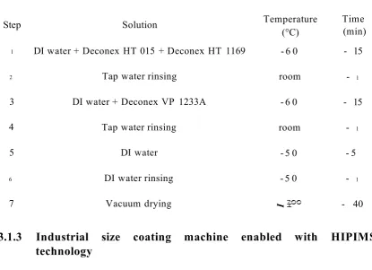
3.1.2 Substrate preparation prior to coating deposition...54
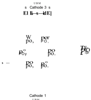
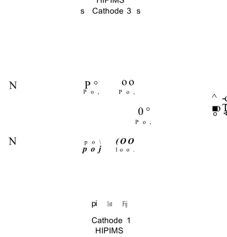
3.1.3 Industrial size coating machine enabled with HIPIMS technology...54
3.1.4 Protocol followed for the experiments...56
3.1.5 Deposition of TiN coatings... 57
3.1.6 Deposition of TiN/NbN multilayer coatings... 60
3.1.7 Deposition of TiCN/NbCN multilayer coating...61
3.1.8 Deposition of CrN/NbN multilayer coating... 62
3.2 Plasma diagnostics...63
3.3 Thin film characterisation techniques... 66
3.3.1 X-ray Diffraction analysis... 66
3.3.2 Determination of adhesion strength of thin film s... 69
3.3.3 Nanohardness measurement...71
3.3.4 Tribological characterisation...73
3.3.5 Determination of surface roughness...75
3.3.6 Energy Dispersive X- ray spectroscopy... 76
3.3.7 Microstructural analysis... 77
3.3.8 Electrochemical corrosion testing... 80
3.3.9 Raman spectroscopy...82
References... 85
Chapter 4 ... 88
4 Results and Discussion...88
4.1 Plasma analysis using Optical emission spectroscopy...88
4.1.1 Effect of different HIPIMS/UBM source combinations on {Ti1+} and {Ti0}...89
4.1.2 Effect of coil current on the degree of metal flux in the plasma generated by utilising different source combinations... 90
4.1.3 Effect of N2 flow on the degree of metal flux and N2 0 in the plasma generated by utilising different source combinations... 92
TABLE OF CONTENTS
4.5 Mechanical and tribological properties of TiN coatings...101
4.5.1 Nano-hardness test... 101
4.5.2 Coefficient of friction and wear coefficient... 102
4.6 Microstructure evolution...106
4.6.1 Effect of the degree of HIPIMS utilisation on the microstructure of TiN coatings... 106
4.6.2 Effect of bias voltage on the micro structure of TiN coatings...107
4.6.3 Effect of coil current on the microstructure of TiN coatings...108
4.7 Determination of residual stress in TiN coatings...110
4.7.1 Effect of the degree of HIPIMS utilisation on residual stress in TiN coatings ...110
4.7.2 Effect of coil current on residual stress in TiN coatings... 112
4.7.3 Effect of bias voltage on residual stress in TiN coatings... 114
4.8 Effect of bias voltage on the texture evolution of TiN coatings...118
4.9 Effect of degree of HIPIMS utilisation on the surface roughness of TiN coatings... 122
4.10 Effect of the degree of HIPIMS utilisation on corrosion resistance of TiN coatings... 124
4.10.1 Potentiodynamic polarisation measurements...124
4.10.2 SEM investigation of corroded sam ples...125
4.10.3 Raman spectroscopy... 126
4.10.4 Transmission electron microscopy... 130
4.11 Investigation of corrosion performance of TiN coatings deposited by arc evaporation and HIPIMS techniques...131
4.11.1 Potentiodynamic polarisation measurements of TiN coatings deposited using cathodic arc evaporation and 2HIPIMS + 2UBM source combination... 132
4.11.2 SEM analysis of TiN coatings deposited by arc evaporation method .... 134
4.11.3 Raman analysis of TiN coatings deposited by arc evaporation method and combined HIPIMS/UBM coating...137
4.12 Summary of TiN coatings... 139
4.13 Characterisation of TiN/NbN multilayer coatings... 141
4.13.1 Adhesion strength...141
4.13.2 X-ray diffraction analysis...142
4.13.3 Bilayer thickness...143
TABLE OF CONTENTS
4.13.5 Microstructure analysis...145
4.13.6 Mechanical and tribological properties...146
4.13.7 Corrosion properties... 147
4.14 Characterisation of TiCN/NbCN multilayer coatings...148
4.14.1 X-ray diffraction analysis... 148
4.14.2 Bilayer thickness... 149
4.14.3 Energy dispersive X-ray spectroscopy analysis... 149
4.14.4 Mechanical and tribological properties... 150
4.14.5 Corrosion properties...152
4.15 Characterisation of CrN/NbN multilayer coatings... 153
4.15.1 Adhesion strength...153
4.15.2 X-ray diffraction analysis...154
4.15.3 Energy dispersive X-ray spectroscopy analysis...155
4.15.4 Microstructure analysis... 156
4.15.5 Investigation of thickness distribution across the sample holder 156 4.15.6 Mechanical and tribological properties...158
4.15.7 Corrosion properties...160
4.16 Summary of multilayer coatings... 161
References... 162
Chapter 5 ... 166
5 Conclusions... 166
Future work...171
LIST OF ACRONYMS
List of Acronyms
PVD Physical Vapour Deposition
DCMS Direct Current Magnetron Sputtering
UBM Unbalanced Magnetron
HIPIMS High power impulse Magnetron sputtering
TKR Total Knee joint Replacement
UHMWPE Ultra-High Molecular Weight Polyethylene
CVD Chemical Vapour Deposition
E-beam Electron beam
AC Alternating Current
RF Radio Frequency
DLC Diamond Like Carbon
DI De-Ionized
HSS High Speed Steel
SS Stainless Steel
OES Optical Emission Spectroscopy
CCD Charge-Coupled Device
PMT Photo Multiplier Tube
EDS Energy Dispersive X-ray Spectroscopy
XRD X-Ray Diffraction
BB Bragg-Brentano
GA Glancing Angle
LA Low Angle
COF Coefficient of Friction
COW Coefficient of Wear
SEM Scanning Electron Microscope
CHAPTER 1 INTRODUCTION
Chapter 1
1 Introduction
1.1 Motivation
1.1.1 Human knee joint
Human knee joint is the largest hinge type and most complex synovial joint in
the body. It is formed by the tibia (shinbone), femur (thighbone) and patella (knee cap).
In addition, two fibrocartilaginous menisci improve congruency between the femur and
tibia during joint movements. The knee joint is reinforced by collateral ligaments and
two very strong cruciate ligaments that help provide smooth motion to the joint. A
salient feature of synovial joint is the existence of lubricating synovial fluid in the
synovial cavity around the articulating surfaces [1,2].
Intercondy'*
Patella
Surface for — articulation with patella
Posterior cruciate ligament
Flat surfaces for articulation with tibia in extension
Meniscus
Anterior cruciate ligament
-1—<r*— Round surfaces for
jjfy articulation with tibia in flexion
CHAPTER 1 INTRODUCTION
1.1.2 Knee replacement joints
A human knee joint affected by degenerative diseases such as osteoarthritis
(inflammation, pain and loss in function) loses its inherent mechanical properties due to
the excessive loading or lack of natural biological self-curing process. Moreover
diseases like osteoporosis (weakening of the bones) and trauma can also affect the
normal functioning of the knee [3]. These diseases may lead to knee arthroplasty which
is a surgical procedure to replace the diseased weight-bearing surfaces of the knee joint
with artificial biocompatible implants to ease pain and restore its normal functions. Two
types of knee replacement procedures are being practiced depending on the extent of the
joint damage. Partial knee arthroplasty is prescribed when one of the problematic knee
components needs to be replaced. On the other hand total knee arthroplasty is performed
when two or more components of the knee joints are damaged [4].
An ideal knee implant should be extremely biocompatible with excellent
corrosion resistance in vivo, best combination of high strength and low modulus, high
fatigue and wear resistance, high ductility and without any cytotoxicity [5, 6]. Main
components of a total knee joint Replacement (TKR) prosthesis are femoral head, tibial
bearing and tibial plate [7].
< --- F e m o ra l c o m p o n e n t
<--- Tibial b e a rin g
'Tibial p late
CHAPTER 1 INTRODUCTION Normally, femoral component is a metal; either 316L stainless steel (SS) or
CoCrMo (cobalt-chromium-molybdenum) alloy or titanium alloy. The tibial bearing is
made of Ultra-High Molecular Weight Polyethylene (UHMWPE) and tibial plate is
made of CoCrMo alloy or titanium alloy [4]. This type of prosthesis is called as metal-
on- polymer total knee replacement implant [Fig. 2]. The metal-on-polymer implant has
been widely used in knee arthroplasty.
1.1.3 Limitations of existing metallic biomedical materials
Unfortunately, artificial knee implants may also fail after a certain period of time
due to various causes like wear, corrosion, fibrous encapsulation, low fracture
toughness, low fatigue strength, mismatch in modulus of elasticity between bone and
implant and loosening of the implant [3]. The materials used for the manufacturing of
implants and their limitations due to various reasons are listed in Table 1.
Table. 1.1 Reasons for implant failure
Material Reasons for failure Complications
316LSS release of Ni and Cr elements
due to corrosion in vivo [8]. toxic [9] and dermatitis [10].
CoCrMo alloys release of Cr and Co elements due to corrosion in vivo [8].
toxic [9] and carcinogenicity [10].
release of Al and V ions Alzhemier, neuropathy &
Ti alloys [11, 12], poor shear strength, ostemomalacia [11, 12],
excessive wear [13] and high inflammation, pain, loosening of coefficient of friction [14]. implants due to osteolysis [14].
The failure of implants leads to revision surgery which is a complex procedure
that requires meticulous preoperative planning, specialized implants and tools, and an
CHAPTER 1 INTRODUCTION knee replacement surgeries is projected to grow by 673% to 3.48 million procedures
and the number of knee revisions surgeries is expected to increase by 607% [16].
Nowadays, implants available in the market could last up to 20 years after the
replacement surgery [17]. However, it is very difficult to determine the life time of an
implant due to number of different types of patients and implants available in the
market. Moreover, the longevity of the implants seems to be affected by the certain
factors such as age (age < 50; may require revision surgery), patient activities
(excessive stress on the implants due to inappropriate day today activities), certain
complicated medical conditions that affect the knee implants [15]. Therefore implant
manufacturers are constantly endeavouring to develop a better implant with increased
longevity.
1.2 Surface engineering of implants
The performance enhancement of implants can be achieved by depositing a
biocompatible coating with better adhesion, mechanical, tribological and corrosion
properties. To develop an ideal coating for a particular application, a suitable material
and deposition technique have to be considered since they heavily determine the
performance of the coatings. Magnetron sputtering, a variant of physical vapour
deposition (PVD) technique has been widely preferred for the deposition of thin film
coatings as the coatings prepared by this method outperform the coatings prepared by
utilising other physical and chemical deposition techniques. A detailed review on
selected thin film deposition techniques to date is presented in Chapter 2.
In 1987, the corrosion resistance of the CoCrMo alloy hip femoral component
was enhanced by depositing a TiN (titanium nitride) coating using PVD technique. The
release of harmful metal ions from the CoCrMo alloy was also found to be reduced.
However the release of titanium ions from the coating was observed [18]. The Ti ions
CHAPTER 1 INTRODUCTION completely inert to the body environment [19]. J.I. Onate et al. showed that the
deposition of diamond like carbon coating (DLC on CoCrMo alloy - knee component)
and nitrogen ion implantation (on CoCrMo alloy or UHMWPE) improved the wear
behaviour of UHMWPE compared to TiN coating (on CoCrMo alloy) [20]. However
PVD coatings are known for growth related structural defects such as micro cracks,
pores, pinholes and grain boundaries which deteriorate the performance of the coatings
[21]. Hence the highly dense microstructure without any such defects is necessary to
achieve better performance. Most of the PVD techniques exploit ion bombardment
during the deposition. It has been proved that the high flux ion irradiation improves the
density of the coatings. In addition, the process parameters such as bias voltage,
substrate temperature and total pressure may also participate in the microstructure
evolution.
1.2.1 High Power Impulse Magnetron Sputtering
HIPIMS, relatively a new pulse power technique, is a type of unbalanced
magnetron sputtering that produces highly dense plasma containing more metal ions
than neutrals in front of the target unlike conventional magnetron sputtering. The high
flux ion bombardment increases the ad-atom mobility on the surface of the growing
coating which eventually leads to the micro structure densification [22]. This technology
was first described by Mozgrin et al. [23] and later developed and patented by
Kouznetsov et al [24, 25]. The micro structural studies by A. P. Ehiasarian et al.
revealed that the structure densification of TiN can be achieved by high energy ion
bombardment during HIPIMS deposition [26]. It has been reported that that the surface
pre-treatment using metal ion rich HIPIMS plasma considerably enhanced the adhesion
strength of the coating by providing a clean, well defined crystalline coating-substrate
CHAPTER 1 INTRODUCTION coatings on knee implants with superior properties. A detailed discussion on HIPIMS is
presented in Chapter 2
1.3 Present research work
1.3.1 Aims & Objectives
• Based on the above mentioned motivations, our aim is to develop PVD coatings
with excellent adhesion, mechanical, tribological and corrosion properties to
increase the longevity of total knee replacement joints. HIPIMS has been
utilised to deposit coatings since it is proven to be a right tool for tailoring the
micro structure and properties of a coating. An industrial size four cathode
magnetron sputtering system enabled with HIPIMS technology at Sheffield
Hallam University is used for this study. Metal nitride coatings have been
chosen since it exhibits excellent mechanical, tribological and corrosion
properties.
• To begin with, plasma diagnostics will be carried out using optical emission
spectroscopy (OES) while sputtering Ti target in Ar + N2 atmosphere by
utilizing various HIPIMS/UBM sources by varying the process parameters such
as coil current and N2 flow.
• Then, single layer TiN coating will be deposited by varying the degree of
HIPIMS utilisation and the process parameters such as bias voltage and coil
current to thoroughly understand the effect of degree of HIPIMS utilisation on
the microstructure, residual stress, texture, mechanical, tribological and
corrosion properties of such coatings. The degree of HIPIMS utilisation will be
altered by increasing the number of HIPIMS targets used for the deposition.
Four different source combinations will be used for this purpose, as follows:
4 cathodes in conventional DCMS (henceforth UBM) mode to deposit pure
CHAPTER 1 INTRODUCTION combined HIPIMS/UBM coatings and 2HIPIMS cathodes to deposit pure
HIPIMS coatings.
• TiN/NbN, TiCN/NbCN and CrN/NbN multilayer coatings will be deposited on
CoCr alloy test buttons along with other (HSS, SS and Si) substrates since our
intended application is on total knee replacement joints made of CoCr alloy. The
knowledge gained by investigating the TiN (Ar + N2) plasma and the properties
of TiN will be used to determine the process parameters for depositing the
multilayer coatings. Various analytical techniques will be used to characterise
CHAPTER 1 INTRODUCTION
References
1. DRAKE, Richard L., VOGL, Wayne and MITCHELL, Adam W. M. (2005).
Joints. In: Gray's anatomy fo r students. First ed., 38.
2. DRAKE, Richard L., VOGL, Wayne and MITCHELL, Adam W. M. (2005).
Knee joint. In: Gray's anatomy fo r students. First ed., 532-533.
3. GEETHA, M., et al. (2009). Ti based biomaterials, the ultimate choice for
orthopaedic implants - A review. Progress in materials science, 54 (3), 397-425.
4. American academy of orthopaedic surgeons (06, 2010). [online], at:
http://orthoinfo.aaos.org/topic.dfn?topic=A00585.
5. LONG, Marc and RACK, H. J. (1998). Titanium alloys in total joint
replacement— a materials science perspective. Biomaterials, 19 (18), 1621-1639.
6. WANG, Kathy (1996). The use of titanium for medical applications in the USA.
Materials science and engineering: A, 213 (1-2), 134-137.
7. Biomet knee joint replacement prostheses. (06, 2010). [online], at:
http://www.biosol.co.in/pdf/01-50-0975.pdf.
8. OKAZAKI, Yoshimitsu and GOTOH, Emiko (2005). Comparison of metal
release from various metallic biomaterials in vitro. Biomaterials, 26 (1), 11-21.
9. WAPNER, K. L. (1991). Implications of metallic corrosion in total knee
arthroplasty. Clinical orthopaedics and related research, (271), 12-20.
10. MCGREGOR, D. B., et al. (2000). Evaluation of the carcinogenic risks to
humans associated with surgical implants and other foreign bodies — a report of
an I ARC monographs programme meeting. European journal o f cancer, 36 (3),
307-313.
11. RAO, S., et al. (1996). Effect of Ti, Al, and V ions on the relative growth rate of
fibroblasts (L929) and osteoblasts (MC3T3-E1) cells. Bio-medical materials and
CHAPTER 1 INTRODUCTION 12. WALKER, P. Roy, LEBLANC, Julie and SIKORSKA, Marianna (1989). Effects
o f aluminum and other cations on the structure o f brain and liver chromatin.
American Chemical Society. Biochemistry, 28 (9), 3911-3915.
13. MILLER, P. D. and HOLLADAY, J. W. (1958). Friction and wear properties of
titanium. Wear, 2 (2), 133-140.
14. LIANG JR., P. G., FERGUSON JR., E. S. and HODGE, E. S. (1967). Tissue
reaction in rabbit muscle exposed to metallic implants. J biomed mater res, 1,
135-149.
15. CLUETT, Jonathan (April 20, 2013). How long do knee replacements last?
[online], at: http://orthopedics.about.com/od/kneereplacement/f/How-Long-Do-
Knee-Replacements-Last.html.
16. KURTZ, Steven, et al. (2007). Projections of primary and revision hip and knee
arthroplasty in the united states from 2005 to 2030. The journal o f bone & joint
surgery, 89 (4), 780-785.
17. BUECHEL, Frederick F. Sr, et al. (2001). Twenty-year evaluation of meniscal
bearing and rotating platform knee replacements. Clinical orthopaedics and
related research, 388, 41-50.
18. WISBEY, A., GREGSON, P. J. and TUKE, M. (1987). Application of PVD TiN
coating to Co-Cr-Mo based surgical implants. Biomaterials, 8 (6), 477-480.
19. MEARS, D. C. (1979). Materials and orthopaedic surgery. Baltimore, USA,
Williams & Wilkins.
20. ONATE, J. I., et al. (2001). Wear reduction effect on ultra-high-molecular-
weight polyethylene by application of hard coatings and ion implantation on
cobalt chromium alloy, as measured in a knee wear simulation machine. Surface
CHAPTER 1 INTRODUCTION 21. JEHN, H. A. (2000). Improvement of the corrosion resistance of PVD hard
coating-substrate systems. Surface and coatings technology, 125 (1-3), 212-217.
22. PETROV, I., et al. (1989). Microstructure modification of TiN by ion
bombardment during reactive sputter deposition. Thin solid films, 169 (2), 299-
314.
23. MOZGRIN, D. V., FETISOV, I. K. and KHODACHENKO, G. V. (1995).
Plasma Physics reports, 21 (5), 400.
24. KOUZNETSOV, Vladimir, et al. (1999). A novel pulsed magnetron sputter
technique utilizing very high target power densities. Surface and coatings
technology, 122 (2-3), 290-293.
25. KOUZNETSOV, V., (2001). Method and apparatus for magnetically enhanced
sputtering. United States of America Patent 6,296,742 (application number US
09/393,294).
26. EHIASARIAN, A. P., et al. (2011). Influence of high power impulse magnetron
sputtering plasma ionization on the microstructure of TiN thin films. Journal o f
applied physics, 109, 104314.
27. EHIASARIAN, A. P., WEN, J. G. and PETROV, I. (2007). Interface
microstructure engineering by high power impulse magnetron sputtering for the
CHAPTER 2 LITERATURE REVIEW
Chapter 2
2 Literature Review
This chapter starts with a short introduction of plasma and the classical DC glow
discharge process. A brief review of selected PVD techniques such as evaporation,
sputtering and cathodic arc deposition is presented to highlight the capabilities and the
limitations of such techniques. The advantages of using HIPIMS for the surface
pre-treatment and the deposition of coatings are discussed in detail. Dependence of
process parameters such as substrate temperature, substrate bias, gas pressure, metal ion
to neutral ratio and ion energy on microstructure evolution during coating growth is
discussed by illustrating various structure zone models. The final section of this chapter
investigates the possibility of employing various thin film coatings such as
monolithically grown transition metal nitrides, carbides and its superlattices,
hydroxyapatite and DLC as biomaterials for the application of protecting orthopaedic
implants.
2.1 Plasma & Glow discharge
Plasma is a quasineutral gas consisting of positive ions and negative electrons
with numerous neutral atoms which exhibits collective behaviour. The quasineutral
behaviour of plasma is attributed to the approximately equal amount of positive ions
and negative electrons present in a given volume element. In the plasma, ion-electron
pairs are continuously generated and destroyed by ionization and recombination
respectively. The motion of these charged particles gives rise to electric fields and
current, and thus magnetic fields. These fields influence the other charged particles far-
CHAPTER 2 LITERATURE REVIEW well as the state of plasma in remote regions as well. Irving Langmuir was the first
scientist to name the ionised gas mixture as 'plasma' [1,2].
Generally, in the laboratory, the plasma can be generated by heating and ionising
a small amount of gas by driving an electric current through it or by transmitting RF
waves into it. This is called as 'glow discharge' since it glows and the ionised gas
contains electrons, various types of ions, neutral atoms and molecules. Several collision
processes take place in the glow discharge. The main collision processes ionization,
excitation, relaxation and recombination due to the electrons are discussed below since
they are the essential phenomena in understanding the basic glow discharge process
[1,2]. The collision between argon atoms and electrons is considered to illustrate the
ionization and excitation processes.
2.1.1 Ionisation
In the ionization process the primary electron ejects an electron from the atom,
producing a positive ion and two electrons. The electrons generated by this collision
also participate in producing further ionization.
e + Ar ---> 2 e + Ar+ (2.1)
The minimum energy required to eject the most weakly bound electron from the atom is
known as the ionization potential [1].
Primary electron
r#Primary electron
-># Secondary electron
CHAPTER 2 LITERATURE REVIEW
2.1.2 Excitation
Excitation is a process in which the weakly bound electron is raised to a higher
energy level within the atom upon interacting with the primary electron. The excitation
potential i.e. the minimum energy required to raise the most weakly bound electron to a
higher shell is slightly less than that of the ionization potential since it happens with in
the atom [1].
e + A r > e + Ar* (2.2)
Excited electron
,#Primary electron
Primary electron
Figure 2.2 Schematic of excitation phenomenon
2.1.3 Relaxation
After the excitation, the excited states of atoms and molecules are usually
unstable and the excited electrons tend to return to its original configuration (ground
state) in one or many transitions by the emitting photons of very specific energy. The
glow in the plasma is attributed to this phenomenon [1].
Excited electron
CHAPTER 2 LITERATURE REVIEW
2.1.4 Recombination
Recombination is a process where an electron coalesces with a positive ion to
form a neutral atom by various recombination processes (3 body recombination, ion-ion
recombination and radiative recombination) [1].
2.1.5 Classical DC glow discharge
Fig. 2.4 shows the various zones observed in a classical glow discharge. A glow
in front of the cathode is termed as the 'cathode glow' followed by a dark region (sheath)
called the 'cathode dark space'. In this region, the electrons and positive ions are
accelerated. The adjacent brightest region called the 'negative glow' is due to the
excitation and consequent recombination processes discussed above. The region next to
the negative glow is known as 'Faraday dark space'. The 'positive column' is between
Faraday dark space and 'anode dark space'. It acts as a conducting path between the
anode and the negative glow regions [1,3].
Cathode glow
I
Faraday dark space 0 -o O £ O <: _o O) CD > *4-* CD O) CD Positive column Anode glow 1 ■ 0 ■ o o c<
Aston dark Cathode space dark space
Anode dark space
Figure 2.4 Schematic of a glow discharge process
The positive column shrinks when the distance between the electrodes is
decreased. This process continues until both the positive column and the Faraday dark
space are disappeared. And, the dark spaces adjacent to each electrode and the negative
CHAPTERZ LITERATURE REVIEW times the dark space thickness. The discharge is exhausted when the thickness is less
than twice the dark space thickness. A glow in front of the anode is called as 'anode
glow'. Also, at low pressures a dark space known as 'Aston dark space' is also observed
between the cathode and cathode glow [1,3].
2.2 Thin film deposition techniques
Several thin film deposition techniques are available to deposit various coatings
of metals, alloys, ceramics, composites, etc., with different desirable properties from
solutions, gases and in a vacuum environment. Generally they are classified as physical
and chemical methods. Among these methods, physical vapour deposition has found a
wide range of applications.
2.2.1 Physical Vapour Deposition
Schematic of a typical PVD process is shown in Fig. 2.5. PVD is a vacuum
assisted process by which a thin film of material is deposited on a substrate in which the
material to be deposited is converted into vapour by physical means, then the vapour is
transported across a region of low pressure from its source to the substrate; and finally
the vapour undergoes condensation on the substrate to form the thin film. These three
steps can be easily controlled in PVD processes.
Source (material to be deposited)
i
Gas phase (either by evaporation or sputtering, under vacuum)
1
CHAP I HRZ LITERATURE REVIEW
2.2.1.1 Evaporation processes
The metal deposits which Faraday found in 1857 when he exploded metal wires
in an inert atmosphere to study the experimental relations of gold (and other metals) to
light are thought to be the first evaporated thin films. And this method had no control
over the thickness of growing film [3-5]. It is well known that an ideal operating
environment for the evaporation of thin films with controlled properties should not be
interacting with the process of film formation. In 1887, Nahrlworld discovered the
vacuum deposition of thin metals films by Joule heating of platinum wires and a year
later Kundit used it to study the optical properties of metal films [3]. However, Holland
credited the discovery of vacuum evaporation to Edison citing the latter's deposition of
carbon films on the glass envelopes of incandescent carbon lamps. But unfortunately he
could not support his claim with proper reference. In 1912, Pohl and Pringsheim
succeeded in preparing the thin films of various metals by evaporation from a crucible
in a vacuum environment [5].
In a typical thermal evaporation process, the material to be coated, either solid or
liquid (evaporant) is kept in a vapour source. The evaporant is heated to increase its
vapour pressure by resistance heating or induction heating. Under high vacuum, the
vapour molecules escape from the evaporant surface and condense on the substrate.
The mechanism of evaporation is mainly governed by the thermodynamics of phase
transitions and the kinetic theory of gases. The vapour sources are generally in the form
of wires and metal foils. In addition, ceramic crucibles are also used for vapour sources.
A variety of vapour sources in different sizes and shapes have been proposed by
numerous researchers for various applications [3-5].
In contrast to thermal evaporation, the source material is evaporated by a stream
of electrons accelerated through electric fields of generally 5 to 10 kV and focussed
CHAPTER 2 LITERATURE REVIEW kinetic particle energy of the impinging electron is then converted into heat energy
typically more than 3000 °C. The electron guns used in the e-beam evaporation fall into
the following categories: work-accelerated, self-accelerated and Bent-beam electron
guns. The e-beam only heats the evaporant and not the entire crucible unlike thermal
evaporation since electrons are being charged particles and it can be controlled by
applying electric or magnetic field. Thus, the interactions between evaporant and
support materials are considerably reduced that leads to lower degree of contamination
from the crucible [3].
VWWWWWWW|
booooooaX»ood
SubstrateHeater— Vapours . Material to
be evaporated Crucible
Vacuum pump
Figure 2.6 Schematic of e-beam evaporation process
While evaporating a compound, each of its constituent will have different
vapour pressures. Hence apparently the deposition rate also will be different. This leads
to a film with different stoichiometry compared to the original source material. The
difficulty in achieving a stoichiometric film has also been addressed with "co
evaporation" technique using two e-beam guns. Moreover, it suffers from poor step
coverage, inhomogeneous film thickness. In addition to this the deposited film is prone
CHAPTER 2 LITERATURE REVIEW
2.2.1.2 Sputtering
In 1852, Grove observed a metallic deposit in the region of the negative
electrode while investigating electrical discharges in a glow discharge tube [6]. The
same phenomenon was also reported by Plucker in 1858 [3]. These observations
prompted to use the electrical discharges for thin film deposition purposes. Since then
the technology has been developing rapidly to meet the various demands in the field of
thin films. In the typical sputtering process, a target (cathode) is bombarded by
energetic ions in glow discharge plasma created in front of the target in vacuo.
Secondary electrons emitted from the target surface play an important role in sustaining
the plasma. The sputtering yield (Y) determines the productivity of the process and it is
defined as the number of atoms sputtered from the surface of a target per incident ion.
Sputtering yield (Y) = number of atoms sputtered/incident ion
The sputtering yield depends on a lot of parameters like target properties, energy on
target material and angle of incidence, etc. Simple sputtering technique had few
limitations like low deposition rates, low ionisation efficiencies in the plasma and high
substrate heating effect. These drawbacks motivated the scientists to search for other
alternatives.
2.2.1.3 Magnetron sputtering
The basic principle of all magnet based sputtering techniques was first
discovered by Frans Penning and it led to the development of conical magnetron
(sputter gun) and cylindrical magnetron sources [7, 8]. Since mid-1970s, the planar
magnetron sputtering [DC and RF (radio frequency)] has been widely used for thin film
deposition. Fig. 2.7 depicts the basic mechanisms involved in the planar magnetron
CHAPTER Z LITERATURE REVIEW
000X 000000000000 0000
0 i
]<— Substrate
0
© '
Sputtered target speciesAr+
Target Magnet
Figure 2.7 Schematic of planar magnetron sputtering process
In a simple magnetron (Fig. 2.8), the cathode surface is subjected to a specially
shaped magnetic field by a group of magnets to trap the secondary electrons in a
localised region close to the target. This secondary electron trapping leads to dense
plasma in the target region which eventually improves the sputtering rate due to
increased ion bombardment of the target. Generally, the cathode potential in planar
magnetron sputtering is in the range of 300 - 700 V at argon (sputtering gas) pressure of
1.3 Pa which is much lower compared to simple sputtering [8,10].
Magnetic field lines
Target ■Permanent magnets s--- Earth shield
/ / / / / / / / / / / / / / / / / / /
■Water-cooledCu
Water out Water in
CHAPTER L LITERATURE REVIEW In 1977, McLeod et al. successfully demonstrated that planar magnetron
sputtering is superior to e-beam evaporation by sputtering aluminium and aluminium-
silicon films using planar magnetron sputtering [11]. However, this technique is limited
to smaller target-substrate distance since the plasma is confined in the vicinity of the
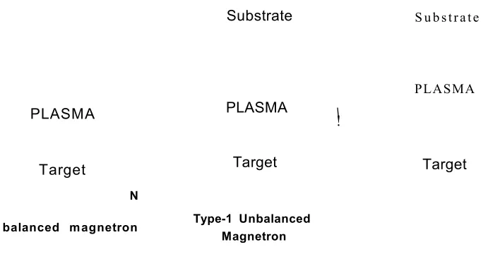
target. In 1986, Window and Sawides introduced the concept of unbalanced magnetron
sputtering which involves strengthening either the outer ring of magnets or inner pole
with respect to each other. This configuration pushed the plasma further towards the
substrate which is confined to the target in the case of balanced magnetron sputtering
[12-14]. Munz et al have reported that the substrate bias current density should be
2mAcm" or more for the reactive deposition of TiN [13] and it is possible with the
above said configuration. The difference in the plasma confinements observed for
balanced and unbalanced magnetic configurations is shown in Fig. 2.9.
Substrate S u b s trate
PLASMA
PLASMA
PLASMA \!
Target Target
Target
N
[image:32.612.112.466.351.531.2]Type-1 Unbalanced Magnetron balanced magnetron
Figure 2.9 Schematic representation of the plasma confinement observed in different magnetron sputtering sources adapted from Ref. [ 10]
Multiple cathode sputtering systems are quite useful in eliminating the
shadowing effect while depositing on complex components [16, 17]. In 1990, Sproul
and co-workers deposited TiN coatings in a multiple cathode opposed magnetron
sputtering system using two different magnetic configurations such as mirrored and
C H A R T E R A____________________________________________________________________________________________ L I T E R A T U R E R E V I E W poles face each other and opposite poles face each other in the closed filed (Fig. 2.10).
Cathode 1 Cathode 2 Cathode 1 Cathode 2
H
Substrate Substrate
N N
S
Field lines Field lines
b
Figure 2.10 Schematic representation of a) mirrored and b) closed field unbalanced magnetic configurations [15]
They have also reported that, for mirrored configuration, the substrate bias
current was very low since the plasma density is low at the substrate. A very high
substrate current was observed in the case of closed field setup. The sputtering pressure
also affects the substrate bias current. At high pressures, secondary electrons loose
considerable amount of energy due to the intense collisions near the targets before
arriving at the substrate. Hence the degree of ionization is very low which contributes to
lower substrate bias current. When the pressure is reduced, the vice-versa occurs and
more substrate bias current is generated. However, if the pressure is further dropped, a
decrease in substrate bias current is observed due to the fewer gas atoms available for
the collision despite having the secondary electrons with significant energy for
ionization. TiN coating deposited in the mirrored configuration exhibited poor adhesion
with voids due to low ion fluxes whereas the adhesion and hardness was relatively high
in the case of coatings made in closed field configuration since high flux ion
CHAPTER 2 LITERATURE REVIEW with multiple magnetrons in closed field configuration [19]. Moreover ionisation
efficiency in the plasma is improved by replacing first generation ferrite magnets with
stronger rare earth magnets. Rare earth magnets are capable of generating field strengths
in excess of lkG at the target surface whereas ferrite magnets could generate weak
magnetic field in the range between 300-500 G. Therefore, more ion current is seen at
the substrate with rare earth magnets [1 0, 2 0].
2.2.1.4 Pulsed Magnetron sputtering
The plasma density at the substrate for the deposition of good quality coatings
can be increased by increasing the target power density, besides exploiting the different
unbalanced magnetic configurations. Though the applied power is limited by the
thermal load on the targets, increasing the input power to the target is possible, provided
it is distributed over a larger target area. The pulsed magnetron sputtering technique
(over 20 kHz) can be used for this purpose [21]. AC (alternating current) or DC power
supply coupled with a pulsing unit is used for this purpose. However, the pulsed DC
sputtering is widely used. In 1991, Gruen have reported in his patent that the pulsed DC
sputtering can be utilized to generate the target power densities of less than 50 Wcm'
and the current density of 0.5 mAcm' at substrate by pulsed DC sputtering [22]. It has
been reported that the high bias current densities of up to 10 mA cm' 2 was observed
with TiN unipolar pulsed sputtering [21].
Pulsed DC sputtering can be exploited to overcome the problems due to the
'target poisoning' effect too. The 'target poisoning' is defined as the formation of a thin
layer of reacted 'compound film' on the target surface during dc reactive magnetron
sputtering. The different sputtering yield of the target material and compound film
affect the sputtering rate and stoichiometry of the deposited film which eventually leads
to the poor performance of the coatings. Moreover, if the film is an insulator like
CHAPTER 2 LITERATURE REVIEW in the form of an 'arc'. Due to this high current density arc discharges; droplets are
ejected from the target which can also cause defects in the growing film. And, the
damaged area may be prone to more arcs. Frequent arc discharges also lead to
[image:35.612.100.485.158.415.2]fluctuations in the process parameters which results in interrupted sputtering
[10, 21, 23]. The difficulties in sputtering of insulators were first reported by Wehner in
1955 [24].
100
-100
= o -200 >
E -300
400
-500
-600
Pulse-off
Pulse-on
H
I---50 100
Time, microseconds
l
150
Figure 2.11 Schematic representation of the target voltage waveform for a pulsed DC power supply operating in asymmetric bipolar pulse mode [1 0]
There are two types of pulsed DC sputtering: unipolar where only a single
magnetron is connected to a pulse power supply and bipolar where two magnetrons are
connected to the same power supply. In the unipolar sputtering, the voltage applied to a
single target is pulsed between the typical operating voltage (- 400 to 500 V) and
ground. The target material is sputtered off from the target during the pulse-on time and
then the discharging takes place during the pulse-off time. In the bipolar sputtering, the
polarity of the voltage applied to the target during 'pulse-on' time is reversed during the
CHARTER Z LITERATURE REVIEW neutralise the accumulated positive charge due highly mobile electrons in the plasma
than ions. This is called as 'asymmetric bipolar pulsed DC since the voltage applied to
the target is not fully reversed. In this case, the target material is sputtered off from the
target during the pulse-on time and, subsequently the positively charged target layer is
neutralized during the pulse-off time since the voltage becomes positive [10, 21, 23].
The RF sputtering can also be utilized to deposit the insulating films with
superior qualities. The plasma is ignited using RF generator (typically operating at
13.56 MHz) along with a matching network to maximise the power transmission from
the generator to the electrode. An alternating voltage is applied to the target. During the
negative half cycle, the target material is sputtered off from the target and, subsequently
the accumulated positive charge is neutralized during the positive half cycle. However,
the deposition rates are usually low since the sputtering takes place during only the
negative half cycle [10, 23]. RF deposition of insulating oxide films can be found
elsewhere in the literature [8, 25, 26].
2.2.1.5 High Power Impulse Magnetron Sputtering (HIPIMS)
HIPIMS is also a pulse power technology that utilizes much higher peak target
power density which results in a much higher ion current density at the substrate
compared to other magnetron sputtering techniques [13, 22]. The power density applied
on the target is increased by decreasing the duty cycle of the pulses. A typical HIPIMS
power supply used by Kouznetsov et al. in 1999 for the deposition of copper (Cu)
comprises a conventional DC power supply coupled with a pulsing unit as shown in
Fig. 2.12. The pulsing unit is a combination of a charging circuit and a trigger circuit.
The capacitor is charged and discharged via a thyristor switch by charging and trigger
L H A r 1LK Z LITLRATUKL KLVIcW
] anode
3 cathode Chargingcircuit Trigger
circuit
DC power supply
Figure 2.12 An electric circuit diagram representing a HIPIMS pulse generator with a pre-ionizer [28]
Kouznetsov et al. have utilised a peak power density of 2.8 kWcm’ and
observed a peak ion current density of 3.4 Acm 2 at the substrate during the deposition
of Cu. The typical voltage and current behaviour observed during this discharge is
shown in Fig. 2.13. The average power was kept to be less than 800 W to avoid
overheating the target. The plasma analysis using Langmuir probe showed that the
ionized flux arriving at the substrate comprised 70% of ionized copper. Moreover, a
dense coating without any voids was observed within the via-holes containing
negatively biased silicon substrates. This indicated the strong directionality of the
deposited ion flux which could be useful for various applications. Also, increased target
utilization was observed with considerably broader race track [27]. It is well known that
arc free operation is essential for a stable process and the deposition of high quality
coatings. A number of arc controlling devices have been built for dealing with the arcs
generated during conventional sputtering such as DC [29, 30]. In 2004, Christie et al.
demonstrated the successful operation of their power supply with arc handling for high
L H A r 1EKZ LITERATURE REVIEW
2 (XX)
5(X)
>
o
I (XX)
>
5(X)
2(X)
200
1 5 0 2 5 0
5 0 1(X)
0
Time (ps|
Figure 2.13 A typical voltage and time trace for the HIPIMS discharge [27]
Ehiasarian et al. observed up to two-fold ionised metal ions of Cr and Ti
(Cr1+,Cr2+ and Ti1+) while investigating the plasma composition using optical emission
spectroscopy (OES) during high power pulse sputtering of Cr and Ti. The Ti ion to
neutral spectral line ratio found to be increased a factor of 5 compared to RF coil
enhanced sputtering. The peak power applied to the target was 3 kWcm'2. The peak ion
current density also considerably increased with increasing peak target current. The
peak plasma density was of the order of 1013 Cm"3. The degree of ionisation of the
sputtered Cr flux was 30% [32], In 2004, Ehiasarian and Bugyi utilised a power supply
capable of delivering peak currents of up to 3000 A and at a voltage of 2000 V for the
sputtering of Ti in an industrial size sputtering machine. The power supply enabled with
the arc suppression design minimized the arc energy and facilitated arc free sputtering
for several hours [33].
The time evolution of the HIPIMS plasma was first reported by Macak et al. in
2000 [34] and later studied in detail by Ehiasarian et al. [32]. The comparison between
the discharge current trace and the optical emission spectra observed during the
sputtering of Ti in Ar atmosphere showed that the plasma was Ar dominated in the
CHAPTERZ LITERATURE REVIEW period of time [34]. This can be explained by the gas rarefaction effects discussed by
Rossnagel and Kaufman where the working gas density in front of the target was found
to be decreased due to the transfer of the kinetic energy of the sputtered atoms to the gas
when the discharge current to the target was increased [35].
Usually the deposition rate by HIPIMS process is found to be lower compared to
a conventional DC magnetron sputtering at the same average power. Several studies
have reported on the lower deposition rate. The most important reason for the lower
deposition rate is that some of the newly generated metal ions in the sputtered material
close to the target are attracted back to the target surface by the cathode potential. The
metal ions that return to the target causes sputtering called 'self-sputtering' (sputtering of
target material by target material ions) [28, 36, 37]. Christie et al. have demonstrated by
their model that it is possible to achieve increased deposition rates in HIPMS discharge
compared to conventional DC magnetron sputtering provided the self-sputtering yield
exceeds the process gas ion sputtering yield by unity or more [36]. The various other
factors affecting the deposition rates in HIPIMS process can be found
elsewhere [28, 37].
2.2.1.5.1 Surface pre-treatment using HIPIMS discharge
A surface pre-treatment is performed to remove the contaminants prior to
coating deposition during the PVD processes. The substrate is sputter cleaned by
bombardment of Ar ions generated in Ar glow discharge plasma. The Ar ions are
accelerated to several hundred eV by applying a huge negative bias voltage on the
substrates. However, sputter cleaning by gas ions has few disadvantages such as the
difficulty in removing carbon-based contaminants and the incorporation of the gas ions
into the substrate. The incorporated gas ions induce increased strains in the substrate
CHARTERL LITERATURE REVIEW substrate cleaning. The plasma density enhancement can be achieved by increasing the
pressure and/or by using RF or mid-frequency bipolar pulsing discharge. However, the
complex nature of RF discharge systems may lead to reproducibility issues. Cathodic
vacuum arc etching can also be used for the surface pre-treatment since it is possible to
i n o
generate high plasma densities of 1 0 cm' and ion current densities of up to
10 mA cm' at the substrate by this technique. The plasma generated in such discharge
is found to have highly ionized metal flux and even the discharge may be operated
without any process gas. The metal ions accelerated by suitable substrate bias can be
used for the substrate cleaning since the high energy ion bombardment may lead to
significant resputtering whereas the low energy ion irradiation cause metal deposition
instead of sputter cleaning [38]. Schonjahn et al. have reported that the Cr ion
irradiation on steel substrate using steered cathodic arc discharge resulted in a Cr
implanted interface zone which promotes localized epitaxial growth of the coating over
individual grains of the substrate [39]. However, cathodic arc discharges are
characterized to produce droplets which are undesirable for many applications. The
mechanism behind the formation of the droplets, their role on the microstructure
evolution during thin film deposition and subsequent effect on certain properties is
discussed in detail in other sections.
HIPIMS can also be used for the substrate pre-treatment as it also produces
highly ionized metal flux comparable to an arc discharge. In addition, the HIPIMS
discharge is free of the macro particles. Typically, a high substrate bias voltage of
greater than 1000 V is used for HIPIMS etching. Ehiasarian et al. have observed the Cr
ion implantation in the stain less steel substrates (substrate bias - 1 2 0 0 V) when
subjected to Cr ion irradiation by HIPIMS discharge. Moreover the CrN coating
deposited after the Cr ion pre-treatment exhibited superior adhesion with enhanced
CHAPTER 2 LITERATURE REVIEW columnar, dense and free of droplets [40]. Further studies on the adhesion strength of
CrN coatings showed that the coatings deposited after HIPIMS pre-treatment exhibited
superior adhesion in comparison to pre-treatments in Ar glow discharge and cathodic
vacuum arc processes. Also, the interface was found to be free of amorphous native
oxides; hence a well-defined crystal structure at the coating - substrate interface which
promotes the localized epitaxial growth of the coating [38].
2.3 Cathodic arc deposition
Cathodic arc deposition technique is one of the oldest deposition techniques and
dates back to the 18th century. Edsion was first to patent the practical applications of
cathodic arc coatings [41]. Cathodic vacuum arc can be defined as a high current, low
voltage electrical discharge between two electrodes by means of highly ionized plasma
of vaporized electrode material generated by the arc itself in a vacuum environment.
The plasma is generated locally at one or several tiny mobile locations called 'cathode
spots' on the cathode in which most of the basic processes of the arc take place [42, 43].
Cathode spots are originated at micro-protrusions on the surface of the cathode. Arc
discharges are characterised with low voltages in the range between 20 and 60 V. Also,
the discharge voltage is influenced by the cathode material and the magnetic field
strength. The applied potential can be multiplied by up to 5 orders of magnitude due to
the whisker-like geometry of the micro-protrusions. In addition, the electric field can
attain values of 105 Vm' 1 [44]. This electric field in combination with sufficient current
density yielded at micro-protrusions is enough to cause Joule heating in the emission
regions which eventually prompts the rapid 'explosion' of the cathode material,
ionisation and electrical breakdown. The plasma and current density in the vicinity of
CHAPTER 2 LITERATURE REVIEW velocities of about 1 0 ms' due to the highly energetic metal ions typically with kinetic
energies of 50 -150 eV and the very high pressure gradient near the cathode [41, 43].
Figure 2.14 Basic arc evaporation processes and potential distribution adapted from Martin et al. [46]
Fig. 2.14 shows schematic of typical arc evaporation processes including the
potential distribution between the electrodes. The vaporized flux comprises substantial
amount of droplets or macro particles (typically few nm - micron size) of the cathode
material. The droplets are ejected during the explosive emission of micro-protrusions in
the cathode spot from the molten material which is not sufficiently heated to sublimate.
It has been reported that materials have low melting point produce more and larger
macro particles and they are likely to move along straight line trajectories [28, 41]. The
macro particles are then embedded in the growing coating during the thin film
deposition in cathodic vacuum arc discharge. These embedded droplets then create
porosity by shadowing the deposition flux and nucleating large scale growth defects
throughout the thickness of the coating [47]. These defects contribute in deteriorating
the performance of the coatings. Wang et al. proved that the droplets accelerated the
substrate corrosion by corroding concurrently with the localised galvanic corrosion of
the substrate [48].
-fr ANODE
ION FLUX
Q ^ ~ PHOTONS
J) WE ION CLOUD
EVAPORATION VAPOR
M A CRO / PARTICLES VOLTS
CHAPTER Z LITERATURE REVIEW The emission of the macro particles can be minimized by introduction of
magnetic fields in the region near to the cathode. Furthermore, a drastic reduction of
droplets in the coating is possible by guiding the plasma with magnetic filters. The
plasma is steered away from the cathode to the substrate which is not in line of sight, by
the combination of magnetic and electric fields generated by the magnetic filters [41].
A magnetic filter made of permanent magnet proposed by Ramalingam et al. can be
seen in Ref. [49]. Various designs of filter have been proposed several researchers [50].
However, it has been reported that the up-scalability of many filters is not easy due to
geometry of such filters [28].
2.4 Microstructure evolution during coating growth
Polycrystalline thin films prepared by various techniques demonstrate a vast
variety of microstructures characterized in terms of grain size and crystallographic
orientation, lattice defects, phase composition and surface morphology. It is well
known that the growth of thin films deposited by PVD techniques includes the
following consecutive specific structure evolution stages: nucleation, formation of
island, coalescence of islands, growth of polycrystalline islands and channels,
development of continuous structure and thickness growth [51]. These processes are
illustrated in Fig. 2.15. The three basic mechanisms occurring during the above said
film forming processes are as follows [53]:
• The incident atoms become loosely bonded adatoms by transferring the kinetic
energy to the lattice
• Then the adatoms are desorbed, by evaporation or sputtering or more commonly
become trapped at low-energy lattice sites after exchanging energy with the
CHARTERZ LITERATURE REVIEW
Nucleation and growth
Thickening
E m _ m n
M M Hc d
Figure 2.15 Schematic of grain structure evolution during deposition of polycrystalline thin films [52]
The film forming processes such as surface diffusion, bulk diffusion and the
sublimation energy can be quantified in terms of the activation energies of surface and
bulk diffusion, and the sublimation energy. It has been reported that these energies are
proportional to the melting point for many pure metals. Hence several of the basic
processes that are responsible for the differences in the resultant coating structures can
be expected to dominate over different ranges of T (substrate temperature)/Tm (melting
point) [53].
Understanding the correlation between the microstructure evolution and process
parameters is essential since the former strongly determines the properties that translate
into the performance of a material. Various structure zone models based on the
experimental results have been proposed to classify the surface morphology of films
prepared by various techniques. The Movchan - Demchishin basic structure zone model
(Fig. 2.16) was based on the substrate temperature gradient maintained during the
deposition of Ti, Ni, W, ZrC>2, AI2O3 and Fe using electron beam evaporation. This
CHAPTER 2 LITERATURE REVIEW (0.5<T/Tm < 1). The zone 1 consisted of tapered crystals with dome tops (rough)
separated by voided column boundaries. The diameter of the crystals found to be
increased with T/Tm [53] which indicates very low activation energy and implies very
little surface diffusion. The zone 2 contained smooth columnar grains separated by well
defined, dense, intercrystalline boundaries. In this case, the width of the grains increased
with T/Tm and this could be attributed to the activation energy yielded that was
approximately equal to that for surface diffusion. The zone 3 was characterized with
equiaxed grains with a bright surface which could be due to an activation energy
corresponding to the bulk diffusion [53].
Z O N E 3
Z O N E 1 Z O N E 2
0 . 3 0 . 5
Substrate tem perature (T/Tm)
Figure 2.16 Movchan - Demchishin structure zone model [53]
2.4.1 Effect of sputtering parameters on microstructure evolution
In sputtering deposition, the process parameters such as substrate temperature,
sputtering gas pressure, substrate bias, etc. affect the microstructure. Thornton extended
the basic structure zone model to sputtering by considering the effect of the sputtering
gas. The proposed model was based on the experimental results of Ti, Cr, Fe, Cu, Mo
and Al alloy coatings deposited on metal and glass substrates using cylindrical-post and
hollow-cathode magnetron sputtering systems. The structure zone model for sputtered
C HA RTERI LITERATURE REVIEW
Figure 2.17 Thornton structure zone model [53]
I SO I AT [ 0 Z O N F 1 G R O W T H D E F F C T S
S H A D O W I N G P R O C F SSE S
S U B S T RATE Z O N E 1 S T R U C
i n d u c e d]
C T U R F
srz 7~--- *
S U R F A C E D I F F U S I O N P R O C F SSE S
BULK D I F F U S I O N P R O C E S S E S
C O M P O S I T E S T R U C T U R E D I AG R A M
•r^JZQNE
G A S I N D U C E Z O N E 1 S T R U C T U R E
i 2 > l Z O N E 3J\~r R E C R Y S T A L L I Z A T I O N
G R A I N G R O W T H
I NE RT G A S
P R F SSI JRF ( P a l 0. 15
0. 1
S U B S T R A T E T E M P E R A T U R E ( T / T m )
Figure 2.18 Schematic showing the superposition of physical processes that establishes structural zones [53]
The formation of pronounced (dome shaped rough tops) crystal structure with
open column boundaries in zone 1 is promoted by the substrate roughness, high argon
LH A rTER I LITERATURE REVIEW to low adatom mobility which is insufficient to diffuse through the open boundaries
formed by the atomic shadowing effect. The zone T (internal structure of zone 1) is
characterized by poorly defined fibrous crystals separated by dense boundaries at zero
T/Tm on infinitely smooth substrates.The zone T terminates at T/Tm ~ 0.3 for single
phase materials on smooth substrates. Interestingly, the fibrous zone T structure
transformed to rough zone 1 structure at high inert gas pressure and low T/Tm even on
smooth substrates due to low adatom mobility. However, the influence of inert gas on
coating growth at sufficiently elevated temperatures is found t
![Figure 2.11 Schematic representation of the target voltage waveform for a pulsed DC power supply operating in asymmetric bipolar pulse mode [ 1 0 ]](https://thumb-us.123doks.com/thumbv2/123dok_us/740134.578860/35.612.100.485.158.415/figure-schematic-representation-voltage-waveform-operating-asymmetric-bipolar.webp)