1086/
2086
Altos Computer Systems
1086/2086
Copyright Notice
Manual Copyright©1986 Altos Computer Systems Programs Copyright©1986 Altos Computer Systems All rights reserved. Printed in U.S.A.
Unless you request and receive written permission from Altos Computer Systems, you may not copy any part of this document or the software you received, except in the normal use of the software or to make a backup copy of each diskette you received.
Trademarks
The Altos logo, as it appears in this manual, is a registered trademark of Altos Computer Systems.
UNIX8 is a registered trademark of AT&T Bell Laboratories. UNIX System IIl'M is a trademark of AT&T Bell Laboratories. XENIX8 is a registered trademark of Microsoft Corporation. MULTIBUS8 is a registered trademark of Intel Corporation.
IBM8 is a registered trademark of International Business Machines Corporation.
PC/AT8 is a registered trademark of IBM Corporation.
System 34 Double Density (MFM)8 is a registered trademark of IBM Corporation.
Scotch8 is a registered trademark of 3M Corporation.
3279/SNA is an Altos Implementation of ACCESS/SNA developed by Communications Solutions, Inc.
WorkNet8 is a registered trademark of Altos Computer Systems.
Limitations
Neither Altos nor its suppliers make any warranty with respect to the accuracy of the information in this manual. Altos Computer Systems
reserves the right to make changes to the product described in this manual at any time and without notice.
FCC Warning
This equipment generates, uses, and can radiate radio frequency energy and if not installed and used in accordance with the instruction manual, may cause interference to radio communications. It has been tested and found to comply with the limits for a Class A computing device pursuant to
Subpart J of Part 15 of FCC Rules, which are designed to provide reasonable protection against such interference when operated in a commercial
environment. Operation of this equipment in a residential area is likely to cause interference in which case the user, at his own expense, will be required to take whatever measures may be required to correct the
ABOUT THIS MANUAL
This manual contains detailed service information for the technician who is trained in digital electronics, microcomputers, and operating systems.
The purpose of this manual is to describe the operation of the 1086/2086 Computer System and provide specific instructions to enable the technician to effectively service the 1086/2086.
Careful attention to the preventive and corrective maintenance information contained in this manual will
ensure maximum trouble-free operation from the Altos 1086/2086 Computer System.
This manual is organized into the following chapters:
Chapter 1 System OVerv i "
• describes the features and capabilities of the system
• provides a hardware overview of the major circuits and peripherals
• lists and shows the location of the field replaceable assemblies comprising the system
• describes and shows the dedicated and recommended expansion plug-in printed circuit board (PCB) locations
• describes and shows the locations of the front and rear-panel controls, connectors, and indicators
• discusses the software available for the system
Chapter 2 Specifications
About This Manual
• shows the overall physical dimensions of the' system
Chapter 3 Principles of Operation
• explains how the pI ug-in PCB subsystems inte,rface
to the system through the system bus
• describes how the system is initialized or programmed at power-up
• describes the programmed steps performed in the main operational sequences
• lists the addresses for each device that can be accessed
• includes bit definitions for the ports and external registers
• includes pertinent timing diagrams and general programmable array logic (PAL) information'
Chapter 4 Maintenance'
• includes 115/23rtJ VAC conversion instructions
• provides cleaning procedures
• provides removal and replacement procedures.
• provides shipping information
Chapter 5 Troubleshooting
• discusses troubleshooting aids and techniques
• includes detailed troubleshooting procedures using power-up, system-confidence, and field-service diagnostics
About This Manual
Appendices
Includes jumper pinning, loopback connector assembly, storage device specifications, and utility program information.
Glossary
Includes an alphabetical list and definitions of specialized terms and acronyms used in this manual.
Index
Includes an alphabetical list of names, subjects, or topics contained in this manual with the page numbers where they occur.
RELATED PUBLICATIONS
The following is a list of publications that contain additional information relating to the 1986/2986 system. The 1186/2186 OWner's Guide is shipped with the system. The remaining publications are optional and are divided into three types: (1) basic (run-time) system manuals that contain information for installing and using the operating system, (2) development system manuals that include reference and tutorial material
for programs available in the development system, (3) supplemental information manuals that are referenced in the text of this manual and contain additional
information required to understand the operation of the 1986/2986 system. The publications listed here are available through your Altos distributor or directly from integrated circuit manufacturers.
Shipped with 1086/2086
About This Manual
Basic System
• Installing XENIX on Your 1086/2086 System (Altos part no. 690-16630-XXX)
• Introduction to XENIX (Altos part no. 690-13449-XXX)
• Directory of XENIX Commands (Altos part no. 690-1664- XXX)
Development System
Altos Development System set (Altos part no. 583-13801-XXX)
Supplemental Information
• Altos 1086/2086 System Reference Manual (Altos part no. 690-15623-XXX)
• Altos 1086/2986 Illustrated Parts List (Altos part no. 699-15625-XXX)
• Altos 1086/2086 Remote Diagnostics Instructions (Altos part no. 690-17072-001)
• IEEE 796 System Bus Specification (Mu1tibus)
• Intel IAPX 286 programmer's Reference Manual
• Intel Microsystem Components Handbook
• Intel Microprocessor and peripheral Handbook
• Intel 8254 Data Book (Mode 2)
• National Semiconductor 58167 Applications Note Data Handbook
• Advanced Micro Devices 9517 Technical Reference Manual
• Zi10g Data Handbook/Technical Manual
About This Manual
• Hitachi HD68459 Data Book
• Hitachi Microcomputer Handbook
• National Cash Register 5385 SCSI Protocol Controller Data Sheet
• Archive QIC-92 1/4-Inch Tape Drive Interface Standard
• Archive QIC-24 1/4-Inch Cartridge Tape Drive Format Standard
• Archive QIC-36 Basic 1/4-Inch Cartridge Streaming Tape Drive Interface Standard
• NEC PD765 Data Sheet
• NEC Data Handbook
• ANSI X3T9.2/82-2 SCSI Small Computer System Interface
• National Cash Register Data Handbook
SPECIAL SYMBOLS AND NOTATIONS
About This Manual
Symbol/Notation * (Asterisk)
h
d
b
Description
Used following a capitalized mnemonic or signal name to
indicate a nnot n (complement) function or an active low signal.
Example: PERR*
Used after a number to
indicate that the number is a hexadecimal notation.
Example: 25h
Used after a number to
indicate that the number is a decimal notation.
Example: l6d
Used after a number to
indicate that the number is a binary notation.
Example: 0lb
About This Manual
•
• •
02000
j
'\ )
'\
TABLE OF CONTENTS
1 SYSTEM OVERViEW
SYSTEM DESCRIPTION • • • • • • • • • • • • 1-3 Characteristics • . • • • • • • • • • • • • 1-3 Architecture • • • • • • . • • • • • • • • 1-3 Configurations. • • • • • • • • • • • • • • 1-4 Networking. • • • • • • • • • • • • • • 1-4 Communications. • • • • • • • • 1-5 Diagnostics • • • • • • • • • • • • • • • • 1-5 Power-Up Tests • • • • • • • • • 1-6 User System-Confidence Tests • • • • 1-6 Field-Service Diagnostics. • • • • • • • 1-6 Hardware • • • • • • • • • • • • • • • • • 1-7 System Bus • • . • • • • • • • • • • • • 1-7 Central Processing Unit (CPU) PCB • • • 1-8 Memory PCB • • • • • • • • • • • • • 1-8 Communications PCB • • • • • • • • • 1-8 File Processor PCB • • • • • • • • • • • 1-9 Controller PCB • • • • • • • • • • • 1-1~ FIELD REPLACEABLE UNITS • • • • • • • • • 1-11 CONTROLS, CONNECTORS, AND INDICATORS • • • • • 1-12 Front Panel • • • • • • • • • • • • • • • • 1-13 Rear Panel • • • • • • • • • • • • • • 1-13 PLUG-IN PRINTED CIRCUIT BOARD,LOCATIONS. • 1-15 SYSTEM SOFTWARE. • • • • • • • • • • • • • • • 1-15 Operating System Programs • • • 1-15 Address Translation • • • • • • • • 1-17 Disk Performance • • • • • • • • • •.• • 1-17 Serial Port Performance. • • • • • • 1-17 Compatibility. • • • • • • • • • • • 1-17 Diagnostics. • • • • • • • • • • • • • • 1-18
2 SPECIFICATIONS
INTRODUCTION • • • • • • • • • • • ELECTRICAL SPECIFICATIONS. • • • ENViRONMENTAL SPECIFICATIONS • PHYSICAL SPECIFICATIONS. • ••
Table of Contents
3 PRINCIPLES OP OPERATION
INTRODUCTION • • • • • • • • • • • • • • • • • 3-5 BLOCK DIAGRAM DESCRIPTION. • • • • • • • • • • 3-5 System Bus. • • • • • • . • • • • • • • 3-5 Central processing unit (CPU) • • • 3-6 System Memory • • • • • • • • • • • • • 3-7 Communications. • • • • • • • • • • 3-7 File Processor • • • • • • • • • • • • • • • 3-8 Controller • • • . • • • • • • • • • • • • • 3-8 DETAILED CIRCUIT OPERATION • • 0 0 0 • 3-9
NOTE
For convenience, each of the following PCB subsystem descriptions have a red locator tab on the right edge of the first page.
System Bus Interface. • • • • 0 3-11
Bus Masters. • • • • • • • • • • • • • • 3-12 Bus Slaves • • • • • • • • • • • 3-12 Bus Signals. • • • • • • • • • • • • 3-12 Data Transfer Operations • • • • 3-16 Interrupt Operation. • • • • 3-18 Bus Exchange 0 • • • • • • • 3-19 Lock Operation • • • • • • • • • 3-20 Timing • • • • 0 • • • • • • 3-20 Central processing Unit (CPU) PCB • • • 3-27 CPU Initialization • • • • • • • • • • • 3-27 Microprocessor . • • • • • • • • • • 3-28 Microprocessor Address Decoder Logic • • 3-28 80286 Memory Map • • • . • • • • • • • • 3-28 Local Bus Control Logic. • • • • •• 3-29 Local Bus. • • . . • • • • • • • • • • 0 3-33 Calendar Clock • • • • • • • • • • • • • 3-35 Interrupt Controller • • • • • • . • • • 3-35 System Memory Accessing and Address
Translation • • • • • • • • • • • • • • 3-35 Tag and Translation RAM Control Logic. • 3-37 Cache Memory Organization. • • • • • ' 0 • 3-38
System Bus Arbiter and priority Encoding
Logic • • • • • • • • • • • • 0 • • • 0 3-41
Microprocessor Ready Generator • • • • • 3-42 Jumper Descriptions •• 0 • • 0 • • • 3-42
Timing Diagrams. • • • 0 • 0 • • • • 3-44
Table of Contents
Memory PCB. • • • • • • • • • • • • 3-55 System Bus Interface • • • • 3-55 Row/Column Address Decoder • • • • • 3-57 Memory Transceiver Control • • • • • • • 3-57 Memory Arbiter • • • • • • • • • • • 3-58 RAM Refresh • . • • • • • • • • • . • • • 3-58 Address Space Allocation • • • • • . 3-59 Timing Diagrams. • • • • • • • • 3-59 Communications (SIO) PCB. • • • . . • • 3-63 I/O Microprocessor • • . • • • • • • • . 3-63 Local Arbiter. • . • • • • • • • 3-63 System Bus Interface • • • • • . 3-64 Local Bus Controller • • • • • •• • 3-65 Local Bus Interface. • • • • • • • • • • 3-65 Local Bus Transceiver Controller 3-66 Local Memory • • • • • • • • • •• • 3-66 Local Memory Decoder • • • • • • • • 3-68 System Memory Page Register • • • • • • • 3-68 Accessing System Memory. • • •• • • 3-69 I/O Port Addressing. • • • •• . • • 3-79 DMA Controller • • • • • • • • • • • • • 3-75 DMA Synch/Refresh Controller • • • • • • 3-77 DMA Read/Write Controller. • •• 3-77 DMA Page Register. . •• • • • • • • 3-78 Serial I/O Ports • • • • • • • • • • 3-79 Network Channel. • • • • • • •• 3-82 SCC Recovery • • . • • • • • 3-83 Programming Precautions. • • • • • • 3-83 Counter/Input/Output • •• . • • • • 3-85 CIa Programming Notes. • • • • • • • 3-88 Interrupt Priorities • • • • • • •• 3-99 Jumper Selectable Options. • • • • • • • 3-92 I/O Connectors • • • • • • • • • • • • • 3-93 Timing Diagrams. • • • • • • • • • • 3-95 File Processor PCB. • • • . • • • • • • 3-195
Table of Contents
DMA Controller • • • • • • • • • • • • • 3-117 Ping-Pong Buffer • • • • • • • • • • • • 3-118 ping-Pong Buffer Control Logic • • • 3-129 Controller Interface • • • • • • • • • • 3-121 Controller PCB Read/Write Control Logic. 3-122 Printer Controller • • • • • • • • • • • 3-122 SCSI Controller. • • • • • • • • • • • • 3-124 File Processor Initial Program Load
(IPL) Process. • • • • • • • • • • 3-126 Timing Diagrams. • • . • • • . • • • 3-126 Controller PCB. • • • • • • • • • • 3-137 Controller Initialization • • • • • • • • 3-137 Hard Disk Controller • • • • • • • • • • 3-137 Floppy Disk Controller • • • • • • • 3-149 Tape Controller • • • • • • • • • • • . • 3-143
4 MAINTENANCE
INTRODUCTION • . • • • • • • • • • • • . • • • 4-3 SELECTING 115/238 VAC OPERATION • • . • • 4-3 PREVENTIVE MAINTENANCE • • • • • • • • 4-5 Cleaning. • . . • • • • • • • • 4-6 'Dust Filters. • • • • • • • • • • • 4-6 Tape Heads • • • • • • • • • • • 4-9 Floppy Disk Drive. • • • • • • • 4-11 Exterior • • • • • • • . • • • • • • 4-12 Interior • • • • • • • • • • • • • • 4-12 CORRECTIVE MAINTENANCE • • • • • • • • • • 4-13 Removal and Replacement • • • • • • • • 4-13 Removing the Front Panel • • • • • • • • 4-13 Removing the Side Panels • • • • • • • • 4-15 Removing the Tape Drive. • • • • • • • • 4-16 Replacing the Tape Drive • . • • • • • • 4-18 Removing the Floppy Drive. . • • • • • • 4-19 Replacing the Floppy Drive • • • • • 4-21 Removing the Hard Disk Drive • • • • • • 4-22 Replacing a Hard Disk Drive. • • • • • • 4-24 Removing the Plug-In Printed Circuit
Boards. • • • . . • • • • •
Removing the Main Power Supply • • Removing the Backplane PCB • • • • Removing the Low-Pass Filter PCB
• • 4-26 • 4-27 • • • 4-28
(Early Version Only) • • • • • • • • • • 4-38 Removing the LED PCB • • • • • • • • • • 4-31 Removing the Clock Battery • • • • • • • 4-31
Table of Contents
SHIPPING A FIELD REPLACEABLE UNIT. • • • • • • 4-35 packaging the System Unit • • • • • • • • • 4-35 packaging Storage Devices • • • • • • • 4-36 packaging Printed Circuit Boards • • • • • • 4-36
5 TROUBLESHOOTING
INTRODUCTION • • • • • • • • • • • • • 5-3 TROUBLESHOOTING AIDS • • • • • • • • • 5-3 System Overview • • • • • • • • • • • • 5-3 principles of Operation • • • • • • • • • • 5-4 Diagnostics • • • • • • • • • • • • • • 5-4 Diagrams. • • • • • • • • • • • • • • • 5-4 Field Replaceable Unit Locations.. • • 5-5 TROUBLESHOOTING CONSIDERATIONS • • • • • • • • 5-5 Handling Static-Sensitive Devices • • • • • 5-5 Soldering Techniques and Equipment. • • 5-6 Removing Integrated Circuits. • • • •• 5-7 TROUBLESHOOTING PROCEDURES • • • • • • • • 5-11
Low-level Tests • • • • • • • • • • • • • • 5-13 power-Up Tests. • • • • • • • • • • • • 5-15 System power-Up Sequence • • • • • • • • 5-17 Communications power-Up Tests.. • • 5-18 CPU Power-Up Tests • • • • • • • • • • • 5-19 File Processor and Controller Power-Up
Tests • • • • • • • • • • • • • • • • • 5-37 CPU and File Processor Communication • • 5-41 Interrupt Signals. • • • • • • • • • 5-41 Communication Protocol • • • • • • • 5-41 System-Conf idence Tests • • • • • • • • • • 5-43 Booting the SDX Disk • • • • • • • • • • 5-43 Field-Service Tests • • • • • • • • • • • • 5-47 SDX Field Service Menu • • • • • • • • • 5-47 CPU Test Menu. • • • • • • • • • 5-52 File Processor and Controller Board Test
Menu. • • • • • • • • • • • • • • • 5-56 SIO Test Menu. • • • • • • • • • • • 5-61 File Processor and Controller PCB
Circuit Level Test Menu • • • • • • • • 5-67 Debugger Tests. • • • • • • • • • • • • • • 5-89 CPU Debugger Commands. • • • • • • • • • 5-89 Communications Debugger Commands
(Software Mode) • • • • • • • • • • • • 5-97 Communciations Debugger Commands
Table of Contents
APPENDICES
A JUMPERING
INTRODUCTION • • • • • • • • • MEMORY PCB JUMPERING • • • • COMMUNICATIONS PCB JUMPERING •
B S~RAGE DEVICE SPECIFICATIONS
. • . . . . • . A-3 . . . A-3 . . . • . . . . A-12
INTRODUCTION • • • • • • • • • • • • • • • • • B-3 CARTRIDGE TAPE DRIVE • • • • • • • • • • • • • B-3 Electrical Specifications • • • • • • • B-3 FLOPPY DISK DRIVE. • • • • • • • • • • • • • • B-4 Electrical Specifications • • • • • • • • • B-4 HARD DISK DRIVE. • • • • • • • • • • • • • • • B-5 Electrical Specifications • • • • • • • • • B-6
C UTILITY PROGRAMS
INTRODUCTION • • • • • • • • • • • • • • • C-3 BOOTING '!HE SDX DISK • • • • • • • • • C-3 FLOPPY FORMAT. • • • • • • • • • • • • • • • • C-6 FLOPPY COPY. • • • • • • • • • • • • • • • C-8 WORKING WITH HARD DISK BAD SECTORS • • • • • • C-l2
Terminology • • • • • • • • • • • • • • • • C-l2 Determining the Drive Number • • • • • • • • C-l4 DISPLAY HARD DISK CONFIGURATION TABLE. • • • • C-l4 SCAN HARD DISK FOR BAD SECTORS • • • • • • • • C-l6 FLAG HARD DISK BAD SECTORS • • • • • • • • • • C-l9 Drive Serial Number • • • • • • • • • • • • C-29 Entry Mode. • • • • • • • • • • • • • • • • C-29 Unflagging a Bad Sector • • • • • • • • • • C-24 HARD DISK FORMAT. • • • • • • • • I • • • • C-24
RECONFIGURE HARD DRIVE • • • • • • • • • • • • C-26
D LOOPBACK CONNECTORS
INTRODUCTION • • • • • • • • • • • • • \. • • • D-3
Table of Contents
E ADJOSTIlENT PROCEDURES
TAPE PHASE LOCK LOOP ADJUSTMENT.
. .
.
.
.
.
.
E-lGLOSSARY.
.
.
. . .
.
.
.
.
. . .
.
.
. . . .
G-lINDEX • •
.
. .
.
.
.
. . .
.
.
.
. . .
.
.
.
I-IList of Illustrations Figure Title
1-1 Field Replaceable Units • • • • • • • 1-12 1-2 Controls, Connectors, and Indicators • 1-14 1-3 Recommended Plug-In PCB Locations. • • 1-16
2-1 Maximum Overall Dimensions • •
.
.
.
• 2-9 3-1 81iJ286 Memory Map • • • • • • • • • 3-31iJ 3-2 Cache Memory Organization. • • • • • • 3-38 3-3 Cache Memory Search. • • • • • • • 3-41iJ 3-4 CPU PCB Timing Diagrams.. • • • • 3-44 3-5 Memory PCB Timing Diagrams • • • • • • 3-61iJ 3-6 Local Memory Map • • • • • • • • • • • 3-67 3-7 System Memory Page Register. • • • • • 3-69 3-8 Local I/O Map • • • • • • • • • • • • • 3-71 3-9 DMA page Register Block Diagram • • • • 3-78 3-11iJ Communications PCB Timing Diagrams • • 3-95 3-11 81iJ86 Memory Address Map. • • • • • • • 3-l1iJ8 3-12 81iJ86 System Memory Addressing. • • • • 3-l1iJ84-1 Il5/231iJ VAC Selection (Main Power
Supply) • • • • • • • • • • • • • • • 4-4 4-2 Il5/231iJ VAC Selection (Hard Disk
Drive) • • • • • • • • • • • • • • • • 4-5 4-3 Removing/Replacing the Front Panel
Table of Contents
Figure Title
4-8 Locking/Unlocking the Tape Drive
Mounting Screw. •
·
•· · ·
·
·
4-16 4-9 Removing/Replacing the Tape Drive.·
·
4-17 4-HJ Locking/Unlocking the Floppy DriveMounting Screw.
·
·
•·
•· · · ·
·
·
4-19 4-11 Removing/Replacing the Floppy Drive.·
4-29 4-12 Removing/Replacing the Hard DiskAC Connector.
· ·
·
·
· ·
· ·
·
· ·
·
4-23 4-13 Unlocking/Locking the Hard Disk DriveMounting Screws
·
·
· · · ·
•· ·
4-24 4-14 Removing/Replacing the PI ug-In PCBs. • 4-26 4-15 Removing/Replacing the Main PowerSupply.
· ·
·
· ·
•· · ·
·
•· ·
•·
4-28 4-16 Removing/Replacing the Backplane·
·
·
4-29 4-17 Removing/Replacing the Clock Battery·
4-32 4-18 Cable Interconnections· · · ·
•·
•·
4-33 5-1 Removing ICs (Cut pin Method).· · · ·
5-8 5-2 Removing IC Pins·
·
·
· ·
·
· · ·
5-9 5-3 Removing Solder from Plated-ThroughHoles
. · · ·
•·
•·
•·
•·
• • •·
5-19 5-4 Removing Solder from Lead ConnectionPads.
. ·
• • • •· · ·
• •· ·
• •·
5-11 5-5 System Power-Up Test Sequence BlockDiagram
· · ·
,; •· · ·
5-16 A-I Memory PCB Jumper-Pin Connectors· ·
·
A-4 A-2 Jumpers for One 1M Byte Memory PCB· ·
A-5 A-3 Jumpers for Two 1M Byte Memory PCBs. • A-5 A-4 Jumpers for One 2M Byte Memory PCB· ·
A-6 A-5 Jumpers for 2M and 1M ByteMemory PCBs
·
•·
·
•· ·
•· ·
•· ·
A-6 A-6 Jumpers for Two 2M Byte Memory PCBs. • A-7 A-7 Jumpers for Three 2M Byte Memory PCBs. A-7 A-8 Jumpers for One 4M Byte Memory PCB· ·
A-8 A-9 Jumpers for 4M and 1M ByteMemory PCBs
· · ·
• •· · ·
·
A-8 A-19 Jumpers for 4M and 2M ByteMemory PCBs
·
•·
•· · ·
•· · ·
A-9 A-II Jumpers for 4M, 2M, and 1M ByteMemory PCBs
· ·
· · · ·
·
·
· · ·
A-9 A-12 Jumpers for Two 4M Byte Memory PCBs.·
A-19 A-13 Reference Jumpers for 1M ByteMemory PCBs
·
•· ·
•·
•· · ·
• A-19Table of Contents
Figure Title
A-I4 A-IS A-16 A-17 A-I8 A-19 A-20 C-l
Reference Jumpers for 2M Byte Memory PCBs • • • • • • • • • Reference Jumpers for 4M Byte
Memory PCBs • • • • • • • • • Jumpers for SIO Communications (Factory Setting) • • • • • • Jumpers for SIO Communications COMM" • • • • • • • • • • • Jumpers for SIO Communications
COMM 1 • • • • • • • • • • • Jumpers for SIO Communications
COMM 2 • • • • • • • • • • • Jumpers for SIO Communications
COMM 3 • • • • • • • • • • • Hard-Disk Terminology. • • • •
·
.
.
• A-II· .
.
• A-II A-13 PCBs·
.
·
.
·
.
• • A-IS A-16 • •
• • A-17 A-18
· .
.
.
·
.
.
• C-12 D-l Parallel Printer Port LoopbackConnector • • • • • • • • • • • • • • D-3 D-2 Serial Communications (SIO) Loopback
Connector • • • • • • • • • • • • • • D-4 E-l Channel A and B Waveforms. • • • • • • E-2 E-2 Channel B Waveform • • • • • • • • • • E-3 E-3 Jumper and Test Point Locations
(Controller PCB). • • • • • • • • • • E-4
List of Tab! es Table 2-1 2-2 2-3 3-1 3-2 3-3 3-4 3-5 3-6 3-7 3-8 3-9 Title
Table of Contents Table 3-lIiJ 3-11 3-12 3-13 3-14 3-15 3-16 3-17 3-18 3-19 3-20 3-21 3-22 3-23 3-24 3-25 3-26 3-27 3-28 3-29 3-30 3-31 5-1 5-2 5-3 Title
Asynchronous-Channel Handshake Lines • 3-81 Synchronous-Channel Handshake Lines. • 3-82 CIa Port Descriptions. • • • • • • • • 3-86 Interrupt Daisy Chain. • • • • • • • • 3-90 Jumper Descriptions. • • • • • • • • • 3-92 Connector/Controller Configuration • • 3-93 Connector Pin Assignments. • • • • • • 3-94 Control and Status Port Assignments. . 3-110 , Control and Status Bit Assignments • • 3-110 Nonmaskable Interrupts • • • • • • • • 3-113 Interrupt controller Port Assignments. 3-114 Maskable Interrupts. • • • • • • • • • 3-114 DMA Controller Port Assignments. • • • 3-118 Printer Port Assignments • • • • • • • 3-123 Printer Status Port Bit Assignments. • 3-123 SCSI Controller Port Assignments • • • 3-126 Hard Disk Controller Port Assignments. 3-138 Hard Disk Controller Bit Assignments • 3-139 Floppy Disk Controller Port
Assignments • • • • • • • • • • • • • 3-141 Floppy Disk Control-Register Bit
Assignments • • • • • • • • • • • • • 3-141 Tape-Controller Port Assignments • • • 3-143 Tape-Controller Bit Assignments. • • • 3-144 Low-Level Trouble Analysis • • • • 5-13 Power Supply DC Voltages • • • • • • • 5-14 CPU Failure Status at Output Latch
Port. • • • • • • • • • • •
.
. .
•• 5-82 5-4 Hard Disk Controller ErrorRegister Bit Descriptions • • • • • • 5-28 5-5 Hard Disk Controller Status
Register Bit Descriptions • • • • • • 5-29 5-6 Floppy Disk Controller Status
Register 0 Bit Descriptions • • • • • 5-32 5-7 Floppy Disk Controller Status
Register 1 Bit Descriptions • • • • • 5-33 5-8 Floppy Disk Controller Status
Register 2 Bit Descriptions • • • • • 5-35 5-9 Floppy Disk Controller Status
Register 3 Bit Descriptions • • • • • 5-36 5-10 SDX Trouble Analysis • • • • • • • • • 5-72 A-I SIO PCB Jumper Descriptions. • A-12
Table
B-1
B-2
B-3
B-4
B-5
Table of Contents
Title
Cartridge Tape Drive Specifications. • B-4 Floppy Disk Drive Specfications. • • • B-5 5BM Byte Hard Disk Drive
Specifications. • • • • • • • • • • • B-6 8BM Byte Hard Disk Drive
Specifications. • • • • • • •
19BM Byte Hard Disk Drive
.
.
B-5CHAPTER
1
SYSTEM OVERVIEW
System Overview
SYSTEM DESCRIPTION
The Altos lB86/2B86 Computer System is a floor-standing computer designed for general processing, office
automation, and network fileserver applications. The system contains a CPU, system memory, I/O connections, mass storage, streaming tape backup, and a floppy disk drive.
Characteristics
The following are some of the main characteristics of the IB86/2B86:
• exceptional modularity for easy system expansion
• 8 MHz Intel 8B286 main microprocessor
• optional high-speed Intel 8B287 floating-point processor
• up to 451M bytes of formatted internal hard disk storage
• up to 8M bytes of RAM system memory
• 6BM byte streaming cartridge tape drive
• storage expansion beyond 45lM bytes via a small computer system interface (SCSI) channel. (-BB2 version of file processor subsystem only.)
• high-speed 32-bit expanded Multibus[tm]
• remote diagnostics (with optional modem) for rapid fault isolation to field replaceable units
Architecture
System Overview
The cartridge tape, floppy disk, and hard disk drive mass storage subassemblies are easily installed or
replaced by removing the front panel and sliding the subassemblies in or out of the chassis. The three available hard disk drive subassemblies plug directly into the backplane.
The system can contain up to eight plug-in PCB
subsystems (five PCBs are used for a minimum 19-user system) and five magnetic media storage subassemblies. All of the plug-in PCBs slide into the back of the
chassis and connect to the system backplane PCB located in the center of the chassis. The mass storage
subassemblies slide into the front of the chassis and also connect to the backplane PCB. The backplane PCB serves as the medium for data interchange between the processors, system memory, and mass storage
subassembl ies.
Configurations
The 1986/2986 system can be configured in a variety of ways. The smallest possible configuration (or minimum system) could be made with 1M byte of random access memory (RAM), 19 RS-232 ports, a 59M byte hard disk
drive, and a 1.6M byte floppy disk drive. More system memory, hard disk capacity, and RS-232 ports can be
added.
A larger system configured to support 29 or 39 users could contain a 2M byte or 4M byte memory PCB, two or three 19-port communications PCBs, a 199M byte hard disk drive, a 1.6M byte floppy disk drive, and a 69M byte cartridge streaming tape drive.
Networking
The 1986/2986 hardware supports local area networking (LAN). The networking hardware runs at two speeds: 759K and 1.4M bits per second. The slower speed allows the 1986/2986 to talk to Altos l86~ 486, 586/586T, and 986/986T networks. The higher speed allows the
1986/2986 to talk to other 1986/2986 systems. A simple low-cost, twisted-pair, RS-422 interface is used at the hardware level.
System Overview
The 108612086 uses the same type of WorkNet software that runs on most Altos systems. The WorkNet software allows transparent remote file access and remote
processor execution.
Communications
The 1086/2086 system supports several serial
communications protocols which are down-loaded to the serial communications PCB. These communications
protocols are run by the 8086 microprocessor on the communications PCB, which removes this burden from the main
cpu.
By using multiple communications PCBs,multiple communications protocols can be run at the same time. The software for running the communications protocols is downloaded into the RAM on the
communications PCB.
The software for 3270, 3780, X.25, and SNA protocols will run on the 1086/2086. The system is capable of supporting asynchronous modems for dial-up data base services or offsite communications and bisynchronous modems for IBM 3780 emulation. WorkNet can also be
supported through one port via a software command
communicating at 1.4M bits per second or 750K bits per second (used to connect compatibles to Altos
processors). The optional communications PCB
subsystem, configured with 32K bytes of RAM, supports certified X.25 or IBM/SNA software protocols.
Diagnostics
The 1086/2086 performs three major categories of
diagnostic tests. The first category is the built-in hardware tests contained in the power-up monitor
program. (Refer to System Software in this chapter for additional diagnostics information.)
The second category of tests is the user system-confidence tests. The final category is the field-service diagnostics (SDX) tests which can be run
System Overview
Power-Up Tests
The power-up tests are ROM-based and reside on the CPU, communications, and file processor PCBs. These
power-up tests are always performed when power is applied to the system to check the minimum hardware configuration on its particular PCB, identify any missing or failed assemblies, and then confirm com-munication with the system. These tests are always performed on power-up.
The CPU power-up tests include programmable read-only memory (PROM), cache memory, translation and tag RAM memory, clock, floating-point numeric processor,
interrupt, and system bus checks. The file processor power-up tests include local RAM and PROM, interval timer, system bus, DMA controller, and magnetic media controller checks. The communications PCB power-up tests consist of local RAM and PROM, I/O integrated circuits, DMA controller, interrupt, and system bus checks.
User System-Confidence Tests
The user system-confidence tests allow a system user to test the functionality of the system. These tests are menu driven. A full set of tests can be run with only one or two keystrokes on the system console. More detailed and flexible tests are also available for the service technician. A full set of system utilities for handling system configuration and mass storage devices is incl uded.
Field Service Diagnostics
The field-service diagnostics can be run either from the SDX floppy disk supplied with the system or from a remote service depot through the optional communi-cations modem. The principle advantage of the remot'e method of performing diagnostics is that only one PCB
(one of the communications PCBs) needs to be working in order to begin testing. In most multi-board systems, the CPU PCB, system memory PCB, controller PCB, and communications PCB must be working before diagnostic testing can start.
System Overview
In the lB86/2B86, the communications (SID) PCB contains a full l6-bit microprocessor that acts as a diagnostic controller on the system bus.
Thus, each PCB can be called up and tested separately, or the full system can be enabled and exercised to isolate and identify failures for repair or
replacement.
Another advantage of the remote diagnostic method is that the tests are run by highly trained technicians at the main Altos facility or at designated service
centers. The full expertise of Altos is available on the spot to evaluate a problem without waiting for a service technician to arrive.
The remote facility can call up specific PCB monitors or debuggers, or transmit the latest circuit-level diagnostics, with no interaction required from the user. The failed unit can, upon isolation, be easily replaced by the user or by the system administrator.
Hardware
The system hardware is partitioned so that each major function is performed by a single PCB. The five
required PCBs for the minimum lB-user system are the CPU, system memory, communications, file processor, and controller. All of these PCBs, except the controller, connect to the 32-bit system bus. Refer to Chapter 3 for a description of the system hardware operation.
System Bus
System Overview
Central Processing Unit (CPU) PCB
The CPU PCB contains an 8e286 microprocessor (running at 8 MHz,), an interrupt controller, and a calendar clock with battery backup.
Also available on the -ee2 version of the CPU PCB is an optional 8e287 floating-point numeric processor. The 8e286 is aided by a 4K byte instruction and data cache memory. When operating out of cache memory, the 8e286
runs with zero wait states.
When a memory write on the system bus occurs, the cache control hardware searches the cache. If there is a cache hit, then that location in the cache is marked as invalid. This feature of the cache makes it fully
coherent with system memory at all times. The cache hit rate has been measured at 88%, under typical use env ironments.
The CPU PCB contains memory mapping hardware that
splits up system memory into 4K byte pages to speed up task switching and prevent memory fragmentation
problems.
Memory PCB
The memory PCB comes in three sizes: 1M, 2M, or 4M bytes. The system memory is organized into long words of 32 bits and memory transfers can be made in 8, 16, or 32-bit quantities.
The memory PCB uses lSe nanosecond dynamic RAM inte-grated circuits (ICs) and features a typical access time of 24e nanoseconds with a typical cycle time of 4ee nanoseconds .Mul tiple memory PCBs can be installed in the le86/2e86 system.
Communications PCB
The communications PCB handles all of the serial communications for the le86/2e86 system and supports asynchronous and synchronous RS-232, and RS-422 network communi ca tions.
System Overview
The communications PCB supports up to 10 asynchronous ports1 three of which can be software-switchable to support two synchronous channels and one networking port.
The operating software for the communications proces-sor is down-loaded at boot time so that the communica-tions PCB becomes fully programmable.
The networking port is fully compatible with Altos B00K
bit WorkNet, 186, 486, 586, and 986 systems and can run at a faster 1.4M bit per second rate when communicating with other 1086/2086 and Altos 3068 systems. Several synchronous communications packages, which include the
X.25 and SNA protocols, are available to run on the
communications PCB. An Intel 8086 microprocessor (running at 8 MHz,) manages all the data flow, I/O interrupts, DMA channels, and communications with the CPU.
File Processor PCB
The file processor PCB manages the data flow to/from the Centronics parallel port and all of the mass storage devices in the system. The mass storage devices include the floppy disk, hard disk, and cartridge streaming tape drives, and all the peripherals connected to the SCS I channel.
NOTE
The -001 version of the file processor PCB
does not support small computer system
interface (SCSI) operation. The -002 version of the file processor PCB includes SCSI.
Some of the main characteristics of the file processor are:
• supports up to three internal hard disk drives and additional drives connected via the SCSI channel
System Overview
• concurrent transfer of the printer, tape, floppy disk, and hard disk data (only one hard disk at a time)
• performs overlapped seeks when more than one disk drive is connected
• performs reads and writes to consecutive sectors on the hard disk, even though data may be
scattered in system memory.
Controller PCB
The controller PCB contains the device controllers for the floppy disk, hard disk, and streaming tape drives. All of these device controllers take commands from the file processor.
The hard disk controller accommodates disk drives with ST506 or ST412HP interfaces and can handle data
transfer rates up to 5M bits per second. The hard disk controller can support up to three internal hard disk drives.
The tape controller can interface with Altos cartridge streaming tape drives with the QIC-36 interface and uses the QIC-24 format for putting data on the tape. The tape streams at 90 inches per second and has a maximum capacity of 60M bytes.
The floppy disk controller interfaces with a dual-speed floppy disk drive which uses either normal or high
capacity disks. The normal disks are fully compatible with the floppy disks used on the Altos 186, 486, and 586 systems.
System Overview
FIELD REPLACEABLE UNITS
The 1086/2086 Computer System contains the following field replaceable units (FRUS) (see Figure 1-1):
•
main power supply•
streaming tape drive•
hard disk drive•
floppy disk drive•
central processing unit (CPU) PCB•
memory PCB•
communi ca ti ons PCB•
file processor PCB•
controller PCB•
backplane PCB•
light-emitting diode (LED) PCBSystem Overview
MAIN POWER _ _ _ _ SUPPLY
BACKPLANE PCB _ _ ... CARTRIDGE
TAPE DRIVE
FLOPPY DISK_-I\Il~
DRIVE LED PCB
HARD DISK - - - + t ! .. " " DRIVE
PLUG·IN PCBs
(SEE PLUG·IN PRINTED CIRCUIT BOARD LOCATIONS)
LOW·PASS FILTER PCB (EARLY VERSION ONLY)
01311
Figure 1-1. Field Replaceable Onits
CONTROLS, CONNECTORS, AND INDICATORS
Refer to Figure 1-2 for the locations of the front and rear-panel controls, connectors, and indicators. The following is a description of the controls, connectors, and indicators indexed to the numbers in Figure 1-2:
[image:35.612.125.515.85.512.2]System Overview
Front Panel
1 RESET/ROB Switch. Key-operated switch that resets (boots) the system when turned to RESET and back to RUN. Allows normal system operation when set to RUN. If the key is turned to RESET and re-moved, the system will remain in the reset con-dition and will not operate.
2 POWER Indicator. Green light-emitting diode (LED) indicator that lights when power is applied to the system (rear panel POWER switch is in the on
position) •
3 DD 1, DD 2, and BD 3. Yellow LED indicators that light to indicate which hard disk drive is
selected.
Rear Panel
4 POWER Switch. Rocker switch that applies power to the system when placed in the on position (green LED indicator 2 on the front panel is lit). The system will boot when the POWER switch is placed in the off, then on, position while the RESET/RUN switch 1 on the front panel is in the RUN
position.
S Fuse Bolder. Holder that contains the main line-voltage fuse (Refer to Chapter 2 for the proper fuse rating).
6 AC IBPOT Connector. Three pin AC connector for attaching an AC power cord to the system.
7 DPS Jack. Jack for connecting a power fail status signal from an external uninterruptable power
source device to the system.
System Overview
9 Serial I/O Ports. Ports 0 through 9 on the com-munications PCB provide 10 asynchronous RS-232 ports for connecting terminals or printers to the system. Refer to the communications PCB descrip-tion in Chapter 3 for details on the serial I/O port capabilities.
rr
lieJIIEiI I~ 1
IIIl!1Io J III 111f II
~991
IIe
2e e, e,
3
~
T
~02002
Figure 1-2. Controls, Connectors, and Indicators
[image:37.612.125.516.92.670.2]System Overview
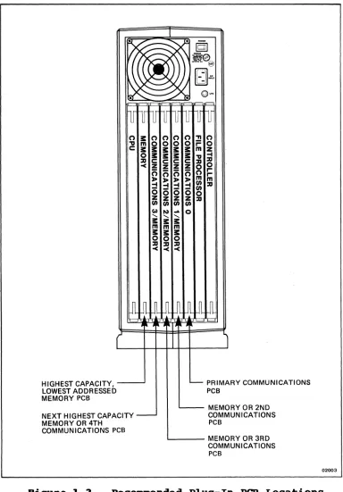
PLUG-IN PRINTED CIRCUIT BOARD LOCATIONS
The CPU, file processor, and controller PCBs are
dedicated to slots A, G, and B respectively in the back of the 1986/2986. The remaining slots, B through F,
are electrically identical which allows memory and communications PCBs to be installed in any order in these five slots. However, software requires that the memory and communications PCBs be jumpered according to
their logical assignment in the system (see jumper description information in Chapter 3 and Appendix A).
SYSTEM SOFTWARE
The system software supplied with the 1986/2986 consists of the operating system, utility, and diagnostic programs.
Operating System Program
The 1986/2986 Computer System is specifically designed for the XENIX 3.2 operating system.
The XENIX operating system supports the following development tools and programming ,functions:
• large Model C compiler with 1M byte of address space per program
• shared data that allows programs to share a common memory space
• semaphores that provide a synchronization tool for cooperating programs
• source code control system for easy program maintenance
System Overview
() 3:
'V m
c: s:::
0
::D
-<
HIGHEST CAPACITY, _ _ ...J
LOWEST ADDRESSED MEMORY PCB
NEXT HIGHEST CAPACITY MEMORY OR 4TH
COMMUNICATIONS PCB
() 0 s::: s::: c: Z 0 :I> -I (5 Z (I) Co) "-3: m 3: 0 ::D -< () () ()
0 0 0
3: s::: 3: 3: 3: 3:
c: c: c:
Z Z Z
0 0 0
:I> :I> :I>
-I -I -I
(5 (5 (5
Z Z Z
(I) (I) (I)
110)
...
0"-3: "-3: m m 3: 3:
0 0
::D ::D
-< -< 'TI r= m 'V ::D 0 () m (I) (/) 0 ::D [
gl
~I ::D. 0 r r m ::D PRIMARY COMMUNICATIONS PCBMEMORY OR 2ND COMMUNICATIONS PCB
L...-_ _ _ MEMORY OR 3RD
COMMUNICATIONS PCB
02003
Figure 1-3. Recommended Plug-In PCB Locations
[image:39.612.127.511.106.657.2]System Overview
Address Translation
XENIX uses the sophisticated address translation logic on the 1886/2886 to improve performance as follows:
• Scatter Loading. Loads user programs into
noncontiguous 4K byte pages of system memory for more efficient use with less swapping
• Faster context Switching. When context switching, the per process data area is mapped by loading a table entry instead of copying the data around memory as in standard XENIX
• Dynamic Stack Growth. Programs do not preal-locate stack space
Disk Performance
The 1886/2886 hard and floppy disks are controlled by the file processor PCB which removes much of the
processing work from XENIX. The Altos XENIX also supports a lK byte block file system that maximizes disk throughput.
Serial Port Performance
The 1886/2886 serial ports are controlled by the communications PCB which offloads interrupts and processing from XENIX. Each communications PCB is down-loaded with a code that handles the asynchronous ports, WorkNet, and any other communication protocols
(SNA, X.25, 3788, and 3278).
Compatibility
System Overview
Diagnostics
The System Diagnostic Executive (SDX) Program is on a floppy disk included with the 1986/2986 system. The SDX program performs a series of user system-conf idence tests. Refer to Chapter 5 for information on the SDX user system-confidence tests.
Field-service diagnostics are also available on the SDX floppy disk. Additional information on the SDX field-service diagnostics is provided in Chapter 5. (Refer to the 1886/2886 Remote Diagnostics manual for detailed remote diagnostics procedures.)
CHAPTER
2
SPECIFICATIONS
Specifications
INTRODUCTION
The electrical specifications listed in Table 2-1 apply when the 1086/2086 Computer System has been operating for at least 15 minutes at an ambient temperature between +40 and +95 degrees Fahrenheit (+5 and +35 degrees Celsius). The environmental and physical specifications are listed in Tables 2-2 and 2-3.
ELECTRICAL SPECIFICATIONS
Table 2-1 lists the electrical specifications for the Altos 1086/2086 Computer System.
~able 2-1. Electrical Specifications
Olaracteristic Performance Requirement
Subsystem
Central Processing Unit (CPU)
Microprocessor
Floating-Point Micro-processor (Optional) Clock Frequency
System Data Size System Address Size CPU Data Size
CPU Address Size
Data and Instruction Cache Data Block Size
Data and Instruction Cache Memory Size
CPU to Memory Transfer Rate
80286
80287
8 MHz,
32 bits 24 bits 16 Bits 24 Bits
32 Bits ' \
4K bytes
[image:44.612.119.528.358.663.2]Specifications
Table 2-1. Electrical Specifications (Cont.)
Characteristic Performance Requirement
Subsystem (Cont.) System Memory
Addressable Space Standard
Optional
Transfer Word Length
Access Time From Memory Read/Write Command
Typical Maximum
Typical Cycle Time
S10 Communications Microprocessor Clock Frequency Total I/O Ports
RAM
Configurable
Synchronous Ports Configurable Network
Ports Standard Optional
WorkNet Data Transfer
Maximum Rate/Distance
1M, 2M, or 4M bytes/board
! rtJ 86. 1.ul6. 1M byte 2M bytes 8M bytes, maximum*
Capable of 1, 2, or 4 byte (32 bit) parallel transfers
24rtJ nanoseconds
55rtJ nanoseconds (with ref resh)
39rtJ nanoseconds
8rtJ86
8 MHz
lrtJ
2
1
l28K bytes 5l2K bytes
75rtJK bits/second: 25rtJrtJ
feet/trunk segment 1.4M bits/second: l5rtJrtJ feet/trunk segment. Extendable to 45rtJrtJ feet with repeaters
* Hardware can support up to 16M bytes of system
memory. Currently, Altos supports up to 8M bytes of system memory.
[image:45.612.95.525.89.644.2]Specifications
~able 2-1. Blectrical Specifications (Cont.)
Characteristic Performance Requirement
Subsystem (Cont.)
File Processor
Microprocessor Clock Frequency
Total External Ports
Parallel Printer Port SCSI Port (-002 Only) Total Internal Ports
Tape
Floppy Disk Hard Disk
Maximum Transfer Rates Tape
Floppy Disk Hard Disk SCSI
Printer
8086
8 MHz, 2 1 1 5 1 1 3
90K bytes/second 63K bytes/second SM bits/second 1.SM bytes/second 50K bytes/second
Storage Devices
(See Appendix B for additional drive specifications)
Cartridge Tape Drive
Number of Drives Number of Tracks Number of Channels Capacity
Backup Time Media
Recording Mode
Data Transfer Rate (Tape Speed) Format
Interface
1
9 2
60M bytes/cartridge
15 minutes (60M byte tape) 1/4 inch Scotch[tm] DC-600A cartridge
NRZI (nonreturn-to-zero invert)
90 inches/second QIC-24
Specifications
~able 2-1. Electrical Specifications (Cont.)
Characteristic
I
Performance Requirement Storage Devices (Cont.)Floppy Disk Drive
Number of Drives
Form Factor Size Formatted Size
High Density Low Density Unformatted Size
High Densi ty Low Density Data Transfer Rate Hard Disk Drive
Number of Drives Form Factor Size Formatted Capacity
Standard Optional
Unformatted Capacity Minimum
Maximum Interface
Data Transfer Rate Average Seek Time
(Incl udes Settl ing Time)
59M Byte Drive 89M Byte Drive 199M Byte Drive
2-6
1 dual-speed, double-sided, double-density drive
5-1/4 inches
1.2M bytes 729K bytes
1.6M bytes 1M byte
259K or 599K bits/second
1 to 3
5-1/4 inches
1.ta2.
49M bytes 63M bytes
li.aQ.
59M bytes 89M bytes ST-596
~
63M bytes 159M bytes
ll!l6.
89M bytes 199M bytes
5M bits/second
Specifications
7able 2-1. Electrical Specifications (Cont.)
Characteristic
I
Performance Requirement Main Power SupplyDC Output voltages ~ _______ ±12 ______ -=12
Accuracy Adj. ±5%. ±19%
Current (Continuous)
Maximum 49 A 4 A 9.5 A
Minimum 15 A 9.1 A 9.95 A
Peak (399 ms, Pulsed
Load) N/A 6 A N/A
Regulation (Line/
Load/Temp. ) ±3% ±5%. ±19%
Ripple/Noise (P-P) 59 mV 199 mV 159 mV Overvoltage Shutdown Shutdown N/A
& cycle & cycle
AC Power Line Voltage Range
115 VAC (Nominal)
239 VAC (Nominal) Line Frequency Range Power Consumption
Maximum Continuous Maximum BTU Output Maximum Current (RMS)
Fuse Type
115 VAC (Nominal)
239 VAC (Nominal) Power Fail Status
Vbltage (Vce) Current (Ic)
99-125 VAC
195-259 VAC
47-63 Hz
768 W
559 W
1,876
6.4 A at 69 Hz, nominal
115 VAC line
3.6 A at 69 Hz, nominal
239 VAC line
19 A, normal-blowing type 5 A, normal-blowing type Logic signal input from uninterruptable power source via UPS phone jack on rear panel. UPS
monitor must be non-conducting when AC power is present and conducting when UPS is on
9.5 V maximum
Specifications
ENVIRONMENTAL SPECIFICATIONS
Table 2-2 lists the environmental specifications for the Altos 1986/2986 Computer System.
Table 2-2.
Characteristic Temperature
Operating
Storage
Gradient
Maximum wet Bulb
Relative Humidity
PHYSICAL SPECIFICATIONS
Environmental Specifications
Performance Requirement
+49 to +95 degrees Fahrenheit (+5 to +35 degrees Celsius) -4 to +149 degrees Fahrenheit
(-29 to +69 degrees Celsius) Not to exceed 19 degrees Fahrenheit/hour (5 degrees Cel si us/ho ur )
+78 degrees Fahrenheit (+26 degrees Celsius)
29 to 89% non-condensing
Table 2-3 lists the physical specifications for the Altos 1986/2986 Computer System.
Table 2-3.
Characteristic Weight
Net (Operating)
Shipping
Dimensions
Physical Specifications
Description
Approximately 68 to 86 lbs (31 to 38.5 kg)
95 lbs (43 kg) maximum (includes peripherals and container)
See Figure 2-1
[image:49.612.119.532.160.658.2]•
••
•!.-
B.SIN. ~ 121.6 CM.).... . . . - - - - 22.6 IN. - - - - -... ~I
(57.4 CM.)
Figure 2-1. IlaximUDl OVerall Dimensions
Specifications
[image:50.612.117.500.103.386.2]CHAPTER
3
PRINCIPLES OF OPERATION
INTRODUCTION. • • • • • • • • • • • • • • • • • • 3-5 BLOCK DIAGRAM DESCRIPTION • • • • • • • • • • • • 3-5 System Bus • • • • • • • • • • • • • • • • • • 3-5 Central Processing Unit (CPU). • • • • • • • • 3-6 System Memory. • • • • • • • • • • • •• • 3-7 Communications • • • • • • • • • • • • • • • • 3-7 File Processor • • • • • • • • • • • • • • • • 3-8 Controller • • • • • • • • • • • • • • • • • • 3-8 DETAILED CIRCUIT OPERATION. • • • • • • • • • • • 3-9
NOTE
For convenience, each of the following PCB subsystem descriptions have a red locator tab on the right edge of the first page.
System Bus Interface • • • • • • • • • • • • • 3-11 Bus Masters • • • • • • • • • • • • 3-12 Bus Slaves. • • • • • • • . • • • • • • • • 3-12 Bus Signals • • • • • • • • • • • • • • 3-12 Data Transfer Operations. • • • • • • • 3-1-6
Interrupt Operation • • • • • • • • • • • • 3-18 Bus Exchange. • • • • • • • • • • • • • 3-19 Lock Operation. • • • • • • • • • • • • • • 3-29 Timing. • • • • • • • • • • • • • • • • • • 3-29 Central Processing Unit (CPU) PCB • • • • • • • 3-27 CPU Initial ization. • • • • • • • • •• 3-27 Microprocessor • • • • • • • • • • • • • • • 3-28 Microprocessor Address Decoder Logic. • 3-28 89286 Memory Map. • • • • • • • • • • • 3-28 Local Bus Control Logic • • • • •• 3-29 Local Bus • • • • • • • • • • • • • • • 3-33 Calendar Clock. • • • • • • • • • • • • 3-35 Interrupt Controller. • • • • • • • • • • • 3-35 System Memory Accessing and Address
Translation. • • • • • • • • • • • 3-35 Tag and Translation RAM Control Logic • • • 3-37 Cache Memory Organization • • • • • • • • • 3-38
Principles of Operation
System Bus Arbiter and priority Encoding
Logic. • • • • • • • • • • • • • • • • • • 3-41 Microprocessor Ready Generator. • • • • • • 3-42 Jumper Descriptions • • • • • • • • • • • • 3-42 Timing Diagrams • • • • • • • • • • • • • • 3-44 Memory PCB • • • • • • • • • • • • • • • • • • 3-55 System Bus Interface. • • • • • • • • • • • 3-55 Row/Column Address Decoder • • • • • • • • • 3-57 Memory Transceiver Control. • • • • • • 3-57 " Memory Arbiter. • • • • • • • • • • • • 3-58 RAM Refresh • • • • • • • • • • • • 3-58 Address Space Allocation. • •• • • • • 3-59 Timing Diagrams • • • • • • • • • • • • 3-59 Communications (SIO) PCB • • • • • • • • • • • 3-63 I/O Microprocessor. • • • • • • • • • • 3-63 Local Arbiter • • • • • • • • • • • • • • • 3-63 System Bus Interface. • • • • • • • • • • • 3-64 Local Bus Controller. • • • • • • • • • •• 3-65 Local Bus Interface • • • • • • • • • • • • 3-65 Local Bus Transceiver Controller • • • • • • 3-66 Local Memory. • • • • • • • • • • • • • • • 3-66 Local Memory Decode r. • • • • • • • • • • • 3-68 System Memory Page Register • • • • • • 3-68 Accessing System Memory • • • • • • • • • • 3-69 I/O Port Addressing • • • • • • •• • • 3-71ii DMA Controller • • • • • • • • • • • • • • • 3-75 DMA Synch/Refresh Controller • • • • • • • • 3-77 DMA Read/Write Controller • • • • • • • • • 3-77 DMA Page Register. • • • • • • • • • • 3-78 Serial I/O Ports • • • • • • • • • 3-79 Network Channel • • • • • • • • • • • • • • 3-82 SCC Recovery • • • • • • • • • • • • • • • • 3-83 Programming Precautions • • • • • • • • • • 3-83 Counter/Input/Output. • • • • • • • 3-85 CIO Programming Notes • • • •• • • • • 3-88 Interrupt Priorities • • • • • • • 3-91ii Jumper Selectable Options • • • • • • • 3-92
I/O Connectors. • • • • • • • • • • • • • • 3-93 Timing Diagrams • • • • • • • • • • • • • • 3-95 File Processor PCB • • • • • • • • • • • • 3-11ii5
System Interface. • • • • • • • • • • • 3-11ii5 System Bus Control Logic. • •• • • • • 3-11ii6 Microprocessor. •• • • •• • • • • 3-11ii6 Interrupts. • • • • • • • • • • 3-11ii7 Memory Organization • • • • • • • • • • • • 3-11ii7 Memory Options. •• • • • • • • • • • • 3-11ii9 RAM Control Logic • • • • • • • • • • • • • 3-11ii9
Principles of Operation
Parity Errors • • • • • • • • • • • • • • • 3-1e9
Common Control and Status • • • • • 3-1e9
Interrupt Logic • • • • • • • • • • •• 3-112
Timer • • • • • • • • • • • • • • • •