ParaSol Debugger Kit
(Part No. 900038)
USER'S MANUAL
Processor Technology Corporation
7100 Johnson I ndustrial Drive Pleasanton, CA 94566
SECTION PAGE 1 .,' "INTRODUCTION
2
3
4
1.0 1.1
Scope of This Manual .••.•••• Introduction to The ParaSol •• 1.1.1
1.1.2
Physical Configuration .• Operation •.••••••••
ASSEMBLY AND HARDWARE CHECKOUT. 2.0 2.1 2.2 2.3 2.4 Introduction •.••.••.•••••.••••••••• Assembly of ParaSol Debugger Board. Assembly of Cable Adapter •••••••••• 2.2.1
2.2.2
Installation of Connectors. Installation of Sol Rev Level Configuration Plug •..•.••••••• Test Procedure •.
Parts List ••••••
HARDWARE THEORY OF OPERATION.
3.1 Overview ••••••••••••••••
...
3.2 The Sol Parallel Interface ••••••
·
. .
. . .
3.3 The ParaSol Parallel Interface ••. . .
.
.
3.4 The ParaSol S-100 Interface.. .
.
.
3.5 Control Sequences •••••••·
. . .
SOFTWARE THEORY OF OPERATION.. . . .
.
.
. . .
.
.
.
. . . .
4.04.1 4.2
Introduction ••••••••••••••••••••••• Transferring Source Files to Disk. Basic ParaSol Subroutines •••••••••• 4.2.1 SE'l'CTL.
. .
. . . .
4.2.2 SETDIO.
. .
. . .
4.2.3 SETKBD ••. .
.
.
.
4.2.4 GETDIO ••
.
. .
.
. . . .
.
.
.
. .
·
.
.
. . . · .
4.2.5 GETSTA ••
· .
4.2.6 GETADR.
.
. .
. .
. .
.
. .
. .
.
.
·
. .
• • 4.2.7 ssrrEP •••. .
.
·
.
.
· .
.
4.2.8 Ml TST •••
· . .
4.2.9 FINDMI ••
.
.
. . .
·
. .
.
. ·
.
.
4.2.10 TILMI ••. . .
.
.
·
. . .
.
4.2.11 AJAM.
. .
. .
.
.
.
. .
4.2.12 POKE •••. . . .
·
..
· .
.
4.2.13 PEEK ••
·
. .
.
.
4.2.14 PORTI ••
. . . .
.
.
.
. . . .
4.2.15 JUMPl ••
· .
.
.
.
1-1 1-1 1-1 1-1 2-0 2-1 2-1 2-2 2-2 2-2 2-3 2-6 3-0 3-1 3-1 3-2 3-2 3-3 4-1 4-1 4-1 4-1 4-1 4-2 4-2 4-2 4-2 4-2 4-2 4-3 4-3 4-3 4-3 4-3 4-3 4-3 4-4
SEc'rION
CONTENTS (Continued)
PAGE
4.3 I/O Routines .•..•..••••••••.•..•.•.••.• o • • 4-4
4.4 4.5
4.3.1 4.3.2 4.3.3 4.3.4 4.3.5 4.3.6 4.3.7 4.3.8 4.3.9
OSOUT. • • • • • • • • • • • • • . • • • • • • • • • • . .. • • 4-4
INA •••••••••••••••••••••••••••• e • • 4-4-INCHR. • • • • • • • • • • • • • . • • • • • • • • • • • • • • 4-4
ADourr ••••••••••••••••••••••••••
II • • 4-4HEXA ••••••••••••••••••••••••••• " • • 4- 4
81 NOT. • • • • • • • • • • • • • • • • • • • • • • • • • • • • 4 - 4
BINOX ••••••••••••••.••••••••••• II • • 4-4
AOUTB ••.•••••••••••••••••••••••
II..
4-5TEXTO... 4-5
Flowchar ts •••••••••••••••••.•••••••••••••• Source Listing ••••••••••••••••••••••••••••
4-5 4-10
5 OPERATING INSTRUCTIONS ••••••••••••••••••••••••• 5-1
5.1 Introduction •••••••••••••••••••••••••••••• 5-1
5.2 System Configuration •••••••••••••••••••••• 5-1
5.3 Operating Instructions •••••••••••••••••••• 5-1
5.4 The Debugger program •••••••••••••••••••••• 5-3
5.4.1 5.4.2
5.4.3
Loading and Executing Instructions. The Test Mode
(Description of Test Routines) ••••• The Trace Mode •••••••••••••••••••••
5-3
5-3 5-5
6 DRAWINGS
2-1 2-2
3-1
5-1
6-1 6-2 6-3 6-4
2-1 3-1
FIGURES
ParaSol Debugger System Interconnect Diagram ••• Orientation of Debugger Cable Connections ••••••
ParaSol Functional Block Diagram •••••••••••••••
Orientation of Debugger Cable Connections ••••••
2-0 2-3
3-0
5-2
ParaSol Debugger PCB Assembly ParaSol Adapter PCB Assembly ParaSol Adapter Foil Pattern ParaSol Debugger PCB Schematic
Fig. 6-1 Fig. 6-2 Fig. 6-3 Fig. 6-4
TABLES
pin Connections for Configuration Plugs •••••••• PIE and PUS Selection Codes ••••••••••••••••••••
SECTION 1
INTRODUCTION
1.0 SCOPE OF THIS MANUAL
The ParaSol Debugger Kit User's Manual is divided into 6 sections.
The first, which you are now reading, introduces the manual itself and then the ParaSol Debugger hardware/software system.
Section 2, Assembly and Hardware Checkout, provides the directions for
building the Debugger and Cable Adapter boards. After the ParaSol is
assembled, a test procedure is provided to assure it is ready for use.
At the end of Section 2 is a complete parts list for the ParaSol.
section 3, Hardware Theory of Operation, describes the interfaces
between the Debugger Board and the known-good Sol (Master Sol) and the Sol being debugged (Slave Sol). It describes the signal flow between these three components, the logic operation of the debugger board, and the sequence of operations which control the Debugger.
Section 4, Software Theory of Operation, describes the procedure used
to transfer the source files for the Debugger Program from cassette
tape to disk. The basic subroutines used to control the Debugger are
described in addition to the input/output routines of the Debugger
program. A set of flow charts for the test routines and a complete
listing of the Debugger Program is also included in this section.
section 5, Operating Instructions, contains instructions for
connecting the Debugger to the Master and Slave Sols, and the
procedure for loading the Debugger Program. Each test performed by
the Debugger program is described, and the commands available during the trace mode are listed and described.
Section 6, Drawings, provides the assembly drawings and schematic
which are used to build, understand and maintain the ParaSol Debugger.
1.1 INTRODUCTION TO THE ParaSol
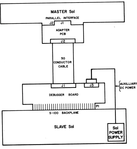
1.1.1 PHYSICAL CONFIGURATION
The ParaSol consists of a main logic board called the Debugger Board and an adapter board which interfaces the Debugger to the Master Sol
(known-good Sol) through its parallel interface connector. The Debugger board plugs into the S-100 bus connector of the Slave Sol
(unit to be debugged). The kit includes necessary cables and a cassette containing the Debugger Program.
1.1.2 OPERATION
The ParaSol Debugger allows the known-good Sol to automatically test
the slave Sol. If the tests do not uncover a problem in the buses or
memory of the slave Sol, the ParaSol then allows you to trace through the personality module program of the slave Sol, single stepping one cycle at a time, or running at high speed until a breakpoint is
reached. You can even examine the contents of the CPU registers of the slave Sol while the program is running.
MASTER Sol
PARALLEL INTERFACE
[image:5.611.80.559.141.664.2]J2 JI
...
-
..
ADAPTER PCB
J2
50 CONDUCTOR
CABLE
J I
DEBUGGER BOARD
S -100 BACKPLANE
SLAVE Sol
PI
Sol
POWER
SEc'rION 2
ASSEMBLY AND HARDWARE CHECKOUT
2.0 INTRODUCTION
1. Unpack the unit and check contents against parts lists in 2.4 of
this section.
2. Visually check the PCBs for defects.
3. using an ohmeter, check to see there are no shorts between the DC
power buses and GND.
2.1 ASSEMBLY OF ParaSol DEBUGGER BOARD
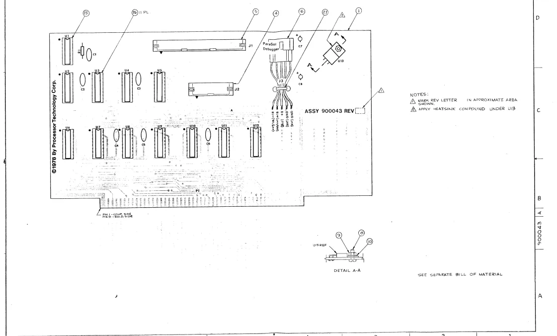
(Refer to Fig. 6-1, ParaSol Debugger PCB Assembly and 2.4, Parts List.)
1. Install Rl.
2. Install 14-pin DIP socket at Ul.
3 • Install 16-pin DIP sockets at U2 through U12.
4. (Optional:) Install test point loop at PI, pin 50, GND.
5. Install capacitors Cl through CS. Observe polarity of C7 and CS.
6. Install header Jl. Pin 1 is indicated by molded triangle on
header. Orient with triangle as shown on assembly drawing.
7. Install 20-pin header J2. Observe same polarity as Jl.
S. Install regulator IC U13. Apply heatsink compound between PCB
surface and bottom of the regulator. (Refer to Detail A-A on Fig.
6-1.
9. Install J3, Sol backplane DC power cable assembly. Proper
orientation is criticall The two white wires should be toward the
regulator. The white/yellow wire should be toward J2. Fasten the
cable assembly with plastic cable tie for strain relief.
10. Using a VOM, check for shorts between +8 VDe and GND (across C7). Check between +5 VDC and GND (across C8).
11. Plug the PCB into the known-good Sol backplane and check +8 VDe across C7. Check for +5 VDC across C8.
12. If OK, unplug PCB from backplane and install ICs Ul through U12. 13. Sight under ICs for bent out or bent under pins.
14. Mark Rev. level on component side of PCB. (Refer to Fig. 6-1, note 1.)
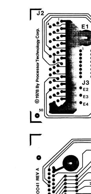
2.2 ASSEMBLY OF CABLE ADAPTER BOARD
(Refer to Fig. 6-2, ParaSol adapter PCB and corresponding parts list in Sec. 7.)
2.2.1 INSTALLATION OF CONNECTORS
1. On the component side of the PCB, install the 25-pin PC-mount socket connector at Jl. Solder all pins and check for shorts and bad solder joints.
2. Mount the header end of the 50-conductor ribbon cable assembly on the component side of the adapter board. Solder and check for shorts and bad connections.
2.2.2 INSTALLATION OF Sol REV LEVEL CONFIGURATION SOCKET
The adapter board is wired to match the parallel I/O connector signals of Sols of rev E and above. Below rev E, the signals PID0 through PID7 are in reverse order. The following procedure allows the adapter board to be configured for any revision of the Sol. (parts for this modification are not provided in the kit.
1. On the trace side of the cable adapter PCB, cut each of the 8 traces between the two vertical rows of socket pads provided for a l6-pin socket at J3. Cut them down the middle.
2. Install a l6-pin socket on the component side at J3.
3. Make a Rev. E configuration plug from a l6-pin component carrier by reconstructing with jumper wire the pattern of the traces which you cut in step 1. Check for shorts and bad solder joints.
4. Wire a second configuration plug for rev 0 and lower from another l6-pin component carrier by reversing the connections to pins 9
Table 2-1. Pin Connections for Configuration Plugs REV E PIN CONNEC'rIONS REV D PIN CONNECTIONS
FROt-l TO FROM TO
1 16 1 9
2 15 2 10
3 14 3 11
4 13 4 12
5 12 5 13
6 11 6 14
7 10 7 15
8 9 8 16
2.3 TEST PROCEDURE
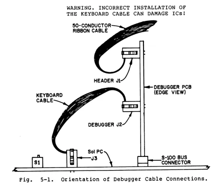
(Refer to Fig 2-1, System Interconnect Diagram.)
1. Connect the female end of the 50-conductor flat cable to the header Jl of the Debugger PCB. Observe the orientation of pin 1. A colored
stripe on one side of the cable and an arrow on the cable connector indicates pin 1. Proper orientation will result in the cable leading off from Jl toward J2. (Refer to Fig. 2-2, Orientation of Debugger Cable Connections.)
~O-CONDUCTO RIBBON CABLE
DEBUGGER J
Sol PC
... - J 3
DEBUGGER PCB (EDGE VIEW)
Fig. 2-2. Orientation of Debugger Cable Connections.
[image:8.611.109.516.372.689.2]CAU'I'ION
Once the flat cable is installed, do not remove
unless necessary. The cable and header are not
built for trequent removal and re-installation.
2. Disconnect the backplane power cable from the backplane of a Sol,
and mate it with the J3 power connector on the debugger board. Do not plug the debugger Boara into the S-100 Bus of the Sol. Place the
debugger Board on a piece of cardboard or other non-conductive material so there is no possibility of shorts.
3. Next plug the 25-pin connector on the cable adapter board into the
parallel I/O connector (J2) of another Sol.
4. Apply power to both Sols.
5. Use the ENTR command to load the following program into the Sol
which has the adapter board installed (referred to as the master Sol) •
C900 C90l C903 C905 C907
AF 03 FA 3E 08 D3 FA
C3 00 C9
XRA A
OUT 0FAH MVI A,8 OUT 0FAH JMP IOC900H
PIE HIGH
PIE LOW
OVER AND OVER
6. Now EXEC C900. The PIE signal on pin 5 of Ul on the debugger
board should be a square wave with a normal TTL swing.
7. Change the byte at C904 to 10 hex; then EXEC C900 again. The PUS
signal on pin 1 of Ul on the debugger board should be a square wave with a normal TTL swing.
8. Enter the following program to check the keyboard register:
C900 3E 0~ MVI A,0
C902 03 FA OUT 0FAH SELECT KEYBOARD REG.
C904 3C INR A
C90s 03 FO OUT 0FOH LOAD KEYBOARD REG.
C907 C3 04 C9 JMP 0C904H LOOP
9. EXEC C900. PIE should be high and PUS should be low. All 8
outputs of the keyboard register should be square waves. KBOI should be oscillating at half the rate of KBD0, KBD2 should be half the rate of KBDl, etc. The outputs of the keyboard register are pins 11, 12, 13, and 14 of U4 and US.
10. Enter the following program to check the DIO register, and the
C900 3E 10 MVI A,10H
C902 D3 FA OUT 0FAH SELECT CONTROL REG.
C904 AF XRA A
C905 D3 FD OUT 0FDH ENABLE DIO REGISTER
C907 3E 18 MVI A,18H
C909 D3 FA OUT 0FAH SELECT DIO REG.
C90B 3C INR A
C90C D3 FD OUT 0FDH LOAD DIO REG.
C90E C3 0B C9 JMP 0C90BH LOOP
11. EXEC C900. PIE should be low, PUS should be high. Pins 1 and 2
of the DIO register ICs, U3 and U7 should be low. All 8 outputs of
the DIO register should be square waves with the same rate
relationship as the keyboard register outputs during the previous test. The DIO register outputs are pins 3, 4, 5, and 6 of U3 and U7.
12. Enter this program to test the control register:
C900 3E 10 MVI A,10H
C902 D3 FA OUT 0FAH SELECT CONTROL REG.
C904 3C INR A
C905 D3 FD OUT 0FDH LOAD CONTROL REG.
C907 C3 04 C9 JMP 0C904H LOOP
13. EXEC C900. The outputs of the control register should all be
square waves as in the previous two tests. These outputs are pins 3,
4, 5, and 6 of U6 and U8. The signal at pin 8 of Ul should be a narrow
pulse which goes low for a period of 1/2 to 1 microsecond.
All debugger board outputs are now tested. Inputs are tested at the
beginning of the debugger program. If a bad input is detected the
system stops with all signals in a static state so the error can be
easily traced.
2.4 PARTS LIST - PARASOL DEBUGGER, TOP ASSEMBLY (900038A)
ITEM #
3
REFERENCE
PART # QTY CODE
727051 1
STANDARD PART#/DESCRIPTION
Cassette, Software, Parasol Debugger
PARTS LIST - PARASOL DEBUGGER, PCB ASSEMBLY (900043A)
1 4 5 6 8 9 10 12 13 14 15 16 18 19 20 21 22 23 25 26 27 28
PART #
900040 717002 717003 103003 720024 720011 720041 707034 707036 707032 707023 707011 701162 701124 701188 701134 701077 701142 713004 713006 722011 721000 REFERENCE
QTY CODE
1
1 J2
1 Jl
1 J3
1
1 1
1 Rl
1 C7
1 C8
5 C2,3,4,5,6
1 Cl
1 U13
1 Ul
1 U2
4 U9,10,11,12
4 U3,6,7,8
2 U4,5
1 Ul
11 U2-U12
1
A/R U13
STANDARD PART #/DESCRIPTION
Fab, PCB, Parasol Debugger Header, Male, PC, 20 Pin Header, Male, PC, 50 Pin
ASsy, Power Cable, Sol Backplane Board
Pan Head Machine Screw, 6-32 x 3/8
Hex Nut, 6-32
Internal Tooth Lock Washer, #6 Resistor, 560 ohms, 1/4 W, 5%
Cap, l5uf, Tant, 20 V, 10%
Cap, 1.0 uf, Tant, 35 V, 10% Cap, .047 uf, Disc Cer, +80-20% Cap, 680 pf, Disc Cer, 10%
7805,* LM340T-5, Volt Reg., +5 74LS132, Quad 2-Input Nand 8T98, Hex Buf/Inv
74LS153, Dual 4-to-l Line MPX
74173, 8T10, TRI-State 4 Bit Latch 74LS163, Synch 4-Bit Bin Cntr
Socket, DIP, 14-pin Socket, DIP, l6-pin Tie, Cable, Plastic Heatsink Compound
PARTS LIST - PARASOL ADAPTER, PCB ASSEMBLY, (900042A)
REFERENCE
ITEM # PART # QTY CODE STANDARD PART #/DESCRIPTION
1 900041 1 Fab, PCB, Parasol Adapter
4 900032 1 J2 Assy, Cable, 50 Cond, Gen. Purpose
5 717011 1 Jl Socket, 25-Pin, PC
6 720013 2 Pan Head Machine Screw,
4-40 x 7/16"
7 720038 2 Internal Tooth Lock Washer, #4
8 720020 2 Hex Nut, 4-40
SECTION 3
HARDWARE THEORY OF OPERATION
3.1 OVERVIEW
The ParaSol Debugger contains the logic necessary to connect the
parallel interface of a master Sol to 5-100 bus of a slave Sol. This is a master slave relationship since the Sol whose parallel interface is connected to the ParaSol is in control of the slave Sol. The master sol can act as a tront panel for the slave Sol, displaying the address bus, data bus, and status signals of the slave Sol. The master Sol can start, stop, or single step the Slave. The master Sol can
automatically test the buses and memory of the slave Sol as well as trace through a program sequence.
A program in the master Sol controls all the operations of the paraSol. The logic on the Debugger board allows input/output
instructions which reference the parallel interface of the master Sol to access the address, data, status, and control signals of the 5-100 bus of the slave. These control signals are XRDY,
ITrGl,
PRESET,MWRITE, FRDY,
DO DSBL,
and PHANTOM. XRDY is used to stop the CPU of the slave Sol mid-way through a machine cycle. While stopped, the master Sol can then input the data on the buses of the slave, or use ITTGT to substitute data from a register on the Debugger board for the data from the slave's memory.An 8080 instruction cycle is defined as the time required to fetch and execute an instruction. Every instruction cycle consists of one to five machine cycles. The ParaSol debugger single steps one machine cycle at a time. A machine cycle is the sequence of events that occur when the 8080 accesses memory or an I/O port. Each machine cycle
consists of three to five T-states of 500 nanoseconds each. The timing of signals during the T-states of a machine cycle cannot be monitored or controlled by the ParaSol Debugger. Refer to the 8080 Microcomputer Systems Users Manual from Intel for detailed information on the
operation of the 8080.
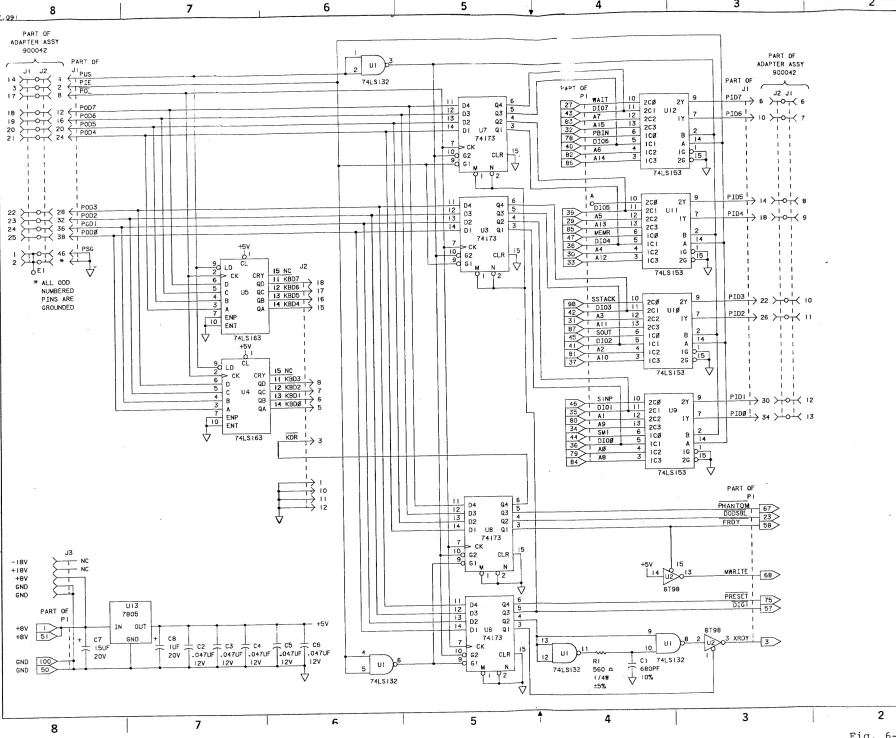
3.2 THE Sol PARALLEL INTERFACE
The ParaSol Debugger interfaces to the master Sol through the parallel interface connector at the rear of the unit. Data is sent to the
Debugger on the eight lines named POD0 to POD7. The signal POL (low active) is the output strobe. Data is received from the Debugger on the eight lines named PID0 to PID7. The 8080 accesses these data lines through port FD (hex). The signals PIE and PUS are Sol output lines used to select the source or destination of data within the
debugger. The 8080 controls PIE through bit 3 of port FA (hex): PUS is controlled by bit 4 of the same port.
3.3 THE PARASol PARALLEL INTERFACE
A 50-conductor flat cable forms a path for the parallel interface signals between the master Sol and the debugger board. An adapter board on the Sol end of the flat cable connects the signals to the even-numbered conductors, and ground to all odd-numbered conductors. The interface signals enter the debugger board through a 50-conductor header designated Jl.
The eight PID lines connect to the outputs of 74LS153 four-to-one multiplexers, U9,U10,Ull, and U12. The POD lines connect to the data
inputs of three 8-bit registers. The keyboard data register is made up of two 74LS163 ICs, U4 and U5. The 010 register, U3 and U7,
consists of two 74173 ICs. The control register is made up of two more 74l73s, U6 and U8. The signals PIE and PUS connect to the select
inputs of the four-to-one multiplexer to control which group of S-100 bus signals will be placed on the PID lines. PIE and PUS also connect to the enable inputs of the ICs that make up the three 8-bit
registers. The clock inputs of the three registers are all connected to the signal
POL.
When POL makes a transition from low to high the data on the POD lines is loaded into the register enabled by PIE and PUS.3.4 THE PARASol S-100 INTERFACE
Inputs to the ParaSol Debugger from the S-100 bus of the slave Sol are multiplexed onto the PIO lines in four groups. One group consists of the eight DIO lines. Address lines A0 to A7 and A8 to A15 form two other groups. The following status signals form the last group:
PID Line PI00 PIOI PI02 PI03 PID4 ~105 PI06 PID7
Status Signal SMI
SINP SOUT SSTACK MEMRITE
*
POBIN PWAIT
*PI05 is not connected to the S-100 bus. Op-tionally, it could be connected to a test probe or auxilliary input.
Bit 3 of the control register controls the 5-100 signal PRESET (low active). When bit 3 is low the 8080 of the slave Sol is reset. When bit 4 of the control register is low the 5-100 signal FRDY (low
active) disables the MWRITE tri-state driver in the slave Sol, and a tri-state driver on the Debugger board forces MWRITE low (inactive). In this state the memory of the sla~e Sol is write-protected. The S-100 signal DO
DSBL
(low active) which disables the tri-state drivers between the 8080 of the slave Sol and the 010 bus is controlled by bit 5 of the control register. Bit 6 of the control register is connected to the 5-100 signal PHANTOM (low active) in the slave Sol. This signal causes the personality module of the Sol to be addressed at location zero. Finally, bit 7 of the control register activates the signal KDR(low active) at the twenty pin header on the Debugger board (J2) used to connect to the keyboard input of the slave Sol. When Bit 7 makes a positive transition, the KDR flip-flop in the slave Sol is set to
indicate that keyboard data is ready.
The 5-100 lines designated 0100 to 0107 are connected to the tri-state outputs of the 010 register. When these outputs are enabled by bit 2 of the control register the contents of the 010 register is placed on the 010 bus of the slave Sol.
The outputs of the keyboard register are connected to the appropriate pins of the 20-pin header on the Debugger board (J2) used to connect to the keyboard input of the slave Sol via a flat cable.
3.5 CONTROL SEQUENCES
The ParaSol Debugger is controlled by input and output instruction sequences of the program in the master Sol. A sequence normally begins with an output to port FA (hex). Bits 4 and 5 of this port control the parallel interface signals PIE and PUS which are used by the debugger to select the source or destination for data. Table 3.1 below
summarizes the PIE and PUS selection codes.
Table 3-1, PIE and PUS SELECTION CODES
PUS PIE SOURCE DESTINATION 0 0 A8 to A15 Keyboard Register
0 1 A0 to A7 Keyboard Register 1 0 010 Bus Control Register
1 1 Status 010 Register
~
~. I.Q
.
w
I
~
.
tU
n,J
Ii
n,J
Ul
0 ~
~
C
::l
0
rt
~.
0
::l n,J
~
trJ ~ 0 0
~ 0
~.
n,J
I.Q
Ii
n,J
E1
tU
n,J
Ii
n,J
Ul
0 ~
KEYBOARD
REGISTER
J3 OF
SLAVE Sol
CONTROL
REGISTER
J2 PARALLEL INTERFACE
CONNECTOR OF MASTER Sol
---_/\~---I
010
REGISTER
010
PID
LINES
4-INPUT MULTIPLEXER
8 BITS WIDE
~ STATUS
LINES BUS
\~---~
V
ADDRESS BUS LINES /S-IOO BUS OF
SECTION 4
SOFTWARE THEORY OF OPERATION
4.J INTRODUCTION
This section includes instructions for loading the source files of the Debugger program, descriptions of the subroutines used in the program, flow charts of test routines, and a source listing of the debugger program.
4.1 TRANSFERRING SOURCE FILES TO DISK
Follow this procedure to load the source files for the Debugger
program and transfer them to PTDOS disk files. Note that these files are not directly compatible with the ALS-8.
1. Insert a PTDOS System diskette in the disk drive. Enter the command: BOOT
2. Connect a tape recorder to the Sol as described in Section 7 of the Sol Systems Manual. This Sol must also have a Belios II Disk System installed.
3. Place the cassette tape in the recorder; depress the play lever, and enter this command: GET PSRCl
4. When the file is loaded, the Sol will display the first address, and the load count like this: PSRCI XXX X YYYY
The first address is represented here by XXXX; the load count is
represented by YYYY. write down these two numbers since they will be erased from the screen shortly.
5. TYPE: EX BCB0.
6. When the PTDOS prompt (*) appears, use the two addresses you wrote down when the cassette file was loaded in this PTDOS command: WRITE PSRCl,XXXX,>YYYY
7. ~epeat this procedure from step 4 for the two remaining files, PSRC2 and PSRC3.
8. To return to SOLOS from PTDOS, use the command EXEC C004. To reenter PTDOS from SOLOS use the command EXEC BCB0.
4.2 4.2.1
BASIC PARASol SUBROUTINES SETCTL
This routine is called to change the contents of the control register on the debugger board. A RAM buffer named CTLSAV is updated by
Example 1: Set PRESET low. LOA CrLSAV ANI FF-RESET CALL SETCTL Example 2: Set PRESET high.
4.2.2
LOA CTLSAV ORI RESET CALL SETCTL SETDIO
GET CURRENT CONTENTS AND WITH F7 hex
CHANGE CONTROL REG.
GET CURRENT CONTENTS OR WITH 08 hex
CHANGE CONTROL REG.
This subroutine is called to load the 010 register. When called, the value in the accumulator is transferred to the 010 register. No
registers or flags are altered.
Example: Load 010 register with C3 hex.
4.2.3
MVI A,0C3H CALL SE'rDIO SETKBD
ACCUMULATOR=C3
010 REGISTER=C3
This routine is called to simulate the depression of a key on the
keyboard of the slave Sol. The value in the accumulator is sent to the slave Sol. The accumulator and flags are altered.
Example: Simulate depression of the A key:
4.2.4 GETDIO
MVI A,'A'
CALL SETKBD ACCUMULATOR=A SEND TO SLAVE
Call this subroutine to move the contents of the 010 bus of the slave Sol to the accumulator, and to the RAM buffer OIOBUF.
4.2.5 GETSTA
Call this subroutine to move the contents of the status lines of the slave Sol to the accumulator and the RAM buffer SBUF.
4.2.6 GETADR
Call this subroutine to move the contents of the address bus of the slave Sol to registers Hand L and to the RAM buffer ADBUF. The
accumulator is altered by this subroutine. 4.2.7 SSTEP
Call this subroutine to allow the slave Sol to complete the current machine cycle and begin the next cycle. The accumulator and flags are altered.
4.2.8 MITST
This subroutine returns with the zero flag set if the current machine cycle is an instruction fetch cycle. The accumulator and flags are altered.
4.2.9 FINOMI
If the current cycle is not a fetch cycle, this subroutine will call SSTEP until a fetch cycle is reached. If the current cycle is an
instruction fetch cycle, FINOMl, will return without single stepping. The accumulator and flags are altered.
4.2.10 TILMI
This subroutine first calls SSTEP then checks for an instruction fetch cycle. If necessary the process is repeated until an instruction fetch cycle is reached. TILMI differs from FINOMI in that if the current cycle is an instruction fetch cycle, TILMI will single step to the next instruction fetch cycle~ FINOMI will not.
4.2.11 AJAM
This subroutine is used to jam the contents of the accumulator into the 8080 of the slave Sol. To accomplish this, the subroutine loads the 010 register, calls SETCTL to activate the
fiTGI
signal, checks that the 010 bus matches the data, and finally calls SSTEP. If the010 bus does not match the data, a jump to the error routine DIBAB takes place. The B-register and flags are altered.
4.2.12 POKE
Call this subroutine to move the contents of the accumulator to the memory locaton pointed to by register-pair HL. This is like a MOV M,A
instruction except that the memory referenced is in the slave Sol. No registers or flags are altered.
4.2.13 PEEK
Call this subroutine to move the contents of the memory location pointed to by register-pair HL to the accumulator. This is like a MOV A,M instruction except that the memory referenced is in the slave Sol. The accumulator is altered.
Example: Move location 1000 in the slave Sol to the accumulator.
4.2.14 PORTI
LXI H,1000H CALL PEEK
POINT HL GET THE OATA
Call this routine to move the data at an input port to the
Example: Load the accumulator from port FF hex of the
slave Sol.
4.2.15 JUMPI
lvlV I A, ~ F F H
CALL PORTI
PORT TO BE READ GET THE DATA
Call this routine to cause the slave Sol to jump to the address in register-pair HL. The accumulator and flags are altered.
Example: Jump slave Sol to address C000 hex:
4.3
4.3.1
LXI H,0C000H CALL JUMPI
I/O ROUTINES
OSOUT
DESIRED ADDRESS JUMP THERE
Call this subroutine with the character to be output in register-B.
4.3.2 INA
This subroutine waits for a character from the keyboard. If the ESCAPE key is pressed this routine exits to SOLOS. If any other key is
pressed it is returned in the accumulator and register-B.
4.3.3 INCHR
This subroutine checks the keyboard once. On return, if a key has been pressed and it is not the ESCAPE key, the character is in the
accumulator and B-register, and the zero flag is reset. If no key has been pressed, the zero flag is set. If the ESCAPE key has been pressed this subroutine returns control to SOLOS.
4.3.4 ADOUT
This subroutine prints the contents of register-pair HL as a 4 digit hex number.
4.3.5 HEXA
This subroutine prints the contents of the accumulator as a 2 digit hex number.
4.3.6 BINOT
This subroutine prints the contents of the accumulator as a binary number.
4.3.7 BINOX
This Subroutine is similar to BINOT except that instead of printing a binary number with ones and zeros, the character in register L is substituted for zeros, and the character in register H is substituted
for ones. This subroutine is used to print the error report for the RAM tests.
4.3.8 AOUTB
Call this routine to print the contents of register pair HL as a binary number.
4.3.9 TEXTO
This subroutine is called to print strings of text. Register-pair HL should be loaded with the address of the beginning of the string. When the up-arrow character (A) is encountered in the string, all the
characters until the next up-arrow character are converted to control characters. The slash character (/) terminates the string.
Example:
LXI H,MSGI CALL TEXTO
prints as:
4.4 FLOW CHARTS
LINE 1 LINE 2 LINE 3
POINT TO STRING PRINT IT
The following flowcharts depict the 'test routines run during the Test Mode 'by the Debugger program. They are presented here to provide
YES
PWAIT SHOULD BE 1 WITH XRDY AT ~.
PRESS: C/R TO RESTART PROGRAM
AFTER RESET ADDRS, BUS SHOULD BE .0.000
INSTEAD OF 'AAAA'. PRESS: C/R ...
SMl SHOULD BE 1 AFTER RESET. PRESS: C/R ...
PDBIN SHOULD BE 1 FOR INST. FETCH. PRESS: C/R ...
PDBIN SHOULD BE
.0 WITH DIGl AT 0.
PRESS: C/R ...
DIO BUS SHOULD BE
00 INSTEAD OF XX, PRESS: C/R ...
TEST CONTROLS
4-6
AFTER 1 CYCLE ADDRS. BUS SHOULD BE .0.0.01 INSTEAD
NO
TEST ADDRESS BUS
rOReE SLAVE - Sol TO JU:-1P TO TLST l'ATTL:R."J
ADDRESS
FORCE SLAVE Sol TO JUMP TO TEST PATTERN
ADDRESS
ADDRESS BU~ SHOULD BE AAAA INSTEAD OF AAAA
NO
TEST oro BUS
WRITL & READ INCREMENTINC; PATTERN TO
010 BUS
010 BUS SHOULD BE 'NN' INSTEAD OF 'NN'.
TEST INTERNAL BUS & PERSONALITY MODULE
NO
COMPARE DATA IN MASTER Sol PERSONALITY MODULE WITH DATA IN SLAVE
Sol
PERSONALITY M:lDULE ERROR AT ADDRESS AAAA INT BUS SHOULD BE NN INSTEAD OF NN
PRESS: C/R ...
4-8
KEYBOARD INTERFACE TEST
KEYBOARD DATA SHOULD BE NN INSTEAD OF NN PRESS: C/R ...
TEST VIDEO RAM
SCREEN RA~ ERROR: 'XXGG GGGX' PRESS: C/R ...
TEST SYSTEM RAM
SYSTEM RAM ERROR: XGGX GGGG PRESS: C/R ...
INCREMENT MEMORY POINTER
INCREMENT MEMORY POINTER
lK MEMORY TEST
ROTATE: WORKING PATTERN LEFT THROUGH CARRY
(RALl
ROTATE WORKING PATTERN LEFT
ROTATE MASTER PATTERN LEFT THROUGH CARRY
(RAL)
NO
4.5 SOURCE LISTING
The Source listing which follows is included in this manual to
encourage and assist you in expanding the usefulness of the Debugger program. It may also be of assistance when_a question arises as to how the program has identified an error.
0~18 0010 0000 0010 0018 00130 '1008 00FA 00FD 00FC 0001 0002 0004 '1008 0010 0020 0040 0080 00FF
~000 C3 0C 00
0003 31 FF CS 0006 CD 73 02 0009 C3 E1 04
000~ **************~***************
a001 ** ParaSol Debugger Program **
0002 ** **
0003 ** Rev. A **
0004 ** **
0005 ** 4/1/78 **
0006 ** **
0007 ** Copyright (C) 1978, by **
0008 ** Processor Technology -*
0009 ** Corporation **
0010 ** All rights reserved. **
0011 ******************************
0012 * 0013 *
0014 0015 0016 *
ORG XEQ
o
o
0017 ** PIE & PUS SELECTION EQUATES 0018 *
0019 ** DATA DESTINATIONS 0020 *
0021 OUTDIO 0022 OUTCTL 0023 OUTKBD 0024 *
BQU EQU EQU
18H . 10H
o
DIO REGISTER CONTROL REGISTER KEYBOARD REGISTER
0025 ** DATA SOURCES 0026 *
0027 INDIO 0028 INSTAT 0029 INHIAD 0030 INLOAD 0031 *
EQU EQU EOU EQU
0032 ** PORT EQUATES 0033 *
0034 SELECT 0035 DATA 0036 KPORT 0037 *
EQU EQU EQU 10H 18H o 8 0FAH 0FDH 0FCH
010 BUS STATUS A8 TO A15 A0 TO A7
PIE PUS PORT DATA PORT KEYBOARD PORT
0038 ** CONTROL REGISTER BIT EQUATES 0039 *
0040 STOP 0041 STEP 0042 JAM 0043 RESET 0044 FRDY 0045 DODSB 0046 PHNTM 0047 KDR 0048 * 0049 FF 0050 * 0051 *
EQU EQU EOU EQU EQU EQU EQU EQU EQU
1 STOP/RUN BIT
2 SINGLE STEP BIT
4 DIG1 CONTROL BIT
8 RESET BIT
10H FRDY BIT
20H DO DSBL BIT
40H PHANTOM BIT
80H KBD. STROBE BIT
0FFH
0052 *****************************************
0053 ** MAIN ROUTINE. EXECUTION BEGINS HERE **
0054 *****************************************
0055 * 0056 * 0057 0058 * 0059 0060 0061 0062 •
JMP LXI CALL JMP MAIN SP,0CBFFH TITLE DISP 4-10
STARTUP FROM 0000 IS NORMAL
STARTUP FROM 0003 SKIPS TESTS
000C 0063 MAIN EQU $
01:10C 31 FF CB 0064 LXI SP,0CBFFH STACK AT TOP OF SOL RAM
0065 *
000F CD 73 02 0066 CALL TITLE ANNOUNCE PROGRAM
0012 CD 3C 00 0067 CALL CKCTL CHECK CONTROLS
0015 CD 26 0B 0068 CALL BOUT SPACE AFTER EACH TEST
0018 CD A0 00 0069 CALL CKDIO CHECK 010 BUS
001B CD 26 0B 0070 CALL BOUT
001E CD C3 00 0071 . CALL CKADR CHECK ADRS BUS
0021 CD 26 0B 0072 CALL BOUT
0024 CD F2 00 0073 CALL CKPER CHECK PERS. MODULE
0027 CD 26 0B 0074 CALL BOUT
002A CD 29 01 0075 CALL CKKBD CHECK KEYBOARD INPUT
002D CD 26 0B 0076 CALL BOUT
0030 CD 3C 01 0077 CALL CKVID CHECK SCREEN MEMORY
0033 CD 26 0B 0078 CALL BOUT
0036 CD 48 01 0079 CALL CKSYS CHECK SYSTEM MEMORY
0039 C3 E1 04 0080 JMP .OISP
0081 *
0082 *
0083 ** THESE ROUTINES PERFORM TESTS. FAILURES ABORT NORMAL 0084 ** RETURN AND RESULT IN JUMP BACK TO MAIN.
0085 *
0086 ** CHECK CONTROL SIGNALS 0087 *
003C 0088 CKCTL EQU $
003C 3E FF 0089 MVI A,FF
003E CD 34 08 0090 CALL SETCTL FREE RUN
0091 *
0041 AF 0092 XRA A
0042 E3 0093 FDLAY XTHL
0043 E3 0094 XTHL
0044 3D 16095 DCR A WASTE TIME
0045 C2 42 00 0096 JNZ FDLAY FOR A WHILE
0097 *
0048 3E F7 0098 MVI A,FF-RESET
004A CD 34 08 0099 CALL SETCTL RESE'r LO
004D E6 FE 0100 ANI FF-STOP
004F CD 34 08 0101 CALL SETCTL NOW XROY LO
0052 F6 08 0102 ORI RESET
16054 CD 34 08 0103 CALL SETCTL THEN RESET HI
0104 *
0057 CO 6A 08 0105 CALL GETSTA GET STATUS
005A E6 80 0106 ANI 80H WAIT HI ?
1:105C CA CD 01 IU07 JZ ERR01 NO --->
16108 *
005F CD 73 08 0109 CALL GETADR GET AORS.
0062 85 0110 ORA L ADRS=0 ?
0063 C2 EO 01 0111 JNZ ERR02 NO --->
0112 *
0066 3A 2F 0C 0113 LOA SBUF GET STATUS
0069 47 0114 MOV B,A
e06A E6 01 0115 ANI 1 M1 HI ?
e06C CA 4C 02 0116 JZ ERR03 NO --->
0117 •
006F 78 0118 MOV A,B
0070 E6 40 0119 ANI 40H POBIN HI ?
0072 CA 55 02 0120 JZ ERR04 NO --->
0121 •
0075 3A 20 0C 0122 LOA CTLSAV GET CTL. BITS
0078 E6 FB 0123 ANI FF-JAM
007A CD 34 08 0124 CALL SETCTL DIG1 LOW
0080 E6 40 0126 ANI 40H POBIN LO ?
~082 C2 5E 02 0127 JNZ ERR05 NO ---)
0128 *
0085 AF 0129 XRA A
0kj86 CO A8 08 0130 CALL AJAM NOP TO TEST Sol
0089 CD 73 08 0131 CALL GETAOR
008C AF 0132 XRA A CHECK AORS
0080 B4 0133 ORA H H=0
008E C2 67 02 0134 JNZ ERR07 NO ---)
0091 70 0135 MOV A,L
0092 3D 0136 OCR A L=l ?
0093 C2 67 02 0137 JNZ ERR07 NO ---)
0096 3A 2D 0C 0138 LOA CTLSAV
0099 F6 04 0139 ORI JAM
009B CD 34 08 0140 CALL SETCTL DIG1 HI
009E AF 0141 XRA A
009F C9 0142 RET CONTROLS OK
0143 *
0144 ** CHECK 010 BUS 0145 *
00A0 3A 20 0C 0146 CKDIO LOA CTLSAV
00A3 E6 DB 0147 ANI FF-JAM-OODSB
00AS CD 34 08 0148 CALL SETCTL OIG1&DO DSBL LOW
00A8 06 00 0149 MVI B,0 INITIALIZE PATTERN
0150 *
00AA 78 0151 CKDll MOV A,B
00AB CD 40 08 0152 CALL SETOIO WRITE PATTERN
00AE CD 61 08 0153 CALL GETDIO READ PATTERN
00B1 B8 0154 CMP B SAME ?
0~B2 C2 A7 01 0155 JNZ DIBAD NO ---)
00B5 04 0156 INR B NEXT PATTERN
00B6 C2 AA 00 0157 JNZ CKDll TILL B=0
0158 *
00B9 3A 20 0C 0159 LOA CTLSAV
00BC F6 24 0160 ORI JAM+DODSB
00BE CD 34 08 0161 CALL SETCTL DIG1&DO DSBL HI
00C1 AF 0162 XRA A
00C2 C9 0163 RET Z SET=DIO BUS OK
0164 *
0165 ** CHECK ADDRESS BUS 0166 *
00C3 21 00 00 0167 CKADR LXI H,0 INITIALIZE PATTERN
00C6 0E 11 0168 MVI C,17 PASS COUNT=17
0169 *
00C8 CD 42 09 0170 CKA1 CALL JUMP1 LOAD TEST PATTERN
00CB CD E2 00 0171 CALL ADCHK CHECK PATTERN
~0CE 29 0172 DAD H
00CF 23 0173 INX H MARCH l ' s
0000 00 0174 OCR C
00D1 C2 C8 00 0175 JNZ CKA1 TILL ALL l ' s
0176 *
1:1004 0E 10 0177 MVI C,16 PASS COUNT
0006 29 0178 CKA2 DAD H MARCH 0's
0007 CD 42 09 0179 CALL JUMP1 LOAD TEST PATTERN
00DA CD E2 00 0180 CALL AOCHK CHECK PATTERN
0000 0D 0181 OCR C
000E C2 06 00 0182 JNZ CKA2 TILL PATTERN=l
1cl0E1 C9 0183 RET ADDRESS BUS OK
01B4 *
00E2 EB 0185 ADCHK XCHG OE=TEST PATTERN
00E3 CD 73 08 0186 CALL GETADR HL=ADRS BUS
00E6 7A 0187 MOV A,D
00E7 BC 0188 CMP H HI BYTE OK ?
00E8 C2 F6 01 0189 JNZ ADBAD NO - - - )
00EB 7B 0190 MOV A,E
00EC BD 0191 CMP L LO BYTE OK ?
00£D C2 F6 01 0192 JNZ ADBAD NO ---)
00F0 EB 0193 XCHG HL=TEST PATTERN
00F1 C9 0194 RET ADRS OK
0195 *
0196 ** CHECK PERSONALITY MODULE
0197 *
00F2 0198 CKPER EQU $
00F2 21 00 C0 0199 LXI H,0C000H P.M. STARTS HERE
0200 *
00F5 CD 0A 09 0201 CKPEI CALL PEEK GET TEST VALUE
00F8 BE 0202 CMP M COMPARE WITH MASTER
00F9 C2 ~4 01 0203 JNZ PMBAD IT'S BAD
0204 *
00FC 23 0205 INX H BUMP POINTER
00FD 7C 0206 MOV A,H
00FE FE C8 0207 CPI 0C8H DONE ?
0100 C2 F5 ~0 02138 JNZ CKPEI NOT YET
0103 C9 02139 RET
0210 *
0104 F5 0211 PMBAD PUSH PSW SAVE DATA
0105 E5 0212 PUSH H SAVE ADDRESS
k'J106 21 C4 03 0213 LXI H,ERM30
0109 CD 613 l1B 0214 CALL TEXTO "AT P.M. ADDRESS "
0215 *
010C El 0216 POP H
010D E5 0217 PUSH H DISPLAY ERROR ADDRESS
0113"£' CD 05 0B 13218 CALL ADOUT
0219 *
0111 21 ED 03 0220 LXI H,ERM31
0114 CD 60 0B 0221 CALL TEXTO "INT BUS S.B."
0117 E1 13222 POP H
13118 7E 0223 MOV A,M
0119 CD 0E 0B 13224 CALL HEXA DISP. CORRECT DATA
0225 *
011C 21 AC 03 0226 LXI H,ERM18
011F CD 60 0B 0227 CALL TEXTO "INSTEAD OF "
0122 F1 0228 POP PSW
0123 CD 0E 0B 0229 CALL HEXA DISPLAY BAD DATA
0126 C3 03 01 0230 JMP ERS
0231 *
0232 ** 'l'EST KBD INTERFACE
0233 *
0129 06 ~0 0234 CKKBD MVI B,0 INITIALIZE PATTERN
0235 *
012B 78 0236 CKBDI MOV A,B
012C CD 46 08 0237 CALL SETKBD PRESS A KEY
012F 3~ FC 0238 MVI A,KPOR'r
~131 CD 53 09 0239 CALL IPORT INPUT KBD PORT
0134 a8 0240 CMP B DATA OK ?
0135 C2 12 02 0241 JNZ KBBAD NO. PROCESS ERROR
0138 04 0242 INR B YES
0139 C2 2B 01 0243 JNZ CKBDI TRY NEXT PATTERN
0244
*
0245 TEST VIDEO RAM
0246
*
013C 21 00 CC 0247 CKVID LXI H,0CC00H SCREEN MEMORY
013F CD 54 01 0248 CALL CKRAM IS TESTED
0142 7B 0249 MOV A,E
0143 B7 0250 ORA A ANY ERRORS ?
0147 C9 0252 RET NO 0253 *
0254 ** TEST SYSTEM RAM 0255 *
0148 21 00 C8 0256 CKSYS LXI H,0C800H SYSTEM SEMORY
014B CD 54 01 0257 CALL CKRAM
014E 7B 0258 MOV A,E
014F B7 0259 ORA A ANY ERRORS ?
0150 C2 42 02 0260 JNZ SYBAD YES
0153 C9 0261 RET NO
0262 *
0263 ** THIS ROUTINE TESTS 1K OF MEMORY BEGINNING AT THE 0264 ** ADDRESS POINTED TO BY HL. ON RETURN E REGISTER 0265 ** BITS WHICH ARE 1 CORRESPOND TO BAD MEMORY BITS. 0266 *
0154 2E 00 0267 CKRAM MVI L,0
0156 7C 0268 MOV A,H
0157 E6 FC 0269 ANI 0FCH FORCE A 1K BOUNDRY
0159 67 0270 MOV H,A
0271 *
015A C6 04 0272 ADI 4
e15C 57 0273 MOV D,A o = H + lK
0274 *
0150 lE 00 0275 MVI E,0 START WITH NO ERRORS
015F 43 0276 MOV B,E MASTER PATTERN = 0
0277 *
0160 48 0278 MPASS MOV C,B C=WORKING PATTERN
0279 *
0161 79 0280 MPOKE MOV A,C A=WORKING PATTERN
0162 CD C8 08 0281 CALL POKE PATTERN TO MEMORY
0282 *
0165 B7 0283 ORA A CARRY=0. PATTERN=0 ?
0166 CA 60 01 0284 JZ SET11 YES. GO INCREMENT
0169 17 0285 RAL ELSE SHIFT IT
~16A C3 6E 01 0286 JMP MTES3 AND UPDATE ADDRESS 13287 *
0160 3C 0288 SET11 INR A INC. PATTERN
0289 *
016E 4F 0290 MTES3 MOV C,A C=NEW PATTERN
016F 23 0291 INX H
0170 7C 0292 MOV A,H
0171 BA 0293 CMP 0 lK FILLED ?
0172 C2 61 01 0294 JNZ MPOKE NO. KEEP POKIN ALONG
0295 *
0175 7C 0296 MOV A,H YES IT~S FULL
0176 DE 04 0297 SBI 4 REWIND ADDRESS
0178 67 0298 MOV H,A
0299 *
0179 48 0300 MOV C,B C=WORKING PATTERN
017A CD 0A 09 0301 MPEEK CALL PEEK CHECK MEMORY
0170 A9 0302 XRA C ANY ERRORS ?
017E CA 83 01 0303 JZ NOERR NOPE
0304 *
0181 B3 0305 ORA E OPPS !
0182 5F 0306 MOV E,A ACCUMULATE ERRORS
0307 *
0183 79 0308 NOERR MOV A,C A=WORKING PATTERN
0184 B7 0309 ORA A CARRY=0. PATTERN=0 ?
0185 CA 8e 01 0310 JZ SET12 YES. INCREMENT IT
0311 *
0188 17 0312 RAL
.
ELSE SHIFT PATTERN0189 C3 80 01 0313 JMP MTES4 AND UPDATE PATTERN
0314 *
018C 3C 0315 SET12 INR A INC. PATTERN 0316 *
0180 4F 0317 MTES4 MOV C,A C=NEW PATTERN
018E 23 0318 INX H
018F 7C 0319 MOV A,H
0190 BA 0320 CMP 0 lK CHECKED ?
0191 C2 7A 01 0321 JNZ MPEEK NOPE
0322
0194 7C 0323 MOV A,H YES
0195 DE 04 0324 SBI 4 REWIND ADDRESS
0197 67 0325 MOV H,A
121326 *
0198 78 0327 MOV A,B
121199 B7 121328 ORA A CARRY=0. MASTER PATTERN=0
019A C2 Al 01 0329 JNZ MTES5 NO. JUST ROTATE
0330 *
121190 04 121331 INR B ELSE UPDATE 'ro 1
019E C3 60 1211 0332 JMP MPASS NEW PASS
0333 *
01Al 17 0334 MTES5 RAL NEW MASTER
01A2 08 0335 RC DONE IF 9 PASSES
01A3 47 0336 MOV B,A ELSE UPDATE PATTERN
01A4 C3 60 01 0337 JMP MPASS NEW PASS
0338 *
0339 ** THESE ROUTINES PROCESS ERRORS, THEN CONTROL GOES 0340 ** BACK '1'0 MAIN THROUGH THE ROUTINE ERS.
0341 *
0342 ** DISP. 010 BUS ERRORS 0343 *
01A7 0344 DIBAD EQU $
01A7 78 0345 MOV A,B
01A8 F5 0346 PUSH PSW SAVE WRITE PATTERN
01A9 21 94 03 0347 LXI H,ERM08
01AC CD 60 0B 0348 CALL TEXTO " 010 S.B."
01AF Fl 0349 POP PSW WRITE PAT.
01B0 CD 2B 0B 0350 CALL BINOT
01B3 21 AC 03 0351 LXI H,ERM18
01B6 CD 60 0B 0352 CALL TEXTO "INSTEAD OF"
01a9 3A 2E 0C 0353 LOA DIOBUF READ PAT.
01ac CD 2B 0B 0354 CALL BINOT
01BF CD 84 0B 0355 CALL CRLF
01C2 3A 20 0C 0356 LOA CTLSAV
I2I1C5 F6 24 0357 ORI JAM+DODSB
01C7 CD 34 08 121358 CALL SETCTL OIGl&DO OSBL HI
01CA C3 03 01 0359 JMP ERS ERROR RETURN
036121 *
I2I1CD 21 7A 02 0361 ERR01 LXI H,ERMl2ll
010121 CD 60 0B 0362 CALL TEXTO "NO WAIT" 0363 *
121364 ** ERRORS END UP HERE 0365 *
0103 21 A4 02 121366 ERS LXI H,ERMll
0106 CD 6121 1218 121367 CALL TEXTO "CR TO RESTART" 0109 CD EF 0A 121368 ERSl CALL INA WAIT FOR A KEY
010C FE 00 0369 CPI eDH CR ?
010E C2 09 01 037121 JNZ ERSI ---> NO
01El 3A 34 168 0371 LOA SETCTL
elE4 F6 04 0372 ORI JAM
01E6 CD 40 08 0373 CALL SETOIO OIGl HI
01E9 B7 B374 ORA A
0lEA C3 0C 00 0375 JMP MAIN START FRESH
0376 •
01F0 CO 60 0B 0378 CALL TEXTO "AoRS. <> 0000"
01F3 11 00 011 0379 LXI 0,0
0380 *
0381 ** oISP. ADRS BUS ERRORS 0382 *
01F6 21 05 02 0383 AoBAo LXI H,ERMI2
01F9 CD 60 0B 0384 CALL TEXTO "ADRS S.B.II
01FC EB 0385 XCHG GOOD AoRS.
01Fo CO 51 0B 0386 CALL AOUTB IN BINARY
0200 21 EF 02 0387 LXI H,ERM22
0203 CD 60 08 0388 CALL TEXTO "INSTEAD OF II
0206 2A 30 0C 0389 LHLD ADBUF BAD ADRS.
0209 CD 51 0B 0390 CALL AOUTB IN BINARY
020C CD 84 0B 0391 CALL CRLF
020F C3 03 01 0392 JMP ERS
0393 *
0394 ** PROCESS KEYBOARD ERRORS **
0395 *
0212 78 0396 KBBAD MOV A,B
0213 F5 0397 PUSH PSW SAVE CORRECT VALUE
0214 21 35 04 0398 LXI H,ERM60
0217 CD 60 0B 0399 CALL TEXTO "KEYBOARD PORT S. B."
021A F1 0400 POP PSW
021B CD 2B 0B 0401 CALL BINOT DISPLAY CORRECT DATA
0402 *
021E 21 EF 02 0403 LXI H,ERM22
0221 CD 60 0B 0404 CALL TEXTO "INSTEAD OF"
0224 3A 2E 0C 0405 LOA DIOBUF
0227 CD 2B 0B 0406 CALL BINOT DISPLAY BAD DATA
022A CD 84 0B 0407 CALL CRLF
0220 C3 03 01 0408 JMP ERS
0409 *
0410 ** PROCESS VIDEO RAM ERRORS **
0411 *
0230 F5 0412 VIBAD PUSH PSW
0231 21 05 04 0413 LXI H,ERM40
0234 CD 60 0B 0414 CALL TEXTO "SCREEN RAM ERROR: "
0415 *
0237 2E 47 0416 MAPX MVI L, ' G '
0239 26 58 0417 MVI H, 'X'
0238 Fl 0418 POP PSW
023C CD 2F 0B 0419 CALL BINOX
023F C3 03 01 0420 JMP ERS
0421 *
0422 ** PROCESS SYSTEM RAM ERRORS **
0423 *
0242 F5 0424 SYBAD PUSH PSW
0243 21 10 04 0425 LXI H,ERM50
0246 CD 60 0B 0426 CALL TEXTO "SYSTEM RAM ERROR: "
0249 C3 37 02 0427 JMP MAPX
0428 *
024C 21 09 03 0429 ERR03 LXI H,ERM03
024F CD 60 0B 0430 CALL TEXTO 115M1 S.B. 1"
0252 C3 03 01 0431 JMP ERS
0432 *
0255 21 2C 03 0433 ERR04 LXI H,ERM04
0258 CD 60 08 0434 CALL TEXTO "PDBIN S.B. 1"
025B C3 03 01 0435 JMP ERS
0436 *
025E 21 55 03 0437 ERR05 LXI H,ERM05
0261 CD 60 0B 0438 CALL TEXTO "PD8IN S.B. 0"
0264 C3 03 01 0439 JMP ERS
0440 •
0267 21 7E 03 0441 ERR07 LXI H,ERM07
026A CD 613 0B 0442 CALL TEXTO "AFTER 5.5."
0260 11 01 013 0443 LXI 0,0001
0270 C3 F6 131 0444 JMP AOBAO DISP. ADRS'S.
0445
0446 ** ANNOUNCE PROGRAM 0447 *
0273 21 4F 04 0448 TI'fLE LXI H,TIMSG
0276 CD 60 0B 0449 CALL TEXTO
0279 C9 0450 RET
0451
0452 ** ERROR MESSAGES 0453 *
027A 5E 4D 4A 5E 0454 ERM01 ASC ""MJ" 'PWAIT' SHOULD BE 1 WITH 'XRDY' AT 0./ 27 50 57 41
49 54 27 20 53 48 4F 55 4C 44 20 42 45 213 31 20 57 49 54 48 20 27 58 52 44 59 27 2~
41 54 20 30 2E 2F
02A4 5E 4D 4A 5E 0455 ERM11 ASC ""MJ"TYPE 'CR' TO RESTART PROGRAM/" 54 59 50 45
20 27 43 52 27 20 54 4F 213 52 45 53 54 41 52 54 20 50 52 4F 47 52 41 40 2F
0456 *
02C5 5E 4D 4A 5E 0457 ERM02 ASC ""MJ"AFTER RESET/ 41 46 54 45
52 20 52 45 53 45 54 2F
02D5 5E 4D 4A 5E 0458 ERM12 ASC ""MJ"ADRS. BUS SHOULD BE: / 41 44 52 53
2E 20 42 55 53 20 53 48 4F 55 4C 44 20 42 45 3A 20 2F
02EF 5E 4D 4A 5E 0459 ERM22 ASC ""MJ'" INSTEAD OF: / 20 20 20 20
20 20 20 20 20 49 4E 53 54 45 41 44 20 4F 46 3A 20 2F
0460 *
0309 5E 40 4A 5E 0461 ERM03 ASC ""MJ"'SM1' SHOULD BE 1 AFTER RESET./ 27 53 4D 31
27 20 53 48 4F 55 4C 44 20 42 45 20 31 20 41 46 54 45 52 20 52 45 53 45 54 2E 2F
032C 5E 40 4A 5E 0463 ERl>104 ASC "AMJft'PDBIN' SHOULD BE 1 FOR INST. FETCH.I 27 50 44 42
49 4E 27 20 53 48 4F 55 4C 44 20 42 45 20 31 20 46 4F 52 20 49 4E 53 54 2E 20 46 45 54 43 48 2E 2F
0464 *
0355 5E 40 4A 5E 0465 ERM05 ASC "-MJ-PDBIN' SHOULD BE 0 WITH 'DIG1' AT 0.1 50 44 42 49
4E 27 20 53 48 4F 55 4C 44 20 42 45 20 30 20 57 49 54 48 20 27 44 49 47 31 27 20 41 54 20 30 2E 2F
0466 *
037E 5E 40 4A 5E 0467 ERM07 ASC "-MJ-AFTER SINGLE STEPI 41 46 54 45
52 20 53 49 4E 47 4C 45 20 53 54 45 50 2F
0468 *
0394 5E 40 4A 5E 0469 ERM08 ASC "-MJ-DIO BUS SHOULD BE: I 44 49 4F 20
42 55 53 20 53 48 4F 55 4C 44 20 42 45 3A 20 2F
03AC 5E 40 4A 5E 0470 ERM18 ASC u-MJ- INSTEAD OF: I 20 20 20 20
20 20 20 49 4E 53 54 45 41 44 20 4F 46 3A 20 2F
0471 *
03C4 5E 40 4A 5E 0472 ERM30 ASC "-MJ-PERSONALITY MODULE ERROR AT ADDRESS I" 50 45 52 53
4F 4E 41 4C 49 54 59 20 4D 4F 44 55 4C 45 20 45 52 52 4F 52 20 41 54 20 41 44 44 52 45 53 53 20 2F
03ED 5E 40 4A 5E 0473 ERM31 ASC "-MJAINT BUS SHOULD BE: I" 49 4E 54 20
42 55 53 20 53 48 4F 55 4C 44 20 42 45 3A 20 2F
53 43 52 45 45 4E 20 52 41 40 20 45 52 52 4F 52 3A 20 20 2F
0476 *
0410 5E 40 4A 5E 0477 ERM50 ASC n-MJ-SYSTEM RAM ERROR: /"
53 59 53 54 45 40 20 52 41 40 20 45 52 52 4F 52 3A 20 20 2F
0478 *
0435 5E 40 4A 5E 0479 ERM60 ASC II-MJ-KBD. PORT SHOULD BE: /n
4B 42 44 2E 20 50 4F 52 54 20 53 48 4F 55 '4C 44 20 42 45 3A 20 2F
8480 *
044F 5E 4B 4A 4A 0481 TIMSG ASC n-KJJJ" Processor Technology Corp."MJJ" n 4A 5E 20 20
20 20 20 20 20 20 20 20 50 72 6F 63 65 73 73 6F 72 20 54 65 63 68 6E 6F 6C 6F 67 79 20 43 6F 72 70 2E 5E 40 4A 4A 5E
047E 20 20 20 20 0482 ASC paraSol Debugger program-MJJ- n
20 20 20 20 20 20 50 61 72 61 53 6F 6C 20 20 44 65 62 75 67 67 65 72 20 20 50 72 6F 67 72 61 60 5E 40 4A 4A 5E
04A7 20 20 20 20 8483 ASC n Rev. A"MJJJ"TESTS IN PROGRESS ... MJJ .. /
20 20 20 20 20 20 20 20 20 20 20 20 20 20 20 20 52 65 76 2E 20 41 5E 40 4A 4A 4A 5E 54 45 53 54 53 20 49 4E 20 50 52 4F 47 52 45 53 53 2E 2E 2E 5E 40 4A 4A 5E 2F
0484 * 0485 *
0488 *******************************
0489 *
0490 *
04E1 0491 DISP EQU $
0492 *
04E1 3E FE 0493 DISPC MVI A,FF-STOP
04E3 CD 34 08 0494 CALL SETCTL SET XRDY LO
04E6 21 B6 09 0495 LXI H,STMSG DISPLAY
04E9 CD 60 0B 0496 CALL TEXTO START-UP MESSAGE
04EC CD 43 07 0497 DISP1 CALL START START-UP P.M.
04EF CD 44 06 0498 CALL BRINI INITIALIZE BREAK CONDITION 0499 *
04F2 3A 37 0C 0500 DISPI LDA SFLAG
04F5 F6 01 0501 ORI 1
04F7 32 37 0C 0502 STA SFLAG FORCE SINGLE STEP MODE
0503 *
04FA CD 84 0B 0504 DISP2 CALL CRLF
04FD CD .6A 08 0505 CALL GETSTA GET STATUS BITS
0500 CO 99 08 0506 CALL M1CHK M1 CYCLE ?
0503 C2 09 05 0507 JNZ NOTM1 NO---)
0506 CD 84 0B 0508 CALL CRLF FOR LF BETWEEN INST'S
0509 CD 2D 07 0509 NOTM1 CALL DISPA DISPLAY CYCLE ON SCREEN 0510 *
050C 0511 DISP3 EQU $
050C CD FF 0A 0512 CALL INCHR GOT A KEY ?
050F C2 1D 05 0513 JNZ DISP4 YES. GO PROCESS
0514 *
0512 3A 37 0C 0515 LDA SFLAG NO KEY. BUT •••
0515 E6 01 0516 ANI 1 ARE WE SINGLE STEPPING ?
0517 C2 0C 05 0517 JNZ DISP3 YES. KEEP CHEECKING KBD.
051A C3 72 05 0518 JMP CYCLE NO. DO ANOTHER CYCLE
0519 *
0520 ** IS IT A COMMAND KEY ? 0521 *
0510 FE 53 0522 DISP4 CPI ' S ' RESTART ?
051F CA E1 04 0523 JZ OISP YES ---)
0522 FE 20 0524 CPI ' , NEXT CYCLE ?
0524 CA 65 05 0525 JZ SINGL YES ---)
0527 FE 4A 0526 CPI ' J ' JUMP 7
0529 CA 5C 06 0527 JZ GOTO YES ---)
052C FE 42 0528 CPI 'B '. BREAK ?
052E CA 78 05 0529 JZ BREAK YES ---)
0531 FE 43 0530 CPI ' C ' RE-BREAK ?
0533 CA CE 05 0531 JZ TRAO YES ---)
0536 FE 46 0532 CPI ' F' FREE RUN ?
0538 CA 7E 06 0533 JZ FREE YES ---)
0538 FE 52 0534 CPI 'R' REGISTER DUMP ?
053D CA A1 06 0535 JZ REGS YES ---)
0536 *
0537 ** MAYBE IT'S A SPEED CONTROL KEY 0538 *
0540 FE 3A 0539 CPI '9' +1 BIGGER THAN 9 ?
0542 D2 72 05 0540 JNC CYCLE YES. DO ANOTHER CYCLE
0545 FE 31 0541 CPI ' 1 ' GREATER THAN 0 ?
0547 DA 72 05 0542 JC CYCLE NO. DO ANOTHER CYCLE
0543 *
0544 * IT IS A SPEED CONTROL KEY 0545 *
0546 * 1-FASTEST, 9- SLOWEST 0547 *
C80B 0548 SPEED EQU 0C80BH SOLOS DISPLAY SPEED PARAMETER 0549 *
054A 06 30 0550 SUI 30H REMOVE ASCII BIAS
054C 4F 0551 MOV C,A
0540 AF 0552 XRA A
054E 37 0553 STC START WITH 1/2
054F 00 0554 SLOWER OCR C COUNT VALUE DOWN
0550 CA 57 05 0555 JZ SETSP
0553 17 0556 RAL MULTIPLY BY 2
0554 C3 4F 05 0557 JMP SLOWER AND LOOP
0558 *
0557 32 0B C8 0559 SETSP STA SPEED LOAD TRANSLATED VALUE
055A 3A 37 0C 0560 LOA SFLAG
0550 E6 FE 0561 ANI 0FEH STOP SINGLE STEPPING
055F 32 37 0C 0562 STA SFLAG
0562 C3 72 05 0563 JMP CYCLE AND DO NEXT CYCLE
0564 *
0565 ** SP KEY=SINGLE STEP 0566 *
0565 3A 37 0C 0567 SINGL LOA SFLAG
0568 F6 01 0568 ORI 1 SET SINGLE STEP FLAG
056A 32 37 0C 0569 STA SFLAG
056D 3E 04 0570 MVI A,4
056F 32 0B C8 0571 STA SPEED SET DISP. SPEED
0572 *
0572 CD 88 08 0573 CYCLE CALL SSTEP STEP ONCE
0575 C3 FA 04 0574 JMP DISP2 AND LOOP
0575 *
0576 ***************************
0577 ** TRACE MODE ROUTINES **
0578 ***************************
0579 *
0580 ** BREAK POINT OPERATION 0581 *
0578 21 E5 09 0582 BREAK LXI H,BRKMS
~57B CD 60 0B 0583 CALL TEXTO ASK FOR SPECIFICATION
057E CD DE 08 0584 CALL GCLIN GET IT
0581 CD 0C 0C 0585 CALL GSAD FIND ON SCREEN
0586 *
0584 CD C2 0B 0587 CALL SKIP FIND CYCLE NAME
0587 CA BD 05 0588 JZ BROP0 THERE ISN'T ONE
058A E5 0589 PUSH H SAVE ITS ADDRESS
058B CD 24 06 0590 CALL SMOVE PUT IN BUFFER
0591 *
058E E1 0592 POP H
058F CD C2 08 0593 CALL SKIP FINO ADDRESS
0592 CA BD 05 0594 JZ BROP0 THERE ISN'T ONE
0595 EB 0595 TRAP2 XCHG DE-SCREEN ADRS.
0596 CD 8F 0B 0596 CALL SHEX1 ASCII TO HEX
0599 CA AS 05 0597 JZ TRAOK VALUE OK --->
059C 21 07 0A 0598 LXI H,QUMES MARK BAD VALUE
059F CD 60 0B 0599 CALL TEXTO
05A2 C3 78 05 0600 JMP BREAK TRY AGAIN
0601 *
05A5 22 35 0C 0602 TRAOK SHLD TADRS SAVE ADDRESS! 0603 *
05A8 3A 38 0C 0604 LOA CBUFF GET CYCLE NAME
05AB 21 3A 06 0605 LXI H,CYTAB NAME TABLE
05AE 11 3F 06 0606 LXI D,OPTAB MASK TABLE
05B1 06 05 0607 MVI B,5
0608 *
0609 * THIS TRANSLATES CYCLE NAME TO STATUS MASK 0610 *
0583 BE 0611 BROP1 CMP M TEST CYCLE NAME
05B4 CA C6 05 0612 JZ BROP2 IT MATCHES 1
05B8 13 0614 INX 0 NEXT STATUS MASK
05B9 05 0615 OCR B
05SA C2 63 05 0616 JNZ SROPI 5 TIMES
05BO 0617 SROP0 EQU $
05S0 21 07 0A 0618 LXI H,QUMES
05C0 CD 60 0B 0619 CALL TEXTO "???"
05C3 C3 78 05 0620 JMP BREAK
0621 *
05C6 78 0622 BROP2 MOV A,B
05C7 32 49 0C 0623 STA CYNUM SAVE FOR LATER
05CA 1A 0624 LOAX 0
05CB 32 48 0C 0625 STA BRKST
0626 *
05CE 21 0C 0A 0627 TRAO LXI H,BRKM2
0501 CD 60 0B 0628 CALL TEXTO "BREAK CONOITION="
0504 21 38 0C 0629 LXI H,CBUFF
0507 CD 60 0B 0630 CALL TEXTO "CY. NAME"
0631 *
050A 2A 35 0C 0632 LHLO TAORS GET TRAP AORS.
0500 3A 49 0C 0633 LDA CYNUM IT'S LATER
05E0 FE 03 0634 CPI 3 IS AN I/O BREAK ?
05E2 OA EB 05 0635 JC TRA01 YES
0636 *
05E5 CD 05 0B 0637 CALL ADOUT ELSE OISPLAN AN
05E8 C3 F3 05 0638 JMP TRA02 ADDRESS
0639 *
05EB 70 0640 TRAOI MOV A,L GET PORT
*
05EC 67 0641 MOV H,A COpy IN H
05EO 22 35 0C 0642 SHLD TAORS RESTORE TO MEMORY
05F0 CD 0E 0S 0643 CALL HEXA DISPLAY IT
0644 *
05F3 21 3A 0A 0645 TRA02 LXI H,BRKM3
05F6 CD 60 0B 0646 CALL TEXTO MENr1'ION ABORT
05F9 CO 88 08 0647 CALL SSTEP FOR C. OPTION
0648 *
05FC CO 71 07 0649 TRAP3 CALL TSTEP BREAK ELSE STEP
05FF CA 1B 06 0650 JZ FOUND SPRING THE TRAP
0602 CO FF 0A 0651 CALL INCHR CHECK KBO
0605 CA FC 05 0652 JZ TRAP3 KEEP STEPPING
0608 FE 53 0653 CPI 'S'
060A CA El 04 0654 JZ OISP RESET IF "s"
0600 FE 41 0655 CPI ' A' ABORT ?
060F C2 FC 05 0656 JNZ TRAP3 NO --->
0612 21 53 0A 0657 LXI H,ABTMS <--- YES
0615 CO 60 0B 0658 CALL TEXTO SAY SO
0618 C3 F2 04 0659 JMP OISPI BACK TO NORMAL
0660 *
061S 21 72 0A 0661 FOUND LXI H,FMSGI
061E CO 60 0B 0662 CALL TEXTO SAY "FOUND"
0621 C3 F2 04 0663 JMP DISPI SHOW IT
0664 *
0624 11 38 0C 0665 SMOVE LXI O,CBUFF COMMAND BUFFER
0666 *
0627 7E 0667 SMOV1 MOV A,M FROM SCREEN
0628 E6 7F 0668 ANI 7FH KILL CURSOR
062A 12 0669 STAX 0 TO BUFFER
062B FE 20 0670 CPI 20H FOUND SPACE ?
062D CA 35 06 0671 JZ SMOV2 YES
0672 *
0630 23 0673 INX H ELSE CONTINUE
0631 13 0674 INX D
0632 C3 27 06 0675 JMP SMOVI
0676 *
0635 13 0677 SMOV2 INX D
0636 3E 2F 0678 MVI A,2FH ' / '
0638 12 0679 STAX D FOR TEX'rO
0639 C9 0680 RET
10681 *
063A 0682 CYTAB EQU $ CYCLE NAME TABLE
063A 46 52 57 49 0683 DB 'F' , 'R' , 'W' , 'I ' , '0' 4F
0684 *
063F 0685 OPTAB EQU $ BREAK STATUS MASKS
063F 11 0686 DB IlH FETCH
0640 10 0687 DB 10H READ
~641 00 0688 DB 00H WRITE
0642 02 0689 DB 02H INPUT
0643 ~4 0690 DB 04H OUTPUT
0691 *
0692 ** INITIALIZATION OF BREAK CONDITION 0693 *
0644 21 56 06 0694 BRINI LXI H, ICY
0647 CD 24 06 0695 CALL SMOVE IS'S A FETCH
064A 3E 11 0696 MVI A,11H
064C 32 48 0C 0697 STA BRKST LOAD STATUS MASK
064F 21 00 00 0698 LXI H,0 ADRS=0000
0652 22 35 0C 0699 SHLD TADRS
0655 C9 0700 RET
0701 *
0656 46 45 54 43 0702 ICY ASC "FETCH " 48 20
0703 * 0704 *
07~5 ** JUMP OPERATION 0706 *
0707 *
065C 21 98 0A 0708 GOTO LXI H,GOTMS
065F CD 60 0B 0709 CALL TEXTO ASK FOR ADRS.
0662 CD DE eB 0710 CALL GCLIN TYPE IN ADRS
0665 CD 0C 0C 0711 CALL GSAD FIND ON SCREEN
0668 EB 0712 XCHG
.
DE=SCREEN ADRS.0669 CD 8F 0B 0713 CALL SHEXl ASCII-)BINARY
066C CA 78 06 0714 JZ GOTOI VALUE OK
0715 *
066F 21 D7 0A 0716 LXI H,QUMES
0672 CD 60 0B 0717 CALL TEXTO MARK ERROR
0675 C3 5C 06 0718 JMP GOTO BAD VALUE
0719 *
0678 CD 42 09 0720 GOT01 CALL JUMPl GO TO IT
067B C3 FA 04 0721 JMP DISP2 AND DISPLAY
0722 * 0723 *
0724 ** FREE RUN OPERATION 0725 *
0726 *
067E 3E FF 0727 FREE MV1 A,FF ALL BITS HI
0680 CD 34 08 0728 CALL SETCTL AWAY WE GO
0683 21 66 09 0729 LXI H,FREMS
0686 CD 60 0B 0730 CALL TEXTO SAY "FREE RUNNING"
0731 *
0689 CD EF 0A 0732 FREEl CALL INA WAIT FOR A KEY
068C FE 53 0733 CPI 's' RESET ?
068E CA El 04 0734 JZ DISP YES ---)
0691 FE 210 0735 CPI STOP AGAIN ?
0693 C2 89 06 0736 JNZ FREEl NO ---)
0696 3E FE 0738 MVI A,FF-STOP <--- YES
0698 CD 34 08 0739 CALL SETCTL READY LO
069B