Multiport Memory Design in Quantum Dot Cellular
Automata Platform
Suparba Tapna
Department of Electronics and Communication Engineering Durgapur Institute of Advanced
Technology and Management Durgapur, India
Kisalaya Chakrabarti
Department of Electronics and Communication Engineering Haldia Institute of Technology
Haldia, India
Debarka Mukhopadhyay
Department of Computer Science and Engineering
Adamas University Kolkata, India
ABSTRACT
Quantum dot Cellular Automata (QCA) is one of the developing patterns in the field of nanotechnology, which is supposed to overcome the constraints of CMOS innovation while integrated to nano-level. QCA can be utilized to structure memory circuits. Static Random Access Memory (SRAM) is one of the appealing utilization of QCA Innovation. The proposed plan and simulation of memory cell dependent on QCA with minimum area and complexity. This paper presents the design and simulation of multiport SRAM in QCA with least number of majority gates and it will be simulated using QCA Designer. SRAM based on QCA has been contrasted with CMOS innovation utilizing Xilinx. The comparison results show that the QCA memory circuit provides high efficiency in terms of area, complexity and power consumption. QCA can be used to design memory circuits. Static Random Access Memory (SRAM) is one of the attractive application with QCA Technology. The proposed design and simulation of memory cell based on QCA with minimum area and complexity. This paper presents the design and simulation of multiport SRAM in QCA with minimum number of majority gates. SRAM based QCA performance has been compared with CMOS technology using Xilinx.
Keywords
QCA, Majority voter gate, Multiport memory, SRAM, CMOS Technology.
1.
INTRODUCTION
Feature size in CMOS has decreased after a drawn-out period of time; regardless, a couple of requirements still exist. This has caused the snappy enhancement of molecular plans on the nanoscale. QCA is one of the nanotechnology has been as of late perceived and it is relied upon to accomplish low zone and power utilization and high exchanging pace. QCA has small voltage source and the situation of electrons decides the consistent qualities [2]. Static random access memory (SRAM) speaks to an appealing use of the QCA innovation. Its structure is entirely reasonable for creation at the nanoscale [3]. The article [4] implemented memory as parallel read/sequential compose. The fundamental target of this paper is a handy reduced multiport Memory cell in QCA. The region and postponement of the QCA-based SRAM cell displayed in this paper was contrasted and the SRAM cell dependent on CMOS and our proposed structure of multiport memory utilized in the plan of SRAM cell has proficiency as far as region and multifaceted nature when contrasted with [1]. The outcomes demonstrates that the proposed SRAM cell performs with a base expended zone. The rest of this paper is sorted out as follows.
2.
QUANTUM DOT CELLULAR
AUTOMATA IN BRIEF
2.1 Review of QCA Cell
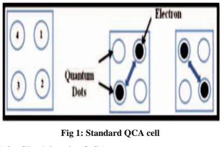
[image:1.595.319.540.424.570.2]Conventional QCA cell is a square shape with four Quantum spots situated at its corners. There are two electrons in every cell that can burrow between two quantum dots in a cell, however they can't burrow between two cells. Initial one demonstrates a standard QCA cell with four specks at the corner. The polarization speaks to rationale expresses that twofold rationale 0 and paired rationale 1. On the off chance that the two electrons adjust in the lower left and upper right dots, it speaks to rationale 1 state speaks to second figure. On the off chance that the two electrons adjust in the upper left and lower right specks, it speaks to rationale 0 state in third figure. Figure 1. (a) QCA cell portrayal (b) Cell polarization = +1 (state 1) (c) Cell Polarization = - 1 (state 0).
Fig 1: Standard QCA cell
2.2 Clocking in QCA
13
Fig 2: QCA clocking phase
2.3 Inverter
A standard structure of the QCA inverter in which the information is given at one of the closures and the altered yield is acquired at the opposite end. The input wire parts into two parallel wires, and due to Columbia fascination it enraptures the cell put toward the finish of these wires on the right hand side to the contrary polarization.
2.4 Majority gate
A fundamental component of QCA circuit is Majority gate; as majority logic can be utilized for executing any logical function as opposed to utilizing Boolean logical operators. A two input AND function can be actualized by a three input majority gate by settling one of its contributions as a logical zero, though on the off chance that one input of a majority gate set to legitimate one it acts like a two input OR function. The essential QCA logic component is a majority gate as shown in Fig. 3.It produces a yield of one if most of the inputs are one.
2.5 QCA Memory cell
In this section, an outline of QCA memory structures is presented. These structures depend on the memory-in movement worldview by which the estimation of the put away information is moved through various cells in a closed loop spanning at least four clocking zones. These structures have diverse highlights, for example, number of bits stored in a loop, get to type (sequential or parallel) and cell plan for the memory bank. The parallel design is like a customary CMOS based memory engineering. The fundamental classical memory cell of this engineering is appeared in Fig. 3. The information bit is put away in a circle, until the WR/RD control flag is low. Whenever WR/RD is raised high, at that point the information bit is put away on the up. The circle must be actualized utilizing all zones of the four stage adiabatic switching technique for the clock, thus allowing the motion of the stored bit. Beginning from the basic cell, a variety of memory cells can be actualized utilizing similar structures utilized in the plan of CMOS memory banks. In a QCA pipelined framework, this enables the put away an incentive to be protected on the up and up until the compose mode happens. The privilege AND gate is called an enable gate and works freely from rest of the circuit. Despite whether one is in the read or write mode, the enable gate yields the stored value when EN is '1'. This demonstrates the memory cell is chosen to be perused. Something else,when EN is '0', the yield is '0', which implies that the memory cell isn't chose to be perused. The circuit schematic for proposed QCA memory cell is appeared in Fig. 3.In the above figure, discloses SRAM keeps on being a fundamental and important memory innovation. It demonstrates the technology of memory cell. In the memory cell when EN = 1, output is
[image:2.595.320.544.128.285.2]enabled and when EN = 0, output = 0. Whenever R/W = 1, the read state is enabled and the D value is saved in the memory circle. Whenever R/W = 0, the read state is enabled and the saved bit is placed on the output.
Fig 3: Basic memory cell
3.
IMPLEMENTATION OF
MULTIPORT MEMORY IN QCA
We have to implement dual port and quad port memory include types of multiport SRAM in quantum dot cellular automata platform.3.1
Dual port memory
This section presents the proposed structure of dual port SRAM and depicts their block diagram. The design of multi-port SRAM requires more than one
Fig 4: Block diagram of dual port memory cell
Port. Here in these case mainly shows the gate-level design of dual port memory. Our proposed structure of dual multi-port which is necessary for designing the one data I/P port and two data O/P port memory. It requires seven i/p ports and it is efficient in terms number of cells and area when compared to secondary memory. To the best of our knowledge dual port architecture is reported for the first time in literature.
[image:2.595.327.539.380.495.2] [image:2.595.317.543.594.751.2]3.2
Memory of Quad port
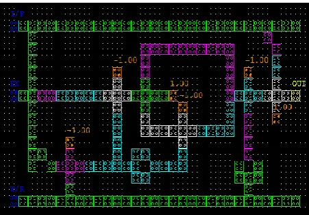
[image:3.595.316.543.72.221.2]The quad port memory cell is designed to obtain the structural difference in QCA. Mainly, there are three cases need to identify to design a multiport memory using tri-state logic gate. First is write operation, second is read operation and last operation is w/r inconsistence. The theoretically semaphore concept is realized to resolve the problem. But practically it is finding out to overcome the problem in current technology research. It is very difficult to say about the priority between three cases is more important than others.
Fig 6: Design of quad port memory cell in Xilinx
4.
MULTIPORT GATE LEVEL
ARCHITECTURE IN CMOS
TECHNOLOGY
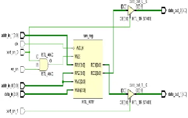
4.1 Design of dual port memory
The study of comparisons between QCA designer and Xilinx (which is based on the CMOS technology) in terms of power consumption, area and complexity. The more efficient technology used in Xilinx, that can be helped to find out the solution to overcome the r/w inconsistence and priority resolver. This paper have two main objectives: i) reduced consumed area ii) achieving minimum complexity.
Fig 7: Design of dual port memory
4.2 Quad port memory execution
In Xilinx tool quad port memory design is basically dependent on the gate level architecture. The approach towards the architecture which is inconsistent with data flow and power dissipation of the entire CMOS technology.
Fig 8: Design of quad port memory
5.
SIMULATION AND RESULTS
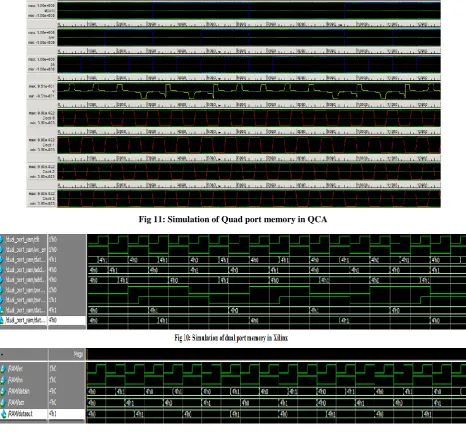
[image:3.595.60.272.187.414.2]The design and simulation of a dual port as well as Quad port SRAM in the QCA technology are presented in this paper. The proposed tri-state multiport memory is a flexible and powerful structure using Programmable logic and interconnections. The design is significantly improved because this memory has a 32-bit width. In comparison with other studies, the presented memory cell acts as a pipeline that decreases delays and increases operating speed. The designs can be implemented using the QCA Designer and simulated by the QCA Designer software tool and also simulated using the Xilinx RTL encounter tool. The results showed that the proposed QCA based dual port performs a task with reduced area and complexity in terms of number of cells when compared to CMOS based memory.
Fig 9: Simulation of dual port memory in QCA
Table 1. Summary of the data obtained from the simulation of the Dual port and Quad port memory in
QCA as well as CMOS Technology
Sl no
.
Circuit compo
nents
QCA Technology using QCA designer
tool
CMOS technology using Xilinx RTL encounter tool
Area Co mpl exit y
Powe r cons umpt ion(F W)
Area Co mpl exit y
Pow er cons ump tion( W)
1 Dual port
0.06 µm2
53 330.8 32m2 109 1.23
2 Quad port
0.22 µm2
[image:3.595.70.265.544.666.2]15
[image:4.595.64.531.78.513.2]Fig 11: Simulation of Quad port memory in QCA
Fig 12: Simulation of Quad port memory in Xilinx
6.
CONCLUSION
The results showed that the proposed QCA based SRAM performs a task with reduced area and complexity in terms of number of cells when compared to CMOS based SRAM.Table 1 shows the comparison between QCA and Xilinx tool. It is a significant improved in terms of area about 0.22 µm2 for quad port and 0.06 µm2 for dual port. Table 1 shows that our proposed structure of multiport SRAM has efficient in terms of area and complexity. Thus our proposed paper have overcome the problems in CMOS technology on nanoscale. It is expected that the reduction method presented in this work would produce significant hardware savings for many future QCA based implementation.
7.
ACKNOWLEDGMENTS
The authors would like to express their thanks to the department of Computer Science and Engineering, Adams University, Kolkata and the department of Electronics and Communication Engineering, Durgapur Institute of Advanced Technology and Management, Durgapur, and Haldia Institute of Technology for the constant infrastructure support. The authors also greatly acknowledge the support of others faculty member of Department of CSE and ECE.
8.
REFERENCES
[1] International Technology Roadmap for Semiconductor (ITRS),Online Available: 〈http://www.itrs.net〉.
[2] V. Vankamamidi, M. Ottavi, and F. Lombardi, “A serial memory by quantum-dot cellular automata (QCA),” IEEE Trans. Comput., vol. 57,no. 5, pp. 606–618, May 2008.
[3] I. Amlani, A. O. Orlov, G. Toth, G. H. Bernstein, C. S. Lent, and G. L. Snider, “Digital logic gate using quantum-dot cellular automata,” Science, vol. 284, no. 5412, pp. 289–291, 1999.
[4] C. R. Graunke, D. I. Wheeler, D. Tougaw, and J. D.Will, “Implementation of a crossbar network using quantum-dot cellular automata,” IEEE Trans. Nanotechnology, vol. 4, no. 4, pp. 435–440, July. 2005.
[5] M. Ottavi, S. Pontarelli, V. Vankamamidi, A. Salsano, and F. Lombardi,“QCA memory with parallel read/serial write: Design and analysis,” IEE Proc. Circuits, Devices Syst., vol. 153, no. 3, pp. 199–206, Jun. 2006.
and memory structures,” Microelectron. J., vol. 43, no. 12, pp. 929–940, 2012.
[7] R. Sabbaghi-Nadooshan and M. Kianpour, “A novel QCA implementation of MUX-based universal shift register,” J. Comput.Electron., vol. 13, no. 1, pp. 198– 210, 2014.
[8] Cho and E. E. Swartzlander, “Adder and multiplier design in quantumdot cellular automata,” IEEE Trans. Comput., vol. 58, no. 6, pp. 721–727, Jun. 2009.
[9] Douglas Tougaw and Mahfuza Khatun.” A Scalable Signal Distribution Network for Quantum-Dot Cellular Automata” IEEE Transactions on Nanotechnology, vol. 12, no. 2, March 2013.
[10] .Perri, P. Corsonello, and G. Cocorullo, “Area-delay efficient binary adders in QCA,” IEEE Trans. Very Large Scale Integr. (VLSI) Syst., vol.22, no. 5, pp. 1174– 1179, May 2014.
[11] M. Kianpour and R. Sabbaghi-Nadooshan, “A conventional design for CLB implementation of a FPGA in quantum-dot cellular automata (QCA),” in Proc. IEEE Int. Symp. Nanoarch, July 2012.